A Simple Processor Core Design for DCT/IDCT
Tian-Sheuan Chang, Student Member, IEEE, Chin-Sheng Kung, and Chein-Wei Jen, Member, IEEE
Abstract—This paper presents a cost-effective processor core
de-sign that features the simplest hardware and is suitable for discrete cosine transform/indiscrete cosine transform (DCT/IDCT) opera-tions in H.263 and digital camera. This design combines the tech-niques of fast direct two-dimensional DCT algorithm, the bit-level adder-based distributed arithmetic, and common subexpression sharing to reduce the hardware cost and enhance the computing speed. The resulting architecture is very simple and regular such that it can be easily scaled for higher throughput rate require-ments. The DCT design has been implemented by 0.6 m SPDM CMOS technology and only costs 1493 gate count, or 0.78 mm2. The proposed design can meet real-time DCT/IDCT requirements of H.263 codec system for QCIF image frame size at 10 frames/s with 4:2:0 color format. Moreover, the proposed design still pos-sesses additional computing power for other operations when op-erating at 33 Mhz.
Index Terms—DCT/IDCT, H.263, processor.
I. INTRODUCTION
D
ISCRETE cosine transform (DCT), which can exploit the spatial redundancy, has played an important role in video data compression standards such as JPEG, MPEG1, MPEG2, and H.26X [1]. To meet the real-time video processing require-ment, DCT and inverse DCT (IDCT) implementations often use efficient dedicated hardware units [2]–[11] that lead to fast speed but high hardware cost. However, the complex data routing in the hardware architectures induces many hardware overheads to implement the fast algorithms, such as fast direct two-dimensional (2-D) DCT/IDCT algorithms using very large scale integration (VLSI). On the other hand, the fast algorithms [12]–[15] with minimum numbers of multiplication are often realized by flexible software approaches on the digital signal processing (DSP) processors [16]–[20]. High-speed DSP pro-cessors can meet the speed requirement but it still needs to pay high hardware cost due to its inherent multiplier complexity in DSP processors.In this paper, we propose a hybrid approach that combines the advantages of the flexible software-like approach and the efficient dedicated hardware units. DCT/IDCT functions can be reformulated with adder-based distributed arithmetic (DA) al-gorithms [6], such that only shift and addition operations are required. Thus, we can implement the shift-and-add function with a multiplierless arithmetic unit (AU) datapath. In such pro-cessor-like design, the lower the AU operation number is, the higher performance the design can attain. Therefore, we adopt
Manuscript received December 5, 1997; revised June 23, 1999. This work was supported by the National Science Council, R.O.C., under Grant NSC-86-2221-E-009-014. This paper was recommended by Associate Editor N. Ran-ganathan.
The authors are with the Department of Electronics Engineering, National Chiao-Tung University, Hsinchu, Taiwan, R.O.C.
Publisher Item Identifier S 1051-8215(00)02806-8.
the fast direct 2-D DCT algorithms [14], [15] that are superior to row–column DCT because the numbers of multiplication-ac-cumulation operations have been reduced to half. However, it sacrifices with the irregular data permutation. This problem is not affective in this AU-based design due to the software-like controller design. Furthermore, since all multiplication-accu-mulation operations are expressed as shift-and-add, common subexpression can be shared [21]–[25] such that these common ones are computed only once and then used for many times. So, the proposed architecture combines the techniques of bit-level DA, fast direct 2-D DCT algorithm, and common subexpression sharing, to successfully design the efficient 2-D DCT/IDCT pro-cessor. The resulting implementation has shown that it meets the real-time H.263 encoding requirement, with high scalability to higher throughput rate applications such as MPEG2 MP@ML decoding.
This paper is organized as follows. In Section II, we intro-duce the design techniques used in this paper, including the fast direct 2-D DCT/IDCT algorithms, the corresponding DA formulations, and common subexpression sharing. Section III presents the architecture design with design techniques and scheduling considerations. We will show the hardware cost and performance comparison in Section IV. Section V presents the applications and comparisons of this processor. Finally, concluding remarks are given in Section VI.
II. DESIGNTECHNIQUES
A. Fast Direct 2-D DCT/IDCT Algorithm
The 2-D DCT and IDCT coefficient for a block sequence
with is defined as (1) (2) where for otherwise.
Since computing the above 2-D DCT/IDCT by using matrix multiplication requires multiplications, a commonly used 1051–8215/00$10.00 © 2000 IEEE
Fig. 1. 82 8 2-D DCT computation flow of fast direct 2-D DCT algorithms [14], where the cross symbols in the block denote the butterfly additions and the numbers of I/O channels for each stage are all 64.
approach in hardware designs to reduce the computation com-plexity is row–column decomposition that performs row-wise one-dimensional (1-D) transform followed by column-wise 1-D transform with intermediate transposition. Though row–column decomposition is simpler and more regular for hardware imple-mentations, their computation cost is much higher than that of the fast direct 2-D algorithms [14], [15].
The fast direct 2-D algorithms [14], [15], as shown in Fig. 1, explore the trigonometry equality such that it needs 1-D DCT instead of 1-D DCT, as that in the row-column decomposi-tion, to compute a 2-D DCT. Besides, the fast direct 2-D algorithms do not need transpose memory. However, the fast direct 2-D algorithms have several stages of butterfly addi-tions, which makes them difficult for hardware implementation. This problem is avoided in our designs by using the appropriate address generation. Thus, the proposed design can preserve the low computation cost of fast direct 2-D DCT algorithms and avoid irregular routing cost.
B. DA Formulation
DA [26], [27] has been regarded an efficient computation method since DA distributes the arithmetic operations rather than lumps them as multipliers do. Conventional DA (called ROM-based DA) [26], [27] decomposes the variable input of the inner product into bit level to efficiently sum up the selected pre-computed data. The prepre-computed data is stored in a ROM table for table look-up operations, which makes ROM-based DA reg-ular and attractive in VLSI circuits. However, the ROM area in ROM-based DA increases exponentially and becomes imprac-tical large when the size of the inner product increases. Besides, this type of DA does not exploit the numerical properties of the constant coefficients.
Another type of DA [6] (called adder-based DA) contrasts with conventional DA, and decomposes the constant operand of
Fig. 3. Computation flow of the filter example.
inner products into bit level and distributes the multiplication operations. This adder-based DA can exploit the distribution of binary value patterns and may maximize the hardware sharing possibility in the implementation. Considering an -tap inner product with input sequence , output sequence , and coef-ficient , we can express the inner product formulation as
(3) The inner product expression reformulated with the adder-based DA algorithm is
(4) where is the word length of and denotes the -th bit of . Without loss of generality, this equation is expressed in an unsigned fraction form. This formulation enables the combina-tion of DA and subexpression sharings since we can combine the same subexpression together and avoid the computation when is zero. Thus, the computation of the inner product only re-quires addition and shift operations such that they can be imple-mented by a sequence of shift-add operations. DA formulation can directly be applied to DCT/IDCT designs, since DCT/IDCT can be viewed as a collection of multiple inner products.
C. Common Subexpression Sharing
Since transform coefficients in the DCT/IDCT computation are constant for fixed -point transforms, these transform computations can be simplified by expressing the multiplica-tions into shift-and-add operamultiplica-tions and sharing the common ones. This technique is called common subexpression sharing [21]–[25]. Fig. 2 shows a filter example with coefficients
and represented by the canonical signed digit (CSD). The circled groups of digits have the same subexpression,
Fig. 4. Design techniques used in 2-D DCT/IDCT.
TABLE I
DCT COEFFICIENTS ANDTHEIR CSD REPRESENTATIONS
so they can share the same computation unit. The filtering operation represented by shift and addition is
(5) where denotes “ ” sample delay and “ ” digit right shifts of . If we define
(6) we can rewrite the filtering operation as
(7) Thus, by sharing the common subexpression, the number of ad-ditions is reduced from six to four. Fig. 3 shows the computation flow of the filter example. The common subexpression part is done first, then the result is shifted or negated for other computa-tions. Therefore, much computation can be saved if we find the better common subexpression. However, sharing the common
subexpression will result in irregular routing for hardware de-signs. This problem is also avoided in our design by using a proper address-generation scheme.
III. PROCESSORCOREDESIGNS
A. DCT/IDCT Coefficient Exploration
The proposed processor design explores the sharing proper-ties of the adder-based DA formulation to the extreme case: only one word adder and shifter. So, fewer computation cycles will result in higher throughput. Fig. 4 shows how to apply the de-sign techniques to the 2-D DCT/IDCT dede-signs for achieving the goals. First, we use the fast direct 2-D DCT algorithm [14] to reduce 2-D 8 8 DCT computation into eight 1-D DCT’s. The low computation complexity, i.e., eight 1-D DCT’s, are preserved in our designs. The drawback of irregular butterfly routing is solved by memory access associated with proper ad-dress generation. The coefficients of 1-D 8-point DCT’s can be computed in two separate 4 4 matrices, shown in (5) and (6), which are also used in many fast algorithms to reduce the com-putation complexity
(8)
(9) where
Since the coefficient matrixes are constant values, we can min-imize the number of additions by the signed digit encoding. A commonly used signed-digit representation is a CSD [28] that can reduce nonzero digits from half to one-third of the total digits and no two consecutive digits will be both nonzero digits. Table I shows the CSD representation of the coefficients. From the table, it is found that the reduction of the nonzero bits achieves about 32%. Besides the direct manipulation of the coefficients, we also try to increase the sharing possibility by
CSD representation, we relax the rule by using the general signed-digit representation. For example, the “10N” and “011” have the same number of additions, but CSD only allows the first case. The allowance of “011” may result in better sharing for the subexpression sharing. Besides, following the formu-lation of adder-based DA, the subexpression sharing used in this paper expresses the computation in direct-form scheduling instead of in transposed direct-form scheduling used in other methods. Combined with the DA formulations, this scheduling has better precision by adding terms from LSB to MSB, which means lower hardware cost. Transposed direct-form scheduling used in other methods, accepts one input at a time, and multi-plies the input with all coefficients, which suffers from more computation cycles for the output in this design case due to fewer sharing terms. Direct-form scheduling gets all the input at a time, which will need more temporary storage. However, we can easily eliminate this disadvantage by sharing the system memory if the 2-D DCT is used in a video codec system.
Fig. 5 shows the common subexpression sharings for DCT outputs on scaled coefficients . Scaled coefficients are used due to their better sharing property. By applying the signed-digit representation and the common subexpression sharing, the number of additions in the 1-D DCT is reduced to 98. Com-paring with the original number of the additions, 144, we have 32% improvement.
B. Datapath Design
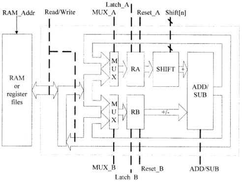
Fig. 6 shows the datapath of the proposed architecture, which includes a 16-bit adder/subtractor and shifter. The adder is a carry-propagation adder to save area cost. The operands and op-erations of the datapath are controlled by a dedicated controller. The input, intermediate results, and final results are stored in the RAM or register files. This datpath is dedicated to the shift-add subexpression. The basic operation of this datapath can be
ex-pressed by , where the “BUS” is the
output of the datapath, the “ ” means right shift by -bit, and the “ ” denotes the add/subtract operation. Therefore, we can store the operands in the registers RA and RB and select the desired one by the MUX from one of the two sources, RAM or BUS. The two registers provide temporary storage to save memory accesses. The shifter in the datapath performs 0–3-bits shift that is suitably designed for the DCT coefficient. In the above subexpression sharing, the maximum number of shifts is six. We split the 6-bit shift operations into two 3-bit shift op-erations, which reduces about 30% of shift hardware and just increases two more computation cycles.
The design of this datapath, contrast to other general pur-pose CPU designs, places the shifter before the adder/subtractor.
Fig. 5. OutputY 0–Y 7 and their common shared terms, where the gray-shaded block is the common shared terms and the block with diagonal pattern is the term without sharing.
Fig. 7 shows the two versions of shifter position designs with an example. From the operation example shown in Fig. 7, we can find that version 1 design is not as efficient as version 2 design, since additional cycles are often required in version 1 design due to improper shifter positions.
The limitation of the datapath is the available RAM band-width and the position of the shifter. In this design, one-port RAM access is assumed for RAM access for simple hardware consideration. To avoid the idle cycles due to the RAM access conflict, we schedule the operation sequences according to their RAM access, which is implemented in the control signal gener-ation. Other solutions, such as multiport RAM access, can also be used to solve this problem. The position of the shifter limits us to do shift and subtraction simultaneously for register RB, since only register RA can perform shift. This limitation can be eliminated by proper operation scheduling.
C. Controller Design and Scheduling
Since the datapath is extremely simple, all the operand se-lections and shared term generation rely on the controller.
Con-Fig. 6. Datapath of the proposed architecture. The broken line means control signals generated from the controller.
Fig. 7. Two versions of shifter position design illustrated with an example.
trollers based on finite-state machines are commonly used in most of the controller designs. However, since no control sig-nals in the proposed design depend on their earlier states, we use a simplified finite-state machine, i.e., a counter-based con-troller, as shown in Fig. 8. Such design is much simpler and more easily adaptive to other transform applications by only changing the combinational circuit part.
The RAM access conflict, which will result in efficiency loss of the design, is eliminated with developed operation scheduling strategies. With all four scheduling techniques, we can complete one 1-D 8-point DCT in 121 cycles that only pays 23 extra cy-cles overhead, as compared with original estimated 98 cycy-cles.
The first strategy is to group operations that have the same
operand and keep one data used continuously. By using this
strategy, we can keep one operand in register RA or RB and read only one register from the RAM. The reloading of the same
Fig. 8. Counter-based controller.
operand is minimized as few as possible. The following is an actual code subsequence in the firmware of this IDCT:
This scheduling example keeps one operand or un-changed, where the boldface is read from RAM. To compute and , the data stays in “RA,” and just
read and to “RB” from RAM. For and
computation, the and stay in “RA” and “RB”, which can save memory read operations to obtain .
The second strategy is to rearrange the operations such that
the output data of current operation is the input of next opera-tions. It will reduce one read cycle of the RAM access. Not all
This example reads one operand from the output bus, where the boldface and denote the data without RAM access. The output data and are fed as input of the next operation to reduce RAM access. When calculating output , the processor uses just one memory read access, and it writes data to RAM at last operation.
The third strategy is to eliminate the memory write access of
the output that will not be used later. If the output will not be
used in later operations, it does not need to be stored in RAM. Rearrange the operations could reduce these memory write op-erations. The following list shows a code example of this case:
This example shows how to reduce the memory write access, where is the output data that does not have to be written to RAM. is used immediately in and calculation, and it will not be used in later operations. Thus, we can avoid writing
into RAM.
Another special case is to swap data in “RA” and “RB” to
solve the constraint of ALU design. If both data are reloaded
from RAM, it will cost two memory read cycles. The following list is a code example that just needs one extra RAM-read cycle to overcome this problem. Original code is
Now use these codes instead
This example swaps the operands data, and . The output data and need both input data and but on dif-ferent operands. We can resolve this by rewriting them into the right one, such that just one memory read cycle instead of two memory read cycles is required.
Fig. 9. Evaluation of different design techniques. TABLE II
HARDWARECOST ANDDELAY OFDCTANDIDCT DESIGNS
IV. HARDWARECOST ANDPERFORMANCE
The number of cycles to compute 1-D 8-point DCT’s is 121, while the number of cycles to compute 1-D 8-point IDCT’s is 119. With the fast direct 2-D DCT algorithm, eight 1-D DCT computations are required, with four butterfly stages. The number of the additions in butterfly stages is 64 3 192 for the first three stages, and 48 for the last stage. So, total
cycle count for the 2-D DCT is .
Similarly, for the 2-D 8 8 IDCT, the number of cycles
required is .
Fig. 9 shows the savings on the number of the additions when we apply different design techniques to compute 2-D 8 8 DCT. This evaluation shows the effectiveness of each technique in the design. The 1-D DCT used in the row–column decom-position is based on the fast algorithm [13] that only requires 11 multiplications and 29 additions for an 8-point DCT with 16-bit precision. We adopt this approach as the relative refer-ence, i.e., the 3104 additions, as 100%. The first significant im-provement comes from the fast direct 2-D DCT algorithm that acounts for 42% reduction. The remaining improvement is from the adder-based DA formulation and subexpression sharing. The RAM-conflict problem in this design adds an extra 6% addition cycles, which can be avoided with larger memory bandwidth support. In the 1208 addition cycles, eight 1-D DCT computa-tions use 968 cycles and the butterfly stage addicomputa-tions use 240 cycles.
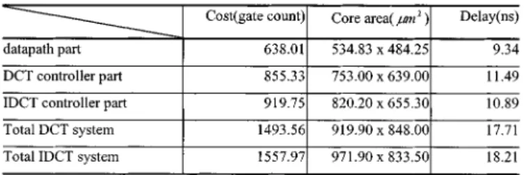
This processor core design for DCT/IDCT with 16-bit word length is synthesized with 0.6- m SPDM CMOS cell library [29]. Table II shows the hardware cost and delay for DCT/IDCT designs. The total gate count of DCT is 1493, which is smaller than one 16 16 multiplier which will consume 2122 gate count for the multiplier with carry–save adder array or 2536 gate count for the multiplier with Wallace tree array. The delay, 18.21 ns,
TABLE III
HARDWAREUTILIZATION FORDCT
TABLE IV
PRECISIONREQUIREMENT ANDSIMULATIONRESULTS OF THEIDCT
is satisfied conservatively with the assumed 33-MHz clock fre-quency.
Table III shows the hardware utilization of each function unit in the 1-D DCT design. The controller is always used in the de-sign and is not listed in the table. The idle cycles in each function unit are due to the available memory bandwidth and the datapath limitation. The overall utilization is quite high for the DCT de-sign. Similar statistics can also be found in the IDCT dede-sign. The precision of the IDCT unit meets the accuracy specifica-tions [30] which are shown in Table IV. Due to DA formulation and proper sharing terms selection, we can use short wordlength to satisfy the precision requirement.
V. APPLICATIONS ANDCOMPARISONS
A. Applications to Various Video Standards
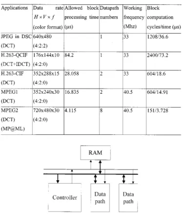
Table V shows the design applications to various video standards. For digital still camera (DSC) that requires low cost while tolerating longer delay, this design can compute all DCT operations within 0.176 s. This delay leaves enough time for other functions such as quantization. Another application is the DCT/IDCT unit in an H.263 codec system. For QCIF size, the proposed design can meet real-time encoding requirements with only one datapath unit.
For larger picture size and higher frame rate, this design can be simply scaled with adding more datapath units or with higher processing clock frequency. Since the datapath part is quite small, even eight datapath units just need 5104 gate counts or 2.07 mm . Fig. 10 shows the scalable design with two datapath units. The bottleneck to the scalable designs is the available memory bandwidth. Larger bus width and multiple port memory can eliminate this problem. Scalable designs also offer the possibility for low-power design. With more datapath
TABLE V
APPLICATIONS TOVARIOUSVIDEOSTANDARDS, WHEREPROCESSINGTIMEIS
ONE82 8 BLOCKCOMPUTATIONTIME
Fig. 10. Scalable designs with two datapath units. TABLE VI
COMPUTATIONTIMECOMPARISONS OFONE82 8 DCTONPROCESSOR
ARCHITECTURES, WHEREMAC DENOTESMULTIPLIER-ACCUMULATE,AND
R.-C. DENOTESROW-COLUMNDECOMPOSITION
units, we can trade the processing power of the parallel units with the lower supply voltages for low power consumption. The datapath numbers of MPEG-2 applications in Table V can be halved at double the clocked rate. The 40.5-MHz clock rate in Table V does not introduce extra cost since the processor delay is 18.21 ns. Higher working frequency can easily be attained by using pipelining or high-speed adders. The tradeoff depends on the target application environment.
B. Comparisons With Other Relevant Approaches
Since the proposed design combines the dedicated ALU data-path and the software-oriented controller, comparisons with pro-cessor-based implementations can show the effectiveness of the proposed design. Table VI lists the computation time compar-isons of one 8 8 DCT executed on our design with that ex-ecuted on DSP processors [17]–[19] or RISC processor with multimedia enhancement [20]. The instruction cycle count in
the table are directly taken from the reference reports or pa-pers. Note that in this paper, we only consider the core com-putation cycles in our design and do not include other system overheads. All the other implementations used fast algorithms in which the direct 2-D fast algorithm requires fewest cycles. Compared with C30 processors [17] that include multipliers, the performance of our proposed design, 1208 cycles, is superior at the similar clock rate. Other design likes that in [18]–[20] use multiple processing units to accelerate the DCT execution. Our proposed design can also attain the same performance by using multiple ALU’s whose cost as shown in Table V is still less than that in [18]–[20]. The proposed design achieves higher perfor-mance by using dedicated datapath unit to accelerate subexpres-sion sharing operation but sacrifices with design flexibility and applicability. In some video applications, incorporating our de-sign as accompany core with conventional DSP processors can provide the advantages of flexible DSP software approach and efficient dedicated hardware accelerator. These advantages are present especially for various inner product computation with either constant coefficients or variable coefficients.
Comparison with dedicated hardware designs is more diffi-cult because of the different approaches used. The proposed de-sign combines software-oriented controller with hardware units, while dedicated hardware designs are pure hardware-oriented approaches. However, Table VII lists the comparisons with ded-icated hardware designs. The data of previous designs are di-rectly taken from the reference papers. All these designs can meet the decoding speed and accuracy of MPEG2 MP@ML (640 480, 30 fps, 4:2:0, 13.82 Mpixels/s). The IDCT core in [7] used digit-serial construction to reduce the overall size. Low-power IDCT in [9], [11] used MAC for computation. The design in [10] was a DCT/IDCT accelerator in a DSP processor based on ROM-based DA. The DCT/IDCT unit in [8] shares the same hardwired multipliers for computations. All five designs are based on row–column decomposition. Compared with these listed designs, the proposed design is very competitive in area cost at the processing rate up to MPEG2 MP@ML decoding. However, for higher throughput rate such as HDTV require-ments, memory bandwidth limits the applicability of the pro-posed design. In such cases, high-speed dedicated hardware de-signs [2]–[6] can provide a more efficient solution.
inner product computations like filters and transforms are easily achieved by applying the design techniques to rewrite the con-troller program. Low-power applications to portable multimedia terminals are possible due to the simple architecture design and low computation cycles.
REFERENCES
[1] K. R. Rao and J. J. Hwang, Techniques and Standards for Image, Video and Audio Coding. Englewood Cliffs, NJ: Prentice-Hall, 1996. [2] P. Pirsch, N. Demassieux, and W. Gehrke, “VLSI architectures for video
compression—A survey,” Proc. IEEE, vol. 83, pp. 220–246, Feb. 1995. [3] M. Kovac and N. Ranganathan, “JAGUAR: A VLSI architecture for JPEG image compression standard,” Proc. IEEE, vol. 83, pp. 247–258, Feb. 1995.
[4] M. T. Sun, T. C. Chen, and A. M. Gottlieh, “VLSI implementation of a
16 2 16 discrete cosine transform,” IEEE Trans. Circuits Syst., vol. 36,
pp. 610–617, Apr. 1989.
[5] A. Madisetti and A. N. Wilson Jr., “A 100 Mhz 2-D8 2 8 DCT/IDCT processor for HDTV applications,” IEEE Trans.Circuits Syst. Video Technol., vol. 5, pp. 158–164, Apr. 1995.
[6] C. Chen, T. Chang, and C. Jen, “The IDCT processor on the adder-based distributed arithmetic,” in Proc. Symp. VLSI Circuits, 1996, pp. 36–37. [7] C.-Y. Hung and P. Landman, “Compact inverse discrete cosine transform circuit for MPEG video decoding,” in Proc. IEEE Workshop Signal Pro-cessing Systems, 1997, pp. 364–373.
[8] Y. Katayama, T. Kitsuki, and Y. Ooi, “A block processing unit in a single-chip MPEG-2 video encoder LSI,” in Proc. IEEE Workshop Signal Processing Systems, 1997, pp. 459–468.
[9] R. Rambaldi, A. Ugazzoni, and R. Guerrieri, “A 35µW 1.1 V gate array
8 2 8 IDCT processor for video-telephony,” Proc. IEEE ICASSP, vol.
5, pp. 2993–2996, 1998.
[10] K. Okamoto et al., “A DSP for DCT-based and wavelet-based video codecs for consumer applications,” IEEE J. Solid-State Circuits, vol. 32, pp. 460–467, Mar. 1997.
[11] T. Xanthopoulos and A. Chandrakasan, “A low-power IDCT macrocell for MPEG2 MP@ML exploiting data distribution properties for minimal activity,” in Proc. Symp. VLSI Circuits, 1998, pp. 38–39.
[12] H. S. Hou, “A fast recursive algorithm for computing the discrete co-sine transform,” IEEE Trans. Acoust., Speech, Signal Processing, vol. ASSP-35, pp. 1455–1461, Oct. 1987.
[13] C. Loeffler, A. Ligtenberg, and G. S. Moschytz, “Practical fast 1-D DCT algorithms with 11 multiplications,” Proc. IEEE ICASSP, vol. 2, pp. 988–991, 1989.
[14] N. I. Cho and S. U. Lee, “Fast algorithm and implementations of 2-D DCT,” IEEE Trans. Circuits Syst., vol. 38, pp. 297–305, Mar. 1991. [15] Y.-P. Lee, T.-H. Chen, L. G. Chen, M. J. Chen, and C. W. Ku, “A
cost-effective architecture for828 two-dimensional DCT/IDCT using direct method,” IEEE Trans. Video Technol., vol. 7, pp. 459–467, June 1997. [16] J. Golston, “Single-chip H.324 videoconferencing,” IEEE Micro., vol.
16, pp. 21–33, Aug. 1996.
[17] W. Houl, “An8 2 8 Discrete Cosine Transform Implementation on the TMS320C25 or TMS320C30,” Texas Instruments, Application Rep. SPRA115, 1997.
[18] TMS320C62x Assembly Benchmarks (1997). [Online]. Available: http://www.ti.com/sc/docs/dsps/products/c6000/62xbench.htm [19] M. Yoshida, H. Ohtomo, and I. Kuroda, “A new generation 16-bit
gen-eral purpose programmable DSP and its video rate application,” in IEEE Workshop on VLSI Signal Processing, 1993, pp. 93–101.
[20] I. Kuroda, “Processor architecture driven algorithm optimization for fast 2-D-DCT,” in IEEE Workshop on VLSI Signal Processing VIII, 1995, pp. 481–490.
[21] D. R. Bull and D. H. Horrocks, “Primitive operator digital filters,” IEE Proc. Circuits Devices Syst., vol. 138, no. 3, pp. 401–412, June 1991. [22] A. G. Dempster and M. D. Macleod, “Constant integer multiplication
using minimum adders,” Proc. IEE Circuits Devices Syst., vol. 141, no. 5, Oct. 1991.
[23] A. G. Dempster and M. D. Macleod, “Use of minimum-adder multiplier blocks in FIR digital filters,” IEEE Trans. Circuits Syst. II, vol. 42, pp. 569–577, Sept. 1995.
[24] R. I. Hartley, “Subexpression sharing in filters using canonic signed digit multipliers,” IEEE Trans. Circuits Syst. II, vol. 43, pp. 677–688, Oct. 1996.
[25] M. Potkonjak, M. Srivastava, and A. P. Chandrakasan, “Multiple con-stant multiplications: Efficient and versatile framework and algorithms for exploring common subexpression elimination,” IEEE Trans. Com-puter-Aided Design, vol. 15, pp. 151–165, Feb. 1996.
[26] A. Peled and B. Liu, “A new hardware realization of digital filters,” IEEE Trans. Acoust., Speech, Signal Processing, vol. ASSP-22, pp. 456–462, Dec. 1974.
[27] S. A. White, “Applications of distributed arithmetic to digital sequence processing: A tutorial review,” IEEE ASSP Mag., vol. 6, pp. 5–19, July 1989.
[28] K. Hwang, Computer Arithmetic: Principles, Architecture, and De-sign. New York: Wiley, 1979.
[29] “Compass 0.6 Micron 5-Volt High Performance Standard Cell Library” (document), Compass, PASSPORT Library, Compass design Automa-tion, San Jose, CA, 1996.
[30] IEEE Standard Specifications for the Implementations of8 2 8 Inverse Discrete Cosine Transform, IEEE Std. 1180-1190.
Tian-Sheuan Chang (S'93) received the B.S. and M.S. degrees in electronics engineering from National Chiao-Tung University, Hsinchu, Taiwan, in 1993 and 1995, where he is currently working toward the Ph.D. degree
His research interest includes VLSI design, digital signal processing, and computer architecture.
Chin-Sheng Kung received the B.S. degree from Na-tional Tsing-Hua University, Taiwan, in 1995, and the M.S. degree from National Chiao-Tung University, Hsinchu, Taiwan, in 1997.
He is currently with Realtek Corporation, Hsinchu, Taiwan. His research interests include VLSI designs, multimedia processing, and digital signal processing.
Chein-Wei Jen (S’78–M’87) received the B.S. degree from National Chiao Tung University, Hsinchu, Taiwan, R.O.C., in 1970, the M.S. degree from Stanford University, Stanford, CA, in 1977, and the Ph.D. degree from National Chiao Tung University, Hsinchu, Taiwan, in 1983.
He is currently a Professor with the Department of Electronics Engineering and the Institute of Electronics, National Chiao Tung University. During 1985–1986, he was a Visiting Researcher with the University of Southern California at Los Angeles. His current research interests include VLSI design, digital signal processing, processor architecture, and design automation. He has held four patents and published over 30 journal papers and 70 conference papers in these areas.
Dr. Jen received the 1990 Best Paper Award from the Engineering Society and the 1994 and 1995 Best Paper Awards from the HD-Media Conference. He was a Program Committee member of ICCD'94 and ICCE 1995–1997, and is a member of Phi Tau Phi.
![Fig. 1. 8 2 8 2-D DCT computation flow of fast direct 2-D DCT algorithms [14], where the cross symbols in the block denote the butterfly additions and the numbers of I/O channels for each stage are all 64.](https://thumb-ap.123doks.com/thumbv2/9libinfo/7893948.155746/2.918.530.757.92.219/computation-direct-algorithms-symbols-butterfly-additions-numbers-channels.webp)