國 立 交 通 大 學
電子工程學系 電子研究所碩士班
碩 士 論 文
利用濕式氧化氮化矽層改善氧化矽/氮化矽/
氧化矽堆疊結構型快閃記憶體之研究
Study on the Improvement of ONO-stacked Flash
Memory by Wet Oxidation of Si
3N
4Layer
研 究 生 :張 子 恒
指導教授 :雷 添 福
堆疊結構型快閃記憶體之研究
Study on the Improvement of ONO-stacked Flash Memory
by Wet Oxidation of Si
3N
4Layer
研 究 生:張子恒 Student:Tzu-Heng Chang
指導教授:雷添福
博士 Advisor:Dr. Tan-Fu Lei
國立交通大學
電子工程學系 電子研究所碩士班
碩士論文
A Thesis
Submitted to Department of Electronics Engineering & Institute of Electronics
College of Electrical Engineering & Computer Engineering
National Chiao Tung University
In Partial Fulfillment of the Requirements
For the Degree of
Master of Science
in
Electronic Engineering
June 2008
Hsinchu, Taiwan, Republic of China
利用濕式氧化氮化矽層改善氧化矽/氮化矽/
氧化矽堆疊結構型快閃記憶體之研究
學生: 張子恒
指導教授: 雷 添 福 博士
國立交通大學
電子工程學系 電子研究所碩士班
摘 要
此論文主要是在研究利用濕式氧化法來製作 SONOS 型非揮發性快閃記憶體 其中的阻障層(blocking layer)。現今大多數的人都使用沉積方式去堆疊阻障層的 氧化層,此論文採用的方式是直接在沉積捕陷電荷層(trapping layer)後,直接將 捕陷電荷層氮化矽 (Si3N4) 材料濕式氧化,來製備阻障層。更進一步的配合捕陷 電荷層的改善,以達成有快速寫入抹除速度、且良好的儲存資料持久性、以及寫 入、清除操作造成的性能退化少的非揮發性快閃記憶體。 首先,我們直接利用濕式氧化去氧化氮化矽去形成阻障層的二氧化矽,可望 利用在氧化時,氧分子可以有比較快的擴散速度,擴散至氮化矽中,進而填補較 淺的捕捉態(trap state),只留下較深處的捕捉態,這樣一來便可增加此記憶體元 件的可靠度。接著,我們為了增加氧化氮化矽的速度,希望在氮化矽上層提供矽原子來氧 化。利用了兩種不同的方式,其一是在氮化矽上層堆疊一層很薄的非晶矽 (amorphous-Si)當作犧牲氧化層(sacrificial layer )。成功的改善了氧化的速度,這 種製程方式會因為沉積很薄的非晶矽,而造成之後的上氧化層會很凹凸不平,可 由原子力顯微鏡(atomic force microscopy, AFM)及穿透式電子顯微鏡(transmission electron microscopy, TEM)來證明。電場在此處的分佈就很不平均,所以此結構的 記憶體元件提供了另一種寫入及抹除的機制,電子改成利用上氧化層來進入捕陷 電荷層,卻亦可維持可接受的可靠度。 最後,另一種方式是利用氮化矽層內嵌奈米矽晶體(Si nano-crystals )來提供 矽原子的成分。在不同高度的氮化矽中放入奈米矽晶體,會因為是否被氧化到而 有不同的特性改善,在放入奈米矽晶體的元件中,若矽晶體在氧化的範圍之內, 便可很明顯的在可靠度方面得到很好的改善。且在氮化矽上放入矽晶體後,在電 荷儲存方式便可更加區域性,使其一個單元儲存兩個位元(two bit per cell),我們 可成功的設計出寫入及取讀條件,並且在儲存兩個位元的時候,依舊可以保持很 好的儲存資料持久性。
Study on the Improvement of ONO-stacked
Flash Memory by Wet Oxidation of Si
3N
4Layer
Student: Tzu-Heng Chang
Advisor: Dr. Tan-Fu Lei
Department of Electronics Engineering &
Institute of Electronics
National Chiao Tung University
ABSTRACT
In this thesis, we mainly study on using wet oxidation to form the blocking layer of the SONOS (poly Si-oxide-nitride-oxide-silicon) type nonvolatile flash memory. Generally, the blocking oxide layers are mostly deposited by furnace. We adopt another way that is the deposited nitride trapping layer was directly oxidized by wet oxidation to form the blocking oxide layer. This nonvolatile memory structure with some changes in trapping layer will have superior characteristics in terms of considerably high speed program/erase, long retention time, and excellent endurance.
First, we present a nonvolatile SONOS type flash memory that was fabricated using wet oxidation to form the oxide layer as the blocking layer from the trapping layer. Oxygen may diffuse faster into the nitride layer, and it can passivate the shallow trap states in nitride. Therefore, there were only the deeper trap states in the trapping layer, and this kind of memory device may have better reliability.
Then, the silicon atoms were provided in the nitride or on top of it for raising the wet oxidation rate. There are two different methods. One of them is that a thin amorphous silicon layer was deposited as the sacrificial layer on the nitride layer. This method successfully improves the oxidation rate. At the same time, the method would form a rough top oxide layer. We can use atomic force microscopy (AFM) and transmission electron microscopy (TEM) to check it. This memory structure would provide another program/erase mechanism, because the electric field was different in the top oxide layer. The electrons injected into the trapping layer through the top oxide layer instead of the bottom oxide layer. This memory still maintains a good reliability.
Finally, the other way is that the silicon source was introduced into the nitride by embedded silicon nano-crystals. Different heights of silicon nano-crystals determine if they are oxidized or not, which results in different improvements. Embedded silicon nano-crystals may improve the reliability or localize the trapping sites. This memory structure can use two bit operation, and still keep good retention.
誌謝
首先在此要向我的指導教授雷添福博士致上最誠摯的敬意與感謝。感謝他 在我加入實驗室這幾年之間,對於學業及研究甚至生活方面的細心指導與照顧。 在這些日子裡,讓我學習到研究的方法及態度,同時學習到許多做人處事的道 理。此外,我亦要感謝趙天生博士在實驗方面給予的教導與幫助,提供了我實驗 的方向,令我獲益良多。 感謝獻德學長帶領我進入半導體的領域,在大學時期一開始做專題時,學長 就給了相當多的指導與照顧。再者,我要感謝俊嘉學長,學長在實驗操作及分析 方面給予了我極大的幫助,總是不厭其煩的幫助學弟,無論自己有多忙多累,卻 不曾拒絕。另外也要感謝已經畢業的伯儀學長、志仰學長、家文學長,在實驗初 期給予的意見及方向,幫助實驗可以更加的順利及完善。而且學長在生活上也帶 領我們參予各種運動,使我們不只在學業上,也在健康上獲得照顧。當然還有很 多已畢業的學長:明山學長、小賢學長、小強學長、建豪學長、紹明學長、小馬 學長,眾多學長的指導與照顧。 也要感謝曾經一起在實驗室研究的學長及同學們:雖然畢業很久但假日出席 率很高的錦石和任逸學長、超好笑但很照顧我的仕傑、很忙但超帥氣交大型男文 呈、可愛的熊貓學長明爵、電動很強的哲綸、籃球超強的久騰、還有伊容學姐、 冠良、文彥、景琳、敬為及春瑀。有大家的陪伴、幫忙與討論,實驗過程雖辛苦 卻不致於乏味。甚至亦提供了實驗室更加團結的話題與氛圍,有大家的幫忙及歡 笑,才能讓我帶著愉快的心情去克服實驗上帶來的挑戰。 最後,謝謝我親愛的家人及女友,還有一群可愛的朋友們,感謝你們在我需 要歡笑及溫暖的時候給我的陪伴及照顧,感謝你們在我心情低落的時候給我的加 油跟鼓勵。謝謝你們陪我度過這不算短的求學生涯。僅此論文獻給我的家人、女 友及所有關心我的朋友。Contents
Abstract (Chinese) ………I
Abstract (English)………III Acknowledge ………V
Contents ………VI
Figure Captions & Table Lists………VIII
Chapter 1 Introduction ………1
1.1 Background……….………….1 1.2 Motivation……….………….5
1.3 Thesis Organization ……….………….6 1.4 Reference……….………….12
Chapter 2 Physical and Electrical Properties of SONOS Memory Using Wet Oxidation………15
2.1 Introduction……….………….15 2.2 Experimental ……….………….16
2.3 Results and discussion……….………….17
2.3.1 Material Analysis of Memory Device
……….………….
17 2.3.2 Characteristics of Fresh Device……….………….182.3.3 Characteristics after P/E Cycling and Disturbance……….………….18 2.4 Summary……….………….19
2.5 Reference……….………….33
Chapter 3 Physical and Electrical Properties of SONOS Memory Using Wet Oxidation with Sacrificial Silicon Layer………35
3.1 Introduction……….………….35 3.2 Experimental……….………….36
3.3 Results and Discussion……….………….37
3.3.1 Analysis the Structure of Top Oxide Layer……….………….37
3.3.2 Operation of SONOS Memory with Textured Oxide……….………….38 3.3.3 Characteristics of P/E Cycling……….………….39
3.4 Summary……….………….40 3.5 Reference……….………….51
Chapter 4 Characteristics of SONOS Memory Using Wet Oxidation with Embedded Silicon Nano-crystals in Nitride Layer………53
4.1 Introduction……….………….53 4.2 Experimental……….………….54
4.3 Results and Discussion……….………….55
4.3.1 Material Analysis of Memory Device……….………….55 4.3.2 Characteristics of Fresh Device……….………….55
4.3.3 Characteristics after P/E Cycling and Disturbance……….………….56 4.3.4 Two-bit operation and migration of charges storage……….………….58 4.4 Summary ……….………….59
4.5 Reference……….………….77
Figure Captions
Chapter 1
Fig. 1-1 The semiconductor memory tree. ……….………….7
Fig. 1-2 Schematic of a basic ETOX Flash memory device. ……….………….7 Fig. 1-3 Electron flow and hole flow during programming or erasing. ……….……8 Fig. 1-4 The basic current-voltage characteristic. ……….………….8
Fig. 1-5 (a) The cross-section of a SONOS structure. ……….………….9
Fig. 1-5 (b) The band diagram of nitride- based SONOS memory. ……….………….9 Fig. 1-6 (a) The memory with continuous traps and charge leakage mechanism. …10 Fig. 1-6 (b) The memory with discrete traps and charge leakage mechanism……..10 Fig. 1-7 (a) Vertical migration in the trapping layer. ……….………….11
Fig. 1-7 (b) Lateral migration in the trapping layer. ……….………….11
Chapter 2
Fig. 2-1 The process flow and the cross-section of the flash memory. ……….……23 Fig. 2-2 The C-V characteristics of ONO gate stacks. ……….………….25
Fig. 2-3 The TEM image of proposed ONO gate stack. ……….………….27
Fig. 2-4 Program speed curves of SONOS-type memory using wet oxidation. ……28 Fig. 2-5 Erase speed curves of SONOS-type memory using wet oxidation. ……….29 Fig. 2-6 The endurance characteristics of the memory cell using wet oxidation after
10k P/E cycling. ……….………….30
Fig. 2-7 The retention characteristics of the memory cell using wet oxidation……31 Fig. 2-8 Gate disturbance characteristics of the memory devices. A threshold voltage
shift of only 0.21 V occurred after stressing at Vg = 6 V and Vs = Vd = Vsub = 0 V for 1000 s. ……….………….32
Chapter 3
Fig. 3-1. The special parts of process flow and the cross-section of the flash memory. ……….………….42
Fig. 3-2 The C-V characteristics of ONO gate stacks. ……….………….43
Fig. 3-3 The AFM of nitride layer with 50A-thick a-Si after WET300 recipe oxidation. ……….………….44
Fig. 3-4 The AFM of nitride layer without a-Si after 900oC 120 mins oxidation……45 Fig. 3-5 The TEM image of proposed ONO gate stack. The image clearly shows the
textured structure of top oxide layer. ……….………….46
Fig. 3-6 The program speed curves of SONOS-type flash memory with textured top oxide. ……….………….47
Fig. 3-7 The erase speed curves of SONOS-type flash memory with textured top oxide. ……….………….48
Fig. 3-8 The endurance characteristics of the memory cell with textured top oxide...49 Fig. 3-9 The retention characteristics of the memory cell with textured top oxide….50
Chapter 4
Fig. 4-1 Cross section and process flow of the SONOS-type flash memory device. ..60 Fig. 4-2 The gas flow of silicon nano-crystal deposited in nitride layer. ……….…...61 Fig. 4-3 The TEM image of proposed ONO gate stack. ……….………….63
Fig. 4-4 The program and erase speed curves of the memory which was oxidized in 180 minutes and had silicon nano-crystals in the nitride layer at 60A to the bottom. ……….………….64
Fig. 4-5 The program and erase speed curves of the memory which was oxidized in 180 minutes and had silicon nano-crystals in the nitride layer at 120A to the bottom. ……….………….65
Fig. 4-6 The endurance characteristics of the memory cell which was oxidized in 180 minutes and had silicon nano-crystals in the nitride layer at 60A to the bottom. ……….………….66
Fig. 4-7 The endurance characteristics of the memory cell which was oxidized in 180 minutes and had silicon nano-crystals in the nitride layer at 120A to the bottom. ……….………….67
Fig. 4-8 The retention characteristics of the memory cell which was oxidized in 180 minutes and had silicon nano-crystals in the nitride layer at 60A to the bottom. ……….………….68
Fig. 4-9 The retention characteristics of the memory cell which was oxidized in 180 minutes and had silicon nano-crystals in the nitride layer at 120A to the bottom. ……….………….69
Fig. 4-10 Gate disturbance characteristics of the memory cell which was oxidized in 180 minutes and had silicon nano-crystals in the nitride layer at 60A to the bottom. ……….………….70
Fig. 4-11 Gate disturbance characteristics of the memory cell which was oxidized in 180 minutes and had silicon nano-crystals in the nitride layer at at 120A to the bottom. ……….………….71
Fig. 4-12 Ids–Vgs Curves of the two-bit memory in a cell; forward read and reverse read for programmed bit-D and programmed bit-S. ……….………….72 Fig. 4-13 The two-bit retention characteristic of the silicon nano-crystals memory...74 Fig. 4-14 The two-bit retention characteristic of the SONOS-type memory………75 Fig. 4-15 The bit-S retention characteristic of the memories measured at 75oC.
Table Lists
Chapter 2
Table 2-1 The estimated thickness of top oxide layers. ……….………….26
Chapter 4
Table 4-1 The split condition of our experiment device with different height of the silicon nano-crystals. ……….………….62
Table 4-2 Operation principles and bias conditions utilized during the operation of the silicon nano-crystals Flash memory cell. ……….………….73
Chapter 1
Introduction
1.1 Background
Now, the complementary metal-oxide-semiconductor (CMOS) memory technologies are widely used in mobile capabilities, computers, global positioning systems and some other electronic consumer products.
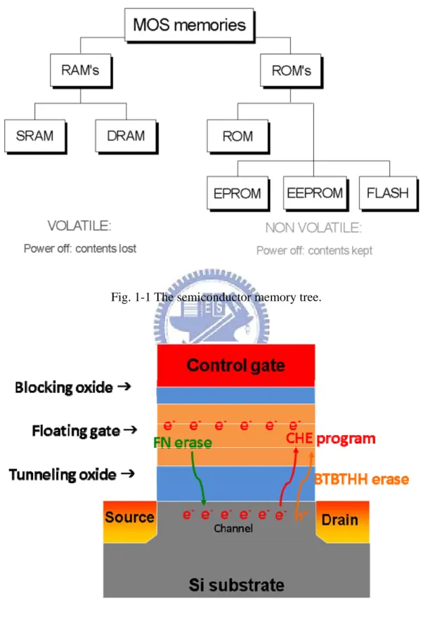
As we know, memories can be divided into two main categories depending on whether the storage data can be affected by the power supply. One is volatile memory, and the other is non-volatile memory. As its name suggests, volatile memories will lose the storage data if the power supply is turned off. Non-volatile memories can keep the stored information when the device is turned off, and at the same time, offer low power and high storage density solutions to generic needs of data storage [1.1]. The semiconductor memory tree is shown in Figure 1-1.
In the memory family, Flash has the most explosive growth and owns the most advantages. Flash offers the best compromise between these two parameters, flexibility and cost. Flexibility indicates the possibility to be programmed and erased many times on the system with minimum granularity (whole chip, page, byte, bit); cost relates to process complexity and, in particular, silicon occupancy, i.e., density or, in simpler words, cell size. Flash has the smallest cell size which is one transistor cell with a very good flexibility. Flash can be electrically written on field for more than 100k times with byte programming and sectors erasing [1.2].
The most well-known commercial Flash memory is the Intel ETOX (EPROM Tunnel Oxide) structure (Figure 1-2) [1.3]. The basic device is a Metal-Oxide-Semiconductor-Field-Effect-Transistor (MOSFET) with a gate stack
which has two gates, control gate and floating gate, embedded in a dielectric material such as silicon dioxide (SiO2). This structure was first invented by D. Kahug and S. M. Sze at Bell Labs in 1967 [1.4]. The memory uses the isolated floating gate to store data. Figure 1-2 shows the mechanism of programming and erasing state and its location. Figure 1-3 shows the band diagram of programming and erasing operations [1.5]. When the electrons are programmed into the floating gate by Channel-Hot-Electron (CHE) programming, the ETOX goes to the “programming” state. In this state, the threshold voltage (VTH) would increase in the case of an nMOSFET. On the other hand, Fowler-Nordheim (FN) tunneling or band to band hot hole (BTBHH) injection injects the electrons from floating gate. The VTH would decrease back to the initial voltage in an ideal case. The voltage difference between the programming state and erasing state is called the memory window. Figure 1-4 shows the basic current-voltage characteristic. After we plot the current-voltage curve, we can fix a constant voltage between the VTH of programming state and erasing state to sense memory state.
The ETOX device uses floating gate to achieve high densities, good program/erase speed, and good reliability for Flash memory applications. Nevertheless, the ETOX cell has several main drawbacks. First, for the superior retention and endurance characteristics, the memory devices requires thicker tunnel oxide (8~10nm). The thick tunnel oxide causes higher operation voltage, slower program/erase speed, and poor scalability issues. Second, the poly-silicon floating gate is a continuous material. The charge stored in floating gate would easily be leaked through the tunnel oxide during P/E cycles. If there is only one leakage defeat, all charges in the floating gate would leak away [1.6]. Third, scaling the ETOX cell below 0.1um feature size is difficult. The main problems are related to the high
stressing and the leaky scaled-down oxide barrier during P/E cycles.
Because of the drawbacks mentioned above, a new memory structure with discrete traps as charge storage elements is used to overcome those drawbacks. The SONOS-type (poly-Si-oxide-nitride-oxide-silicon) structure memories [1.7-1.8] and nano-crystals memories are the better candidates in the Flash memory application [1.9].
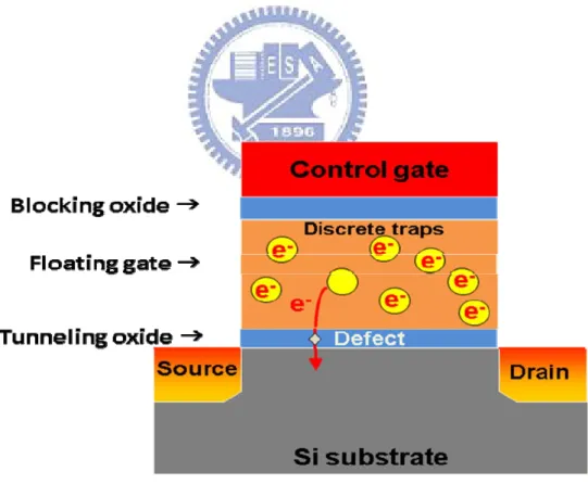
The SONOS-type flash memories have recently attracted much attention for their application in the next-generation nonvolatile memories [1.10]. Figure 1-5(a) illustrates the cross-section of a SONOS structure. Figure 1-5(b) is the band diagram of a nitride- based SONOS memory [1.11]. When the control gate is applied with a positive bias, the electrons may tunnel through the tunneling oxide from the channel and be trapped in the nitride layer. Alternatively, when a negative bias is applied on the control gate, the negative charge in the nitride layer would inject into the channel by directly tunneling. The electrons in the nitride layer would be blocked by the blocking oxide or tunneling oxide because of the shallow trap level in the nitride layer [1.12]. This memory structure with a nitride trapping layer can provide a good retention time, because of the discrete traps of the nitride layer. Unlike the floating gate, the nitride trapping layer does not leak all charges during P/E cycles. Figure 1-6 illustrates the difference between continuous traps and discrete traps.
SONOS-type memory devices have several advantages including fast programming, low power operation, high-density integration, and good endurance characteristics [1.13-1.16]. However, to avoid the degradation of retention characteristics by tunneling leakage through ultra thin tunnel oxide, the optimization of the tunnel oxide thickness is necessary.[1.17] The optimization of the blocking layer is also necessary to avoid electron tunneling through the blocking oxide during
the erase condition, which in turn causes an under erased problem [1.18-1.20].
The deposited silicon dioxide layer, TEOS (tetraethyl orthosilicate), is commonly used as blocking layer. In this thesis, we want to use wet oxidation to form silicon dioxide from nitride. The oxidized nitride can provide a better quality for blocking electron injection from trapping layer to the gate. During wet oxidation, the oxygen diffuses into the nitride layer and passivates the shallow traps in the nitride [1.21]. The retention time should be improved when there are only deep traps in the nitride. Using the oxidized nitride layer as blocking oxide can increase the retention time, but it takes a long time to oxidize the nitride into oxide [1.22-1.23]. To solve this problem, we need to supply the silicon source during wet oxidation. Method one is that an amorphous silicon layer is deposited on the nitride layer as a sacrificial layer. During oxidation, this sacrificial layer can transfer into silicon dioxide easily and quickly. At the same time, the oxygen can also diffuse into the nitride layer for passivating the shallow traps. It takes another mechanism to program and erase operation [1.24]. This structure would be discussed in chapter 3.
In the next chapter, we put silicon nano-crystals into the nitride layer. The nitride layer with nano-crystals is used as the trapping layer which provides a high quality in terms of retention and program/erase speed. Now, we want to use silicon nano-crystals to offer silicon atoms for accelerating the wet oxidation. In order to assure the silicon nano-crystals are not be oxidized, we used the same furnace as the furnace which is used for depositing nitride layer. This way uses the horizontal furnace system to change the gas flow ratio between SiH2Cl2 and NH3. When there are both SiH2Cl2 and NH3 in the furnace, the nitride layer is deposited. When we only turn off the flow of NH3 gas, the silicon nano-crystals are deposited above the nitride layer. Finally, we turn the flow of NH3 gas back on, and the nitride layer is deposited
to cap the silicon nano-crystals. Using silicon nano-crystals seems to improve the retention time and program/erase speed. The mechanism of lateral migration and vertical migration is illustrated in Figure 1-7. Lateral migration can be reduced effectively by the introduction of nano-crystals. The nano-crystals in the nitride layer may also improve the retention of two bit per cell operation by reducing the lateral migration [1.25]. Nitride with silicon nano-crystals is a better material for wet oxidation.
1.2 Motivation
In this thesis, we designed a high performance nonvolatile memory with an oxidized nitride layer as blocking oxide layer. Part of the trapping layer, nitride, was transformed into oxide as blocking layer by wet oxidation in the SONOS structure. Compared to a deposited blocking oxide layer, an oxidized blocking oxide layer has more compact structure which improves reliability. This nonvolatile memory structure would have superior characteristics in terms of long retention time.
There are many trap states in the trapping nitride layer, and some of these are shallow trap states which trapped charges in could easily flow away. This mechanism would decrease the retention time or the reliability. It is expected that oxygen would have a higher diffusivity in wet oxidation than dry oxidation. When the nitride layer was oxidized by wet oxidation, the oxygen diffuses rapidly into the nitride layer and passivates the shallow trap states. Only deep trap states are remained in the trapping layer, and this nonvolatile memory structure should have a good reliability in retention time.
When the nitride layer was oxidized into oxide layer the amount of silicon atoms in the nitride layer plays an important role in the oxidation time and the quality of
oxide. In the thesis, we used two methods to provide the silicon source. First, a thin amorphous silicon layer was deposited on top of the nitride layer. Then wet oxidation was used to form the top oxide layer. This process would produce a different structure in the top oxide layer which provides a different program/erase mechanism. A higher program/erase speed can be used, but the retention time would be decreased.
The other silicon source is the embedded silicon nano-crystals in the nitride layer. Different heights of the nano-crystal in nitride show different qualities. Embedded silicon nano-crystals could improve the retention time and the characteristic of two-bit operation.
1.3 Thesis Organization
We will propose the SONOS type memory devices with different ways of forming blocking layers and trapping layers by wet oxidation. In Chapter 1, we introduced the background of the flash memory and SONOS-type memory.
Wet oxidation of deposited nitride serving as the blocking layer would be shown in chapter 2. In this chapter, we measure the electrical properties and discuss its performance.
In chapter 3, we will add a sacrificial Si layer on top of the trapping layer for faster oxidation. This method gives another structure in the top oxide layer, and also changes the program/erase mechanism of the memory device.
In chapter 4, the embedded silicon nano-crystals in the trapping layer play an important role for the memory characteristics. We will split two conditions with the height of silicon nano-crystal in trapping layer. Different conditions show different improvement in retention or two-bit-per-cell characteristics.
Fig. 1-1 The semiconductor memory tree.
Fig. 1-3 Electron flow and hole flow during programming or erasing [1.5].
Fig. 1-5(a) The cross-section of a SONOS structure.
SiO
2SiO
2n
+poly- Si
SiN
xp-sub
1.05eV
3.1eV
3.1eV
1.1eV
5.1eV
1.1eV
4.6eV
4.6eV
2.65eV
Fig. 1-5(b) The band diagram of a nitride- based SONOS memory.Fig. 1-6(a) The memory with continuous traps and charge leakage mechanism.
Fig. 1-7(a) Vertical migration in the trapping layer.
1.4 Reference
[1.1] R. Bez, E. Camerlenghi, A. Modelli, and A. Visconti, “Introduction to Flash Memory”, Proc. of the IEEE, 91, 489, 2003.
[1.2] P. Pavan, R. Bez, P. Olivo, and E. Zanoni,”Flash Memory Cells—An Overview”, Proc. of the IEEE, 85, 1248, 1997.
[1.3] Stephen Keeney, “A 130nm Generation High Density ETOXTM Flash Memory Technology”, IEDM Tech. Dig., p.41-44, 2001.
[1.4] D. Kahug and S. M. Sze, Bell Syst. Tech. J. 46, 1288, 1967.
[1.5] VY Aaron, JP Leburton, “Flash memory: towards single-electronics”, Potentials, IEEE, 2002.
[1.6] Barbara De Salvo, Gerard Ghibaudo, Georges Pananakakis, Gilles Reimbold, Francois Mondond, Bernard Guillaumot, and Philippe Candelier, “Experimental and theoretical investigation of nonvolatile memory data-retention,” IEEE Trans. Electron Devices, vol. 46, no. 7, pp. 1518-1524, Jul., 1999.
[1.7] Boaz Eitan, Paolo Pavan, Ilan Bloom, Efraim Aloni, Aviv Frommer, and David Finzi, “NROM: A Novel Localized Trapping, 2-Bit Nonvolatile Memory Cell,” IEEE Electron Device Lett., vol. 21, no. 11, pp. 543-545, Nov. 2000.
[1.8] Marvin H. White, Dennis A. Adams, and Jiankang Bu, “Effects of Two-step High Temperature Deuterium Anneals on SONOS Nonvolatile Memory Devices”, IEEE Electron Device Letters, vol.22, No1, Jan. 2001.
[1.9] S. Tiwari, F. Rana, K. Chan, H. Hanafi, W. Chan, and D. Buchanan, “Volatile and Non-Volat ile Memories in Silicon with Nano-Crystal Storage”, IEDM Tech. Dig. P.521-524, 1998.
[1.10] M. H. White, D. A. Adams, and J. Bu,” On the go with SONOS” IEEE Circuits Devices Mag., 2000.
[1.11]. Y.-N. Tan, W.-K. Chim, B. J. Cho, and W.-K. Choi,” Over-Erase Phenomenon in SONOS-Type Flash Memory and its Minimization Using a Hafnium Oxide Charge Storage Layer”, IEEE Trans. Electron Devices, 51, 1143, 2004.
[1.12] T. Sugizaki, M. Kobayashi, M. Ishidao, H. Minakata, M. Yamaguchi, Y. Tamura, Y. Sugiyama, T. Nakanishi, and H. Tanaka, “Novel multi-bit SONOS type flash memory using a high-k charge trapping layer,” in Proc. VLSI Symp. Technology Dig. Technical Papers, 2003.
[1.13] Sanghun Jeonz and Chungwoo Kim, “The Effect of Fixed Oxide Charge in Al2O3 Blocking Dielectric on Memory Properties of Charge Trap Flash Memory Devices” Electrochemical and Solid-State Letters, 2006.
[1.14] Peiqi Xuan, Min She, Bruce Harteneck, Alex Liddle, Jeffrey Bokor, and Tsu-Jae King, “FinFET SONOS Flash memory for embedded applications,” in IEDM Tech. Dig., 2003, pp. 609-613.
[1.15] M. K. Cho and D. M. Kim,”High performance SONOS memory cells free of drain turn-on and over-erase: compatibility issue with current flash technology” IEEE Electron Device Lett., 2000.
[1.16] C. W. Oh, S. D. Suk, Y. K. Lee, S. K. Sung, J.-D. Choe, S.-Y. Lee, D. U. Choi, K. H. Yeo, M. S. Kim, S.-M. Kim, M. Li, S. H. Kim, E.-J. Yoon, D.-W. Kim, D. Park, K. Kim, and B.-I. Ryu, “Damascene gate FinFET SONOS memory implemented on bulk silicon wafer” Tech. Dig. Electron Devices Meet., 2004. [1.17] M. L. French, CY Chen, H Sathianathan, MH White, “Design and scaling of a
SONOS multidielectric device for nonvolatile memory applications” IEEE Trans. Compon., Packag. Manuf. Technol., 1994.
[1.18] Sangmoo Choi, Myungjun Cho, Jung Woo Kim and Hyunsang Hwang, “Improved metal–oxide–nitride–oxide–silicon-type flash device with high- k
dielectrics for blocking layer” JOURNAL OF APPLIED PHYSICS, vol. 94, pp. 5409-5410, 2003.
[1.19] J. Bu and M. H. White, “Design considerations in scaled SONOS nonvolatile memory devices” Solid-State Electron. 2001.
[1.20] F. R. Libsch, MH White, “Charge transport and storage of low programming voltage SONOS/MONOS memory devices.” Solid-State Electron. 1990.
[1.21] Sang-Eun Lee, Byungcheul Kimb, Joo-Yeon Kimc Ho-Myoung ,and Kwang-Yell Seo, “Quantitative analysis of chemical compositions in ultra-thin oxide–nitride–oxide stacked films having wet oxidized blocking layer” Elsevier B.V. Thin Solid Films, 2007.
[1.22] Sang-Eun Lee, Byungcheul Kimb, Joo-Yeon Kimc Ho-Myoung ,and Kwang-Yell Seo, “Quantitative analysis of chemical compositions in ultra-thin oxide–nitride–oxide stacked films having wet oxidized blocking layer” Elsevier B.V. Thin Solid Films, 2007.
[1.23] E Suzuki, Y Hayashi, K Ishii, T Tsuchiya, “Traps created at the interface between the nitride and the oxide on the nitride by thermal oxidation” Appl. Phys. Lett., 1983.
[1.24] Chih-Chieh Yeh,Tahui Wang, Wen-Jer Tsai, Tao-Cheng Lu, Ming-Shiang Chen, Yi-Ying Liao,Wenchi Ting, Yen-HuiJoseph Ku,and Chih-Yuan Lu, “A Novel PHINES Flash Memory Cell with Low Power Program/Erase, Small Pitch ,Two-Bits-Per-Cell For Data Storage Applications” IEEE TRANS. ON ELECTRON DEVICES, VOL.52, NO.4, 2005.
[1.25] Yao-Wen Chang; Tao-Cheng Lu; Sam Pan; Chih-Yuan Lu, “Modeling for the 2nd-bit effect of a nitride-based trapping storage flash EEPROM cell under two-bit operation”, IEEE Electron Device Lett., vol. 25, pp. 95-97, Feb. 2004.
Chapter 2
Physical and Electrical Properties of
SONOS Memory Using Wet Oxidation
2.1 Introduction
As we know, the SONOS-type (poly-Si-oxide-nitride-oxide-silicon) flash memories have recently attracted much attention for their application in the next-generation nonvolatile memories [2.1].
SONOS-type memory devices have several advantages including fast programming speed, low power operation, high-density integration, and good endurance characteristics [2.2-2.5]. However, to avoid the degradation of retention characteristics caused by electrons tunneling through the ultra thin tunneling oxide, optimization of the tunnel oxide thickness is necessary.[2.6] The optimization of the blocking layer is also necessary to avoid electrons tunneling through the blocking oxide during the erase condition, which in turn causes an under-erase problem [2.7-2.9].
The deposited silicon dioxide layer, TEOS (tetraethyl orthosilicate), is commonly used as the blocking layer. The gate injection issue and short retention time would occur when using TEOS oxide as the blocking layer. The reason is that the quality of the deposited blocking layer is not good enough to prevent electron injection from gate. In this chapter, the nitride layer used as the trapping layer would be oxidized to form the blocking layer. The oxidation method offers several significant advantages. First, the quality of a thermal top oxide is higher in comparison to that of a deposited oxide. Second, an oxy-nitride transition layer with increased charge storage ability forms between the top oxide and the nitride layer [2.10-2.11]. Third, it suggests that
oxygen which diffused into the nitride passivates the shallow traps in the nitride near the blocking oxide when wet oxidation was taken place. Therefore, charge carriers injected into the nitride are stored in deep traps of the nitride, and memory characteristics of SONOS devices are improved [2.12].
In this chapter, we fabricate the SONOS-type memory using wet oxidized nitride as blocking layer. We analyze the quality of the wet oxidized blocking layer by examining its program/erase speed, charge retention time, endurance and XTEM images.
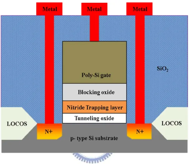
2.2 Experimental
The process flow of the proposed SONOS flash memory is shown in Figure 2-1. The fabrication of a wet oxidized nitride SONOS-type memory started with a LOCOS isolation process on a p-type (100) 150-mm silicon substrate. First, a 3 nm thick tunnel oxide was thermally grown at 1000oC in a vertical furnace system. After that, the trapping layer, nitride layer, was deposited by a horizontal furnace. The thickness of the trapping layer was about 15 nm. The main step of this structure was the fabrication of the blocking oxide. The top part of the nitride was oxidized by wet oxidation for 120 minutes or 180 minutes at 900oC. After the ONO gate stack was formed, the 200nm-thick poly gate electrode was deposited by a horizontal furnace. Then, the gate electrode was patterned. For NMOSFET, the source/drain and gate were doped by self-aligned P ion implantation at the dosage and energy of 5×10¹⁵ ions/cm2 and 20 KeV. The substrate contact was patterned and the sub-contact was implanted with BF2 at the dosage and energy of 5×10¹⁵ ions/cm2 and 40 KeV. After these implantations, those dopants were activated under rapid thermal annealing at 1050OC for 5 seconds. The rest of the subsequent standard CMOS procedures were completed to fabricate the memory devices.
2.3 Results and Discussion
2.3.1 Material Analysis of Memory Device
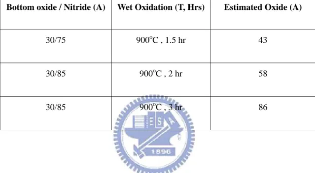
We fabricated SONOS-type capacitors to check the oxidation rate in the first place. Figure 2-2 illustrates the capacitance versus the applied voltage curves under three different conditions: wet oxidation for 90 minutes, 120 minutes and 180 minutes. The oxidized nitride layer was transformed into the top oxide layer as blocking layer. As the C-V curves show, there is hysteresis even in the 180 minutes case. It indicates the nitride layer may not be transformed into oxide totally. We used some reference to estimate for the thickness of the top oxide which was transformed from nitride [2.12-2.13]. In our recipe for depositing nitride, the SiH2Cl2 was in 30 sccms and NH3 was in 130 sccms. The ratio of nitride to silicon dioxide is 1:1.69. We set the transformation in the linear region so that it is controlled by surface diffusion and oxidation. Table 2-1 shows the estimated thickness of the top oxide. As the table shows, the conditions of wet oxidation for 120 and 180 minutes are suitable thicknesses for the top oxide as the blocking layer.
Figure 2-3 illustrates the cross section of the ONO gate stack by transmission electron microscopy (TEM). This sample was oxidized for 180 minutes. As the image shown, the thickness of the blocking oxide is about 5 nm. There is quite a difference between the real thickness and the estimated one. This indicates that the oxidation rate was not linear for this thickness or we overestimated the rate at first. It took three hours oxidizing the nitride, and there was only a 5nm-thick oxide. The oxidation rate should be raised for better applications.
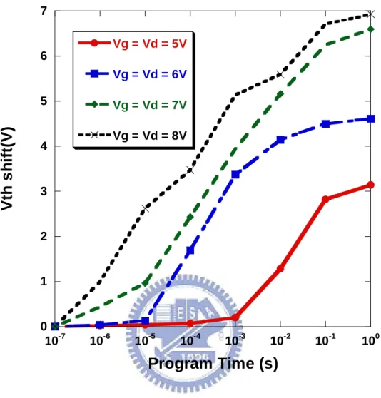
2.3.2 Characteristics of Fresh Device
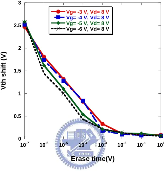
Figure 2-4 illustrates the program speed curve of the memory using 180-munutes wet oxidation. We use channel hot electron injection (CHEI) mechanism to program the memory cell. Here, we show four different stress conditions: Vg=Vd=5V, Vg=Vd=6V, Vg=Vd=7V and Vg=Vd=8V. When the programming gate voltage becomes more positive, more hot electrons are generated in the channel. The generated electrons would be trapped in the nitride layer and causing Vt to shift positively. As the figure shows, the condition Vg=Vd=6V, 1msec causes Vt to shift over 3V. The condition Vg=Vd=8V, 1msec causes Vt to shift even over 5V. Figure 2-5 illustrates the erase speed curve of the memory using 180-minutes wet oxidation in. We use band to band hot hole (BTBHH) mechanism to erase. There are four conditions: Vg/Vd = -3V/8V, -4V/8V, -5V/8V and -6V/8V. We can see that Vt shift > 2V in 1msec under all stress conditions. There is no electron back tunneling and over-erase during erasing. As the figure shows, the final erase state would not go back to the initial state. This may affect the endurance characteristics and we wili discuss it later.
2.3.3 Characteristics after P/E Cycling and Disturbance
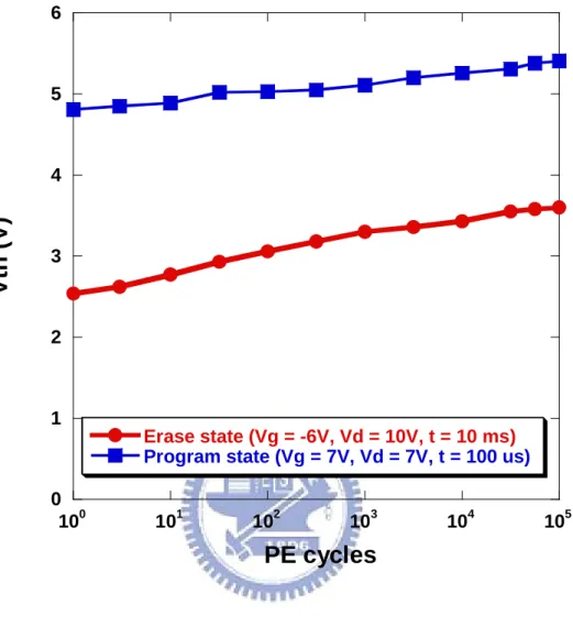
Figure 2-6 shows the endurance characteristics of the memory cell. The programming and erase conditions were Vg = 7V, Vd = 7V for 100 usec and Vg = -6V, Vd = 10V for 10ms, respectively. Remarkably, Vt in the program state increases about 0.5V and increases about 1V in the erase states after 105 P/E cycles. The spatial distributions for electrons and holes are localized during the channel hot-electron injection and band-to-band hot-hole injection for the programming and erasing
operation of our SONOS memory. If the electron distribution does not completely match that of the hole, a few electrons are left behind in the trapping layer after each P/E cycle [2.14]. This so-called “hard-to-erase” phenomenon cannot be eliminated readily when using band-to-band hot-hole erasing. Up to 105 P/E cycles, there is still a memory window of 2V, which is an acceptable endurance for the memory cell.
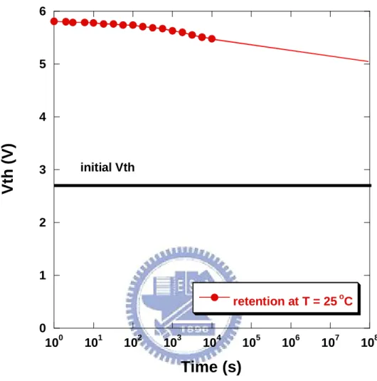
Figure 2-7 shows the data retention characteristic of SONOS memory measured at 25oC. Relative to the fresh device, the device operated at room temperature retained its good retention time (up to 105 s) for 10% charge loss. We ascribe this result to the effect of shallow trap states which were passivated by oxygen atoms during wet oxidation.
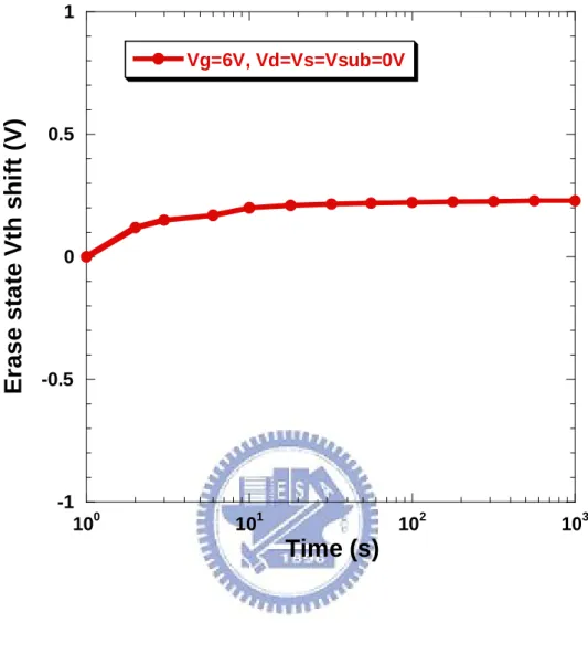
Figure 2-8 shows the gate disturbance characteristics in the erase state. Gate disturbance may occur during programming one of the cells sharing a common word-line
.
We observed a threshold voltage shift of only 0.21 V, i.e., negligible disturbance, under the following condition: Vg = 6 V, Vs = Vd = Vsub = 0 V, and 1000s stress. When the gate electrode was applied with a voltage, the voltage drop at the tunneling layer was too little to cause a noticeable direct tunnel current. The blocking layer also provides a good barrier for avoiding gate injection.2.4 Summary
In this chapter, we successfully used wet oxidation to form the blocking oxide layer of the ONO gate stack from the nitride layer. The devices show high program/erase speed and good disturbance characteristics. The cells also show an acceptable endurance and long retention time after 10K P/E cycles. We can raise the oxidation rate to fabricate a device with a better performance in chapter 4.
Table 2-1 The estimated thickness of top oxide layers.
Bottom oxide / Nitride (A) Wet Oxidation (T, Hrs) Estimated Oxide (A)
30/75 900oC , 1.5 hr 43
30/85 900oC , 2 hr 58
0 1 2 3 4 5 6 7 10-7 10-6 10-5 10-4 10-3 10-2 10-1 100 Vg = Vd = 5V Vg = Vd = 6V Vg = Vd = 7V Vg = Vd = 8V
Vth s
h
ift(V)
Program Time (s)
0 0.5 1 1.5 2 2.5 3 10-7 10-6 10-5 10-4 10-3 10-2 10-1 100 Vg= -3 V, Vd= 8 V Vg= -4 V, Vd= 8 V Vg= -5 V, Vd= 8 V Vg= -6 V, Vd= 8 V
Vth s
h
ift (V)
Erase time(V)
Fig. 2-5 Erase speed curves of SONOS-type memory using wet oxidation.
0 1 2 3 4 5 6 100 101 102 103 104 105 Erase state (Vg = -6V, Vd = 10V, t = 10 ms)
Program state (Vg = 7V, Vd = 7V, t = 100 us)
Vth (V)
PE cycles
Fig. 2-6 The endurance characteristics of the memory cell using wet oxidation after 10k P/E cycling.
0 1 2 3 4 5 6 100 101 102 103 104 105 106 107 108 retention at T = 25oC
Vth (V)
Time (s)
initial Vth-1 -0.5 0 0.5 1 100 101 102 103 Vg=6V, Vd=Vs=Vsub=0V
E
ras
e
s
ta
te
V
th
sh
if
t
(V
)
Time (s)
Fig. 2-8 Gate disturbance characteristics of the memory devices. A threshold voltage shift of only 0.21 V occurred after stressing at Vg = 6 V and Vs = Vd = Vsub = 0 V for
2.5 Reference
[2.1] M. H. White, D. A. Adams, and J. Bu,” On the go with SONOS” IEEE Circuits Devices Mag., 2000
[2.2] Sanghun Jeonz and Chungwoo Kim, “The Effect of Fixed Oxide Charge in Al2O3 Blocking Dielectric on Memory Properties of Charge Trap Flash Memory Devices” Electrochemical and Solid-State Letters, 2006
[2.3] Peiqi Xuan, Min She, Bruce Harteneck, Alex Liddle, Jeffrey Bokor, and Tsu-Jae King, “FinFET SONOS Flash memory for embedded applications,” in IEDM Tech. Dig., 2003, pp. 609-613.
[2.4] M. K. Cho and D. M. Kim,”High performance SONOS memory cells free of drain turn-on and over-erase: compatibility issue with current flash technology” IEEE Electron Device Lett., 2000.
[2.5] C. W. Oh, S. D. Suk, Y. K. Lee, S. K. Sung, J.-D. Choe, S.-Y. Lee, D. U. Choi, K. H. Yeo, M. S. Kim, S.-M. Kim, M. Li, S. H. Kim, E.-J. Yoon, D.-W. Kim, D. Park, K. Kim, and B.-I. Ryu, “Damascene gate FinFET SONOS memory implemented on bulk silicon wafer” Tech. Dig. - Int. Electron Devices Meet., 2004,
[2.6] M. L. French, CY Chen, H Sathianathan, MH White, “Design and scaling of a SONOS multidielectric device for nonvolatile memory applications” IEEE Trans. Compon., Packag. Manuf. Technol., 1994
[2.7] Sangmoo Choi, Myungjun Cho, Jung Woo Kim and Hyunsang Hwang, “Improved metal–oxide–nitride–oxide–silicon-type flash device with high- k dielectrics for blocking layer” JOURNAL OF APPLIED PHYSICS, vol. 94, pp. 5409-5410, 2003.
[2.8] J. Bu and M. H. White, “Design considerations in scaled SONOS nonvolatile memory devices” Solid-State Electron. 2001
[2.9] F. R. Libsch, MH White, “Charge transport and storage of low programming voltage SONOS/MONOS memory devices.” Solid-State Electron. 1990
[2.10] E. Suzuki, Y. Hayashi, K. Ishii and T. Tsuchiya, “Traps created at the interface between the nitride and the oxide on the nitride by thermal oxidation” Appl. Phys. Lett. 1982
[2.11] V. A. Gritsenko, Hei Wong, J. B. Xu, R. M. Kwok, I. P. Petrenko,B. A. Zaitsev, Yu. N. Morokov, and Yu. N. Novikov, “Excess silicon at the silicon
nitride/thermal oxide interface in oxide-nitride-oxide structures” JOURNAL OF APPLIED PHYSICS, vol. 86, pp. 3234-3240, 1999.
[2.12] Sang-Eun Lee, Byungcheul Kimb, Joo-Yeon Kimc Ho-Myoung ,and
Kwang-Yell Seo, “Quantitative analysis of chemical compositions in ultra-thin oxide–nitride–oxide stacked films having wet oxidized blocking layer” Elsevier B.V. Thin Solid Films, 2007
[2.13] V. Ioannou-Sougleridis, P. Dimitrakis, V. Em. Vamvakas, P. Normand, C. Bonafos, S. Schamm, N. Cherkashin, G. Ben Assayag,M. Perego, M. Fanciulli, “Oxide-nitride-oxide memory stacks formed by low-energy Si ion implantation into nitride and wet oxidation” Elsevier B.V., Microelectronic Engineering , 2007 [2.14] Y. H. Shih, H. T. Lue, K. Y. Hsieh, R. Liu, and C. Y. Lu, “A novel 2-bit/cell
nitride storage flash memory with greater than 1M P/E-cycle endurance,” in IEDM Tech. Dig., 2004, pp. 881-884.
Chapter 3
Physical and Electrical Properties of
SONOS Memory Using Wet Oxidation with
Sacrificial Silicon Layer
3.1 Introduction
The process of using wet oxidation to form the blocking layer was mentioned previously. This kind of ONO gate stack provides some improvements including longer retention time and better charge storage ability at interfaces [3.1-3.2].
Although the method gives some advantages in reliability, there is one thing that must be solved. Oxidizing silicon nitride layer is very time-consuming. For example, when depositing the nitride layer using two kinds of active gas, SiH2Cl2 in 30 sccm and NH3 in 130 sccm, it takes two hours to transform the 4.2nm-thick nitride layer, which is deposited in the mentioned recipe, into a 7.2nm-thick oxide layer at 900oC by wet oxidation [3.3-3.4]. The oxidation rate is about 3 nm/hr. Compared with deposited oxide, forming wet oxide from nitride layer is too slow. To solve this problem, we need to increase the concentration of silicon atoms in the silicon nitride layer. There are several methods to change the concentration of silicon. Among them, changing the ratio between SiH2Cl2 and NH3 in the deposition recipe is the simplest method. Implanting low energy and low dose silicon ions into nitride also works. The increase of silicon atoms evidently accelerates oxidation speed [3.5]. In this chapter, a thin amorphous silicon layer is deposited on the nitride layer as a sacrificial layer which is used to form oxide as top oxide layer. It suggests that amorphous silicon
would be totally oxidized and a small part of nitride would be oxidized too. The oxygen can also diffuse into trapping layer to passivate the shallow trap states. The addition of sacrificial layer solves the long oxidation time issue and also improves reliability [3.2].
3.2 Experimental
The special parts of process flow would be shown in Figure 3-1. First, a 3 nm thick bottom oxide was thermally grown on a p-type (100) 150-mm silicon substrate with LOCOS isolation process at 1000oC in a vertical furnace system. After that, the 15mn-thick trapping layer, the nitride layer, was deposited by horizontal furnace. A thin amorphous silicon layer was deposited on the nitride layer as a sacrificial layer by horizontal furnace. The thickness of amorphous silicon layer is about 5nm. And then, wet oxidation was used to form top oxide layer in a few minutes at 975oC. After the ONO gate stack was formed, the remaining steps are the same as described in chapter 2. The 200nm-thick poly gate electrode was deposited. Then, the gate electrode was patterned. For NMOSFET, the source/drain and gate were doped by self-aligned P ion implantation at the dosage and energy of 5×10¹⁵ ions/cm-2 and 20 KeV, respectively. The substrate contact was patterned and the sub-contact was implanted with BF2 at the dosage and energy of 5×10¹⁵ ions/cm-2 and 40 KeV, respectively. After these implantations, those dopants were activated under rapid thermal annealing at 1050OC for 5 seconds. The rest of the subsequent standard CMOS procedures were completed to fabricate the memory devices.
3.3 Results and Discussion
3.3.1 Analysis the Structure of Top Oxide Layer
First, we used SONOS-type capacitor measurements to figure out the suitable thickness of the sacrificial silicon layer which was later on oxidized to form the top oxide layer. Figure 3-2 shows the capacitance and gate voltage curves of the MOS capacitors. We used two different thicknesses of the sacrificial layer, 50A and 100A. After wet oxidation, we can see that hysteresis does not exist in the capacitor with a 100A-thick sacrificial layer when the gate voltage sweeps from -10V to 10V and back to -10V. The reason is the top oxide layer is so thick that the most part of gate voltage drops across it. There is hysteresis in the capacitor with 50A-thick sacrificial layer. Nevertheless, the curve is different from the normal curve we expect. When we use the sweep voltages from -10V to 10V as initial forward sweep and from 10V to -10V as reverse sweep, the C-V curve should shift to the right in reverse sweep. That is because when the applied voltage is positive, the electrons tunnel to the trapping layer through the oxide. In our C-V curve, the curve shift to left in reverse sweep, indicating some holes trapped in the nitride layer. We postulate these holes tunnel from the gate through the top oxide layer.
Figure 3-3 illustrates the atomic force microscope (AFM) images of the oxidized thin amorphous silicon. The sample is an oxidized ONO gate stack with 50A-thick deposited amorphous silicon on top of the nitride layer. In these images, we can say the oxide layer is a textured structure. Figure 3-4 shows the AFM image of the nitride layer after oxidizing without the amorphous silicon layer. Compare fig. 3-3 with fig. 3-4, we can insure that the textured oxide is formed by the thin amorphous silicon not by the nitride layer. Figure 3-5 illustrates the real cross section of ONO gate stack by
transmission electron microscopy (TEM). It clearly shows the textured structure of the top oxide layer. Owing to the textured structure, the electric field would not be uniform in the top oxide layer when applying a gate voltage. The electric field in the thinner oxide region would be larger and it would let charges tunnel through the top oxide layer into the trapping layer. The textured interface results in localized high fields and causes a much higher charge injection rate [3.8].That explains why our C-V curve shifts to the left in reverse sweep mode. When the applied voltage is positive, more holes tunnel through the top oxide layer from the gate into the nitride layer than electrons tunnel through the bottom oxide from the substrate. We need to use this mechanism to operate the ONO gate stack memory device.
3.3.2 Operation of SONOS Memory with Textured Oxide
According to the textured top oxide layer, we need to use another program/erase mechanism to operate the SONOS-type memory. Figure 3-6 illustrates the program speed curve of the memory with textured top oxide layer. The program mechanism is Fowler-Nordheim (FN) tunneling. We only have to apply voltage to the gate for programming the memory. We show four different stress conditions: Vg=-8V, Vg=-9V, Vg=-10V and Vg=-11V. As the figure shows, under the condition Vg= -11V, Vt shifts about 2V in 10ms. To shift the threshold voltage to right, the charges stored in nitride must be negative. In this textured oxide structure memory, the stored charges in the trapping layer are tunneled from the gate not the substrate. The negative voltage would be used for programming state, which is different from normal memory operations.
Figure 3-7 shows the erase speed curve in different stress conditions: Vg=8V; Vg=9V; Vg=10V; Vg=11V. The erase mechanism is also Fowler-Nordheim (FN)
tunneling. The holes must tunnel into the trapping layer from the gate to shift the threshold voltage to the left. The positive voltage is used for erasing operations. Under the condition Vg= 8V, Vt shifts back to initial voltage in 10ms. However, under the condition Vg=11V, Vt shifts to the right again afer 1ms. This situation is called back tunneling. The electrons tunnel into the trapping layer through the bottom oxide when the gate applied voltage is too high. As fig. 3-7 presents, when 11V is applied to the gate for over 1mesc, there are more electrons tunneling through the bottom oxide than the holes tunneling through top oxide. As a result, the memory acts as it is in programming operation.
In the program and erase operations, the charges only tunnel through the top oxide not the bottom oxide. In this way, we only need to focus on the quality of the top oxide instead of the bottom oxide. There is similar operation was mentioned by other people. [3.6]
3.3.3 Characteristics of P/E Cycling
Figure 3-8 shows the endurance characteristics of the memory cell with textured top oxide. The programming and erasing conditions were Vg = -11V, Vd = 0V for 1 ms and Vg = 8 V, Vd = 0V for 1ms, respectively. Remarkably, the values of Vt in the program and erase states do not increase significantly up to 105 P/E cycles. Using F-N tunneling to program and erase the memory cell can maintain a good endurance. During programming and erasing, the whole gate stack was applied voltage and the electric filed was induced in the whole stack. There is no “hard-to-erase” charge in the trapping layer and no endurance issue in our memory cell [3.7].
Figure 3-9 illustrates the retention characteristics of the memory cell with textured top oxide. The curve shows a 20% charge loss up to 104 sec at 25oC. The
textured top oxide may provide a leakage path for charges. Thinner physical thickness would have problem in blocking charges which are in the nitride. Thus, the retention time would be an issue for this memory cell. However, we can use nano-crystals or thicker textured top oxide to work it out. Otherwise, we can elongate the wet oxidation time for better retention. Using oxygen to passivate the shallow trap states can increase the retention time.
3.4 Summary
In this chapter, we used thin amorphous silicon as sacrificial layer on top of nitride to form a textured oxide layer which served as the top oxide of ONO gate stack. The program/erase operations of the memory cell with textured top oxide utilize F-N tunneling. The charges tunnel into the trapping layer through the top oxide instead of the bottom oxide. The textured oxide memory cell has a good P/E speed and excellent endurance. Nevertheless, the retention problem still needs to be solved.
Sacrificial silicon layer: 100A
Sacrificial silicon layer: 50A
Fig. 3-5 The TEM image of proposed ONO gate stack. The image clearly shows the textured structure of top oxide layer.
0 0.5 1 1.5 2 2.5 3 10-7 10-6 10-5 10-4 10-3 10-2 10-1 100 Vg= -8V , Vd= Vs =Vb = 0V Vg= -9V , Vd= Vs =Vb = 0V Vg= -10V , Vd= Vs =Vb = 0V Vg= -11V , Vd= Vs =Vb = 0V
Vth s
hi
ft (V)
Program Time (s)
Fig. 3-6 The program speed curves of SONOS-type flash memory with textured top oxide.
-1 0 1 2 3 10-7 10-6 10-5 10-4 10-3 10-2 10-1 100 Vg= 8V , Vd= Vs =Vb = 0V Vg= 9V , Vd= Vs =Vb = 0V Vg= 10V , Vd= Vs =Vb = 0V Vg= 11V , Vd= Vs =Vb = 0V
Vth s
h
ift (V)
EraseTime (s)
Fig. 3-7 The erase speed curves of SONOS-type flash memory with textured top oxide.
0 1 2 3 4 5 100 101 102 103 104 105
Erase state (Vg= 8V, Vd= 0V, time= 1ms)
Program state (Vg= -11V, Vd= 0V, time= 1ms)
Vth (V)
PE cycle
Fig. 3-8 The endurance characteristics of the memory cell with textured top oxide.
0 1 2 3 4 5 100 101 102 103 104 105 106 107 108 retention at T = 25oC
Vth (V)
Time (s)
initial Vth3.5 Reference
[3.1] E. Suzuki, Y. Hayashi, K. Ishii and T. Tsuchiya, “Traps created at the interface between the nitride and the oxide on the nitride by thermal oxidation” Appl. Phys. Lett. 1982
[3.2] Sang-Eun Lee, Byungcheul Kimb, Joo-Yeon Kimc Ho-Myoung ,and
Kwang-Yell Seo, “Quantitative analysis of chemical compositions in ultra-thin oxide–nitride–oxide stacked films having wet oxidized blocking layer” Elsevier B.V. Thin Solid Films, 2007
[3.3] V. A. Gritsenko, Hei Wong, J. B. Xu, R. M. Kwok, I. P. Petrenko,B. A. Zaitsev, Yu. N. Morokov, and Yu. N. Novikov, “Excess silicon at the silicon
nitride/thermal oxide interface in oxide-nitride-oxide structures” JOURNAL OF APPLIED PHYSICS, vol. 86, pp. 3234-3240, 1999.
[3.4] V. Ioannou-Sougleridis, P. Dimitrakis, V. Em. Vamvakas, P. Normand, C. Bonafos, S. Schamm, N. Cherkashin, G. Ben Assayag, M. Perego and M. Fanciulli, “Wet oxidation of nitride layer implanted with low-energy Si ions for improved oxide-nitride-oxide memory stacks” Appl. Phys. Lett., 2007.
[3.5] V. Ioannou-Sougleridis, P. Dimitrakis, V. Em. Vamvakas, P. Normand, C. Bonafos, S. Schamm, N. Cherkashin, G. Ben Assayag,M. Perego, M. Fanciulli, “Oxide-nitride-oxide memory stacks formed by low-energy Si ion implantation into nitride and wet oxidation” Elsevier B.V., Microelectronic Engineering , 2007 [3.6] Chih-Chieh Yeh,Tahui Wang, Wen-Jer Tsai, Tao-Cheng Lu, Ming-Shiang Chen,
Yi-Ying Liao,Wenchi Ting, Yen-HuiJoseph Ku,and Chih-Yuan Lu, “A Novel PHINES Flash Memory Cell with Low Power Program/Erase, Small
Pitch ,Two-Bits-Per-Cell For Data Storage Applications” IEEE TRANS. ON ELECTRON DEVICES, VOL.52, NO.4, 2005
[3.7] Y. H. Shih, H. T. Lue, K. Y. Hsieh, R. Liu, and C. Y. Lu, “A novel 2-bit/cell nitride storage flash memory with greater than 1M P/E-cycle endurance” in IEDM Tech. Dig., 2004, pp. 881-884.
[3.8] S. L. Wu, D. M. Chiao, C. L. Lee, and T. F. Lei, “Characterization of thin textured tunnel oxide prepared by thermal oxidation of thin polysilicon film on silicon” IEEE TRANS. ON ELECTRON DEVICES, VOL.43, NO.2, 1996
Chapter 4
Characteristics of SONOS Memory Using
Wet Oxidation with Embedded Silicon
Nano-crystals in Nitride Layer
4.1 Introduction
SONOS-type (poly-Si-oxide-nitride-oxide-silicon) structure memories, which include nitride and nano-crystals memories, have recently attracted much attention for their application in the next-generation nonvolatile memories [4.1-4.10]. The trapping layer with silicon nano-crystals can provide a high gate stack quality. In this chapter, we want to use silicon nano-crystals to provide silicon atoms for accelerating the wet oxidation.
We use in-situ method to form silicon nano-crystals. During the process of nitride and silicon nano-crystals deposition, the wafer is in vacuum all the time. This avoids the silicon nano-crystals from contacting the air and transforming into silicon dioxide. This is done by changing the gas flow ratio between SiH2Cl2 and NH3 in the horizontal furnace system. The nitride layer is deposited, when SiH2Cl2 and NH3 both in the furnace. When we turn off the flow of NH3 gas, silicon nano-crystals are deposited on top of the nitride layer. Finally, we turn the flow of NH3 gas back on, capping a deposited nitride layer above the silicon nano-crystals. During the process, silicon nano-crystals have no chance to contact oxygen. It can still remain as silicon nano-crystals in the nitride layer. We use the atomic force microscope (AFM) to prove that the silicon nano-crystals are indeed in the nitride layer.
According to the heights of the silicon nano-crystals in nitride layer, memories exhibit different qualities. If the nano-crystals are embedded in the top part of the nitride layer and being oxidized, the blocking layer can be formed quickly. It shows a good performance in the retention time. The nano-crystals in the nitride layer can make the device work well in the two bit per cell operation [4.11].
4.2 Experimental
The fabrication process of the SONOS-type flash memory is shown in Figure 4-1. A 2nm tunneling oxide was thermally grown on a (100)-oriented p-type Si substrate by a vertical furnace. The 15nm-thick nitride layer with Si nano-crystals was deposited by a horizontal furnace. The silicon nano-crystals were deposited by the same furnace which was used deposit the nitride layer. When nitride was deposited, there were two kinds of gas, SiH2Cl2 and NH3. The gas flow is shown in Figure 4-2. When there is only SiH2Cl2, the silicon nano-crystals would be deposited on top of the nitride layer. We can modulate the time to fit our requirements for the chosen heights of Si nano-crystals in the nitride. The 6nm-tall and 12nm-tall silicon nano-crystals would be deposited on top of the nitride layer. The next step was wet oxidation for 120 minutes or 180 minutes at 900oC. Table 4-1 shows the split conditions of our experimental devices.The 200nm-thick poly gate electrode was deposited. Then, the gate electrode was patterned. For NMOSFET, the source/drain and gate were doped by self-aligned P ion implantation at the dosage and energy of 5×10¹⁵ ions/cm-2 and 20 KeV. The substrate contact was patterned and the sub-contact was implanted with BF2 at the dosage and energy of 5×10¹⁵ ions/cm-2 and 40 KeV. After these implantations, those dopants were activated under rapid thermal annealing at 1050OC for 5 seconds. The rest of the subsequent standard CMOS procedures were completed
to fabricate the memory devices.
4.3 Results and Discussion
4.3.1 Material Analysis of Memory Device
Figure 4-3 illustrates the cross section of the ONO gate stack by transmission electron microscopy (TEM). This sample was oxidized for 180 minutes and there were silicon nano-crystals in the nitride layer at a 3 nm depth (device no.3). As the image shows, the thickness of the blocking oxide is about 7.5 nm. Compared to the sample which was oxidized in the same oxidation condition but without silicon nano-crystals, the oxidation rate of the sample with nano-crystals is 50% larger (from 5 nm to 7.5 nm). Silicon nano-crystals in the nitride layer successfully provide silicon source during wet oxidation and raise the oxidation rate.
4.3.2 Characteristics of Fresh Device
Figure 4-4 illustrates the program and erase speed curves of the memory which was oxidized for 180 minutes and had silicon nano-crystals in the nitride layer at 60A away from the bottom. We use channel hot electron injection (CHEI) to program the memory cell. Here, we show four different stress conditions: Vg=Vd=5V, Vg=Vd=6V, Vg=Vd=7V and Vg=Vd=8V. As the figure shows, the condition Vg=Vd=6V, 1msec causes Vt to shift over 2.5V. The condition Vg=Vd=8V, 1msec causes Vt to shift even over 5V. Compare to the device in chapter 2, the silicon nano-crystals in the nitride layer cannot improve the program efficiency up. We use band to band hot hole (BTBHH) to erase. There are four conditions: Vg/Vd = -3V/8V, -4V/8V, -5V/8V and -6V/8V. We can see that Vt shift > 2V in 1msec under all stress
conditions. There is no electron back tunneling and over erase for erasing. As the figure shows, t the final erase state would not go back to the initial state. The silicon nano-crystals in the nitride do not improve the erase speed either.
Figure 4-5 illustrates the program and erase speed curves of the memory which was oxidized for 180 minutes and had silicon nano-crystals in the nitride layer at 30A from the top. We use channel hot electron to program and show the same conditions mentioned above. As the curves show, the program speed of this device is slower because the blocking layer is thicker. However, it does not affect the device performance. We use band to band hot hole to erase and show the same conditions mentioned above. There is also no electron back tunneling or over erase for erasing. The final erase state would not go back to the initial state. That may affect the endurance characteristics and we will discuss it later.
4.3.3 Characteristics after P/E Cycling and Disturbance
Figure 4-6 and 4-7 show the endurance characteristics of the memory cells. The programming and erasing conditions were Vg = 7V, Vd = 7V for 100 usec and Vg = -6V, Vd = 10V for 10ms, respectively. Vt shift in both two devices are almost the same; Vt increases about 0.5V in the program state and about 1V in the erase state after 105 P/E cycles. The reason of increasing Vt is mentioned in chapter 2. Those “hard-to-erase” charges are not easily eliminated by using band to band hot hole erase [4.12].
Figure 4-8 is the data retention characteristic of the SONOS memory (device no.1) measured at 25oC and 75 oC. Relative to the fresh device, the device operated at room temperature retained its good retention time (up to 105 s) for 5% charge loss. We ascribe this result to the effect of shallow trap states which were passivated by oxygen
![Fig. 1-3 Electron flow and hole flow during programming or erasing [1.5].](https://thumb-ap.123doks.com/thumbv2/9libinfo/7925946.156979/21.892.154.748.127.432/fig-electron-flow-hole-flow-programming-erasing.webp)