國 立 交 通 大 學
電 控 工 程 研 究 所
碩 士 論 文
印刷電路板內層之自動缺陷偵測與分類系統
Automatic Defect Detection and Classification System
on Printed Circuit Board Inner Layer
研 究 生 : 鄭 喆 夫
指 導 教 授: 張 志 永
印刷電路板內層之自動缺陷偵測與分類系統
Automatic Defect Detection and Classification System
on Printed Circuit Board Inner Layer
學 生 : 鄭喆夫 Student : Che-Fu Cheng
指導教授 : 張志永 Advisor : Jyh-Yeong Chang
指導教授 :
國立交通大學
電機工程學系
碩士論文
A Thesis
Submitted to Department of Electrical Engineering
College of Electrical Engineering
National Chiao-Tung University
in Partial Fulfillment of the Requirements
for the Degree of Master in
Electrical Control Engineering
July 2013
Hsinchu, Taiwan, Republic of China
i
印刷電路板內層之自動缺陷偵測與分類系統
學生:鄭喆夫 指導教授: 張志永博士
國立交通大學電機與控制工程研究所
摘要
本論文實現了一套結合缺陷偵測與分類的自動化缺陷分類系統。缺陷偵測的 部分,我們必須先利用 MAD 的方法將待測影像與參考影像對齊,其中參考影像 為不包含缺陷的影像。MAD 是利用計算兩張影像重疊區域的平均誤差來找出兩 張影像之間的平移量,進而對齊待測影像與參考影像。接著,我們將對齊後的待 測影像與對齊後的參考影像相減,以獲得缺陷的區域。最後考量到在相減影像中 會有一些微小的雜訊,我們設定一個閥值來過濾這些較小的雜訊。 缺陷分類的部分,我們必須找出每一個缺陷的外輪廓,並從外輪廓中抽取出 「邊界狀態轉換次數」與「邊界狀態」兩個特徵,除此之外,我們也從影像相減 的過程中抽取出「缺陷狀態」的特徵。藉由這三種不同的特徵,我們可以將缺陷 分成以下八類:斷開(open)、缺口(mouse bite)、針孔(pinhole)、缺少導體(missing conductor)、短路(short)、突出(spur)、缺洞(missing hole)與多餘的銅(excess copper)。ii
Automatic Defect Detection and Classification System
on Printed Circuit Board Inner Layer
STUDENT:Che-Fu Cheng ADVISOR: Dr. Jyh-Yeong Chang Institute of Electrical and Control Engineering
National Chiao-Tung University
ABSTRACT
In this thesis, we implement an automatic defect classification system that combines the detection and classification of the defect on a PCB inner layer. In defect detection part, at first, we have to use the MAD method to align the test images to the reference image which contains no defects. MAD method computes the mean absolute distortion of the two images overlapping area to find the displacement between these two images. Then we subtract the aligned test image from aligned reference images to obtain defects. Finally, there are some noises with small size in the subtracted image. Therefore, we remove these noises by setting a threshold.
In defect classification part, we have to find the outer boundary of each defect and then we extract two features, “number of state transition,” and “boundary state,” from the outer boundary. Moreover, we also extract the “defect state” feature in the image subtraction process. By using these three different features, we can classify defects into the following eight types: “open,” “mouse bite,” “pinhole,” “missing conductor,” “short,” “spur,” “missing hole,” and “excess copper.”
iii
ACKNOWLEDGEMENTS
After finishing my thesis, I would like to thank all those people who help me to
accomplish my thesis. First of all, I would like to express my deepest sense gratitude to my advisors, Dr. Jyh-Yeong Chang, for valuable suggestions, guidance, support and inspiration he provided. Without his advice, it is impossible to accomplish this research. I am also thankful to my classmate, Jhong-Yi Gao, Hong-Nien Yen, Kuan-Lin Chen, and Yu-Lun Shen, for the help and support during I wrote my thesis.
Finally, I would like to express my deepest gratitude to my family for their concern, supports and encouragements.
iv
Content
摘要……….i ABSTRACT ... ii ACKNOWLEDGEMENTS ... iii Content………..iv List of Figures ... viList of Tables ... viii
Chapter 1 Introduction ...1
1.1 Motivation ... 1
1.2 Defect Detection ... 4
1.3 Defect Classification ... 5
1.4 Thesis Outline ... 6
Chapter 2 Defect Detection on Printed Circuit Board Inner Layers ...7
2.1 Overall System Architecture and Processes ... 7
2.1.1 Non-periodic Image ... 7 2.1.2 Periodic Image ... 9 2.2 Image Alignment ... 10 2.2.1 Non-periodic Image ... 10 2.2.2 Periodic Image ... 14 2.3 Defect Detection ... 14 2.3.1 Image Binarization ... 14 2.3.2 Image Subtraction ... 15 2.4 Defect Segmentation ... 16 2.4.1 Neighbors of a Pixel... 16
2.4.2 Labeling of Connected Regions ... 17
v
Chapter 3 Defect Classification on Printed Circuit Board Inner Layers ... 21
3.1 Boundary Tracing... 22
3.1.1 Inner Boundary Tracing ... 22
3.1.2 Outer Boundary Tracing ... 24
3.2 Feature Extraction ... 24
3.3 Classification Method ... 27
Chapter 4 Experimental Results ... 30
4.1 Defect Detection ... 30 4.1.1 Non-periodic Image ... 30 4.1.2 Periodic Image ... 35 4.2 Defect Classification ... 39 4.2.1 Non-periodic Image ... 39 4.2.2 Periodic Image ... 42 Chapter 5 Conclusion ... 46 References……….47
vi
List of Figures
Fig. 1.1. The flowchart of our automatic defect classificationsystem. ... 3
Fig. 2.1. The flow chart of defect detection system for non-periodic image. ... 8
Fig. 2.2. The flowchart of defect detection system for periodic image. ... 9
Fig. 2.3. Reference image is on the right-lower side of test image. ... 11
Fig. 2.4. Reference image is on the left-upper side of test image. ... 11
Fig. 2.5. Reference image is on the left-lower side of test image. ... 12
Fig. 2.6. Reference image is on the right-upper side of test image. ... 13
Fig. 2.7. The 4-neighbors of p ... 16
Fig. 2.8. The case of current scanned pixel value is 1 and both left and above pixel values are 0. ... 17
Fig. 2.9. The case of current scanned pixel value is 1 and one of the left and the above pixel has been labeled. ... 18
Fig. 2.10. The case of current scanned pixel value is 1 and both the left and the above pixel have the same label. ... 18
Fig. 2.11. The current scanned pixel value is 1 and the left and the above pixel have different labels. ... 19
Fig. 3.1. The flowchart of our defect classification system. ... 21
Fig. 3.2. Inner boundary tracing. (a) Direction notation, 4-connectivity, (b) direction notation, 8-connectivity. ... 23
Fig. 3.3. The boundary of state transition of the defect. ... 25
Fig. 3.4. The boundary state of the defect. ... 26 Fig. 3.5. Four types of the BS. (a) Defect is located in the nonconductor, (b) defect
is located in the conductor, (c) defect is located both on the edge of the nonconductor and the conductor, (d) defect across through the conductor
vii
or the nonconductor. ... 26
Fig. 3.6. Eight types of defects. ... 27
Fig. 3.7. The flowchart of classifying four missing defects. ... 28
Fig. 3.8. The flowchart of classifying four excess defects. ... 29
Fig. 4.1. The synthetic images. (a) The synthetic reference image. (b) The synthetic test image. (c) The synthetic reference image which is blurred by 7 7 average filter. (d) The synthetic test image which is blurred by 7 7 average filter. ... 31
Fig. 4.2. The result of image alignment. (a) The aligned reference image. (b) The aligned test image. ... 32
Fig. 4.3. The result of defect detection. (a) The binary reference image. (b) The binary test image. (c) The missing pixel image. (d) The excess pixel image. (e) The clear missing pixel image. (f) The clear excess pixel image. ... 34
Fig. 4.4. The result of image alignment. (a) The test image. (b) The new reference image with left shifting period x 50 (c) The aligned test image. ... 36
Fig. 4.5. The result of defect detection. (a) The binary reference image. (b) The binary test image. (c) The missing pixel image. (d) The excess pixel image. (e) The clear missing pixel image. (f) The clear excess pixel image. ... 37
Fig. 4.6. The result of defect classification. (a) The clear missing pixel image. (b) The clear excess pixel image. (c) The outer boundary of the clear missing pixel image. (d) The outer boundary of the clear excess pixel image. ... 40
Fig. 4.7. The result of defect classification. (a) The clear missing pixel image. (b) The clear excess pixel image. (c) The outer boundary of the clear missing pixel image. (d) The outer boundary of the clear excess pixel image. ... 43
viii
List of Tables
TABLE I THE DEFECT DETECTION RESULT OF MISSING PIXEL IMAGE .. 34 TABLE II THE DEFECT DETECTION RESULT OF EXCESS PIXEL IMAGE .. 35 TABLE III THE DEFECT DETECTION RESULT OF MISSING PIXEL IMAGE38 TABLE IV THE DEFECT DETECTION RESULT OF EXCESS PIXEL IMAGE 39 TABLE V THE DEFECT CLASSIFICATION RESULT OF MISSING PIXEL IMAGE ... 41 TABLE VI THE DEFECT CLASSIFICATION RESULT OF EXCESS PIXEL IMAGE ... 42 TABLE VII THE DEFECT CLASSIFICATION RESULT OF MISSING PIXEL IMAGE ... 44 TABLE VIII THE DEFECT CLASSIFICATION RESULT OF EXCESS PIXEL IMAGE ... 44
1
Chapter 1 Introduction
1.1 Motivation
Many important vision applications are found in manufacturing process, such as detection classification and some assembly operations. One of these applications is automatic visual inspection for detecting defects on printed circuit boards. In tradition, the printed circuit board, abbreviated as PCB, manufacturers often rely on the human eye to interpret the defects. These people have to go through several learning cycles to accumulate the sufficient experience of defect identification. Even so, there are still many problems to cause the unstable accuracy, such as that different criterions caused by different people and visual fatigue caused by prolonged time. Comparing manual and automatic optical inspection, manual inspection is slow and does not ensure the high quality but the automatic optical inspection system can offer consistency, accuracy and round-the-clock repeatability. Therefore, automatic optical inspection is becoming more and more important.
Numerous automatic optical inspection methods have been proposed in the past few years. These methods are not only applied on PCB but also on the semiconductor. Wang et al. [1] proposed an automatic optical inspection method by using the Gaussian EM algorithm and spherical-shell algorithm to classify the defects. Chen and Liu [2] used neural-network architecture named adaptive resonance theory network 1 to recognize defects. Feng et al. [3] proposed a non-reference inspection method which can detect defects without comparing the reference image. Luria et al. [4] used the fuzzy logic to build a model for classifying defects.
2
In this thesis, we design an automatic defect classification system which includes defect detection and defect classification as well. An important objective of defect detection and classification is the early detection and identification of manufacturing process problems for early warning. Defect detection is critical for ensuring product quality and defect classification can provide the useful information to correct process problems.
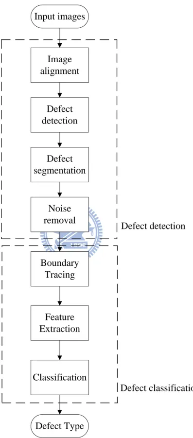
Our automatic classification system flowchart is shown in Fig. 1.1. The first module is defect detection which can find all the defects in the test image. The second module is defect classification which can classify these detected defects into their defect type.
3
Image
alignment
Input images
Defect
detection
Defect
segmentation
Noise
removal
Boundary
Tracing
Feature
Extraction
Defect Type
Classification
Defect detection
Defect classification
4
1.2 Defect Detection
Defect Detection is an important step before classifying the defects. There are two kinds of methods to detect defects which we fined. The first method is self-inspection [3] which detects the edge intrusion and protrusion then we can detect defects in the image, such as mouse bite defect. However, this method may not find all defects in the test image. The second method is image subtraction which is the most common method to detect defect. This method subtracts the test image with the reference image. The reference image is an ideal image with no defects, and the test image is an image which we want to inspect. The advantage of this method is that all defects can be found easily and the shortcoming of this method is that many noises will also be found. In our defect detection system, we choose the second method, image subtraction, to detect defects. This method can ensure that we can find out all defects in the test image.
Our defect detection algorithm can be separated into four components. The first component is the image alignment which aligns the test image with the reference image. There are many kinds of image alignment method. Gonzalez et al. [5] aligned the two difference images by calculating the correlation coefficient. Gonzalez et al. [5] also aligned the two difference images by calculating the Mean Absolute Distortion (MAD). Comparing with these two methods, calculating the MAD is more efficiency than calculating the correlation coefficient. Therefore, we apply the MAD method to align two images. The second component is the defect detection which contains image binarization and image subtraction. In order to binarize convert both the reference image and the test image into binary images, we set a threshold T After image . binarization, we subtract the binary reference image with the binary test image. Then we can acquire the missing pixel image and the excess pixel image which will be
5
detail described in Sec. 2.3.2. The third component is the defect segmentation. In order to separate the defects which are in the missing pixel image and the excess pixel image, we apply the sequential pixel marking algorithm [7] to label the connected region. Then all these defects can be separated easily. After the above process, there are many noises in the missing pixel image and excess pixel image. Therefore, the fourth component is the noise removal. Because these noises always have small size, we set a threshold num to removal these noisy pixels whose number is small than
.
num Finally, we can acquire the position and the pixel numbers of each defect.
1.3 Defect Classification
There are many kinds of defect in PCB image, but we will focus on eight kinds of defect in the thesis. These eight types of defects include “open,” “mouse bite,” “pinhole,” “missing hole,” “short,” “spur,” “missing hole” and “excess copper.” Our defect classification algorithm can be separated into three components. The first component is the boundary tracing. Boundary tracing can separate two kinds, inner boundary tracing and outer boundary tracing. Because we can know the neighboring regions state of each defect by observing the outer boundary of each defect. Therefore, we apply [8] to find the outer boundary of each defect. The second component is the feature extraction. Selecting suitable features is the most important thing on defects classification. If we can extract the more suitable feature for our defects classification system, we can classify these defects more efficiently and accurately. There are many kinds of features to identify defects. Feng et al. [3] apply the edge orientation as a feature to describe defects and Ng et al. [6] apply compactness, eccentricity and mean intensity as features to identify defects. By observing the defects, we choose the following information to be our classified features: “defect state,” “number of state
6
transition,” and “boundary state.” These features will be detailed in Sec. 3.2. The third component is the classification. Different type of defects will have different features. Therefore, we can use the above three features’ combination to classify defects efficiency.
1.4 Thesis Outline
The thesis is organized as follows. In Chapter 2, we introduce our defect detection algorithm which contains image alignment, defect detection, defect segmentation and noise removal. In Chapter 3, we describe our defect classification algorithm which contain boundary tracing, feature extraction and classification. In Chapter 4, the experiment results of our automatic defect classification systems are shown. Finally, we conclude this thesis with a discussion in Chapter 5.
7
Chapter 2 Defect Detection on Printed Circuit
Board Inner Layers
In this chapter, we will give a detail description for our defect detection system.
2.1 Overall System Architecture and Processes
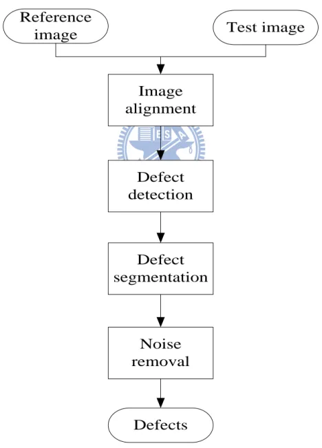
2.1.1 Non-periodic Image
For non-periodic image, we makes use of test images with difference types defects as the input images and compare them with the reference images containing no defects. First, we apply Mean Absolute Distortion [6], abbreviated as MAD, to align these two images and then we use these aligned images to the following defect detection process.
Next, we subtract these two aligned images to acquire a difference image. Because of the difference image with many noises, we apply an 5 5 average filter to the difference image to overcome this problem. Then we transfer the difference image from gray to binary with a high threshold T which can avoid too many H
noises in the image. At the same time, we also apply a low threshold T to acquire L
another binary image which can be used in the following defect repair process.
After extracting the defects, we should separate these defects into isolated defects. For this purpose, we give different label numbers to the different connecting regions in the binary image with a high threshold T , and then we can separate these H
8
Finally, in order to repair the fragmented defect region in the binary image with high threshold T , we extract the relative defect region generated by the low H
threshold T to replace the fragmented defect region. The flow chart of defect L
detection system for non-period image is shown in Fig. 2.1.
Image
alignment
Reference
image
Defect
detection
Defect
segmentation
Noise
removal
Defects
Test image
9
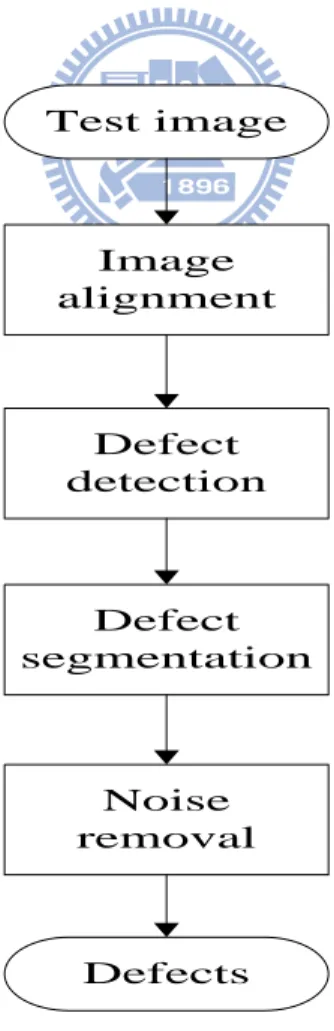
2.1.2 Periodic Image
Since periodic images have periodicity within the image, we do not have to input an extrinsic reference image but generate a new image by shifting the periodic image. In the process of image alignment, we also apply the same method, Mean Absolute
Distortion [6], abbreviated as MAD, to find the period , and then we can generate a new image by shifting the periodic image with period .
Next we use the shifted image and original test image to do the following defect detection process. In the following steps, we can use the same method with non-periodic image to detect defects. The flowchart of defect detection system for periodic image is shown in Fig. 2.2.
Image alignment Test image Defect detection Defect segmentation Noise removal Defects
10
2.2 Image Alignment
The first step of defect detection system is image alignment. Image alignment is a process to make the same object in two different images which have the same x
and y coordinate. In general, PCB images can be roughly divided to two types,
periodical and non-periodical images. Therefore, we introduce how to align non-periodic images in section 2.1.1, and how to align periodic images in section 2.1.2.
2.2.1 Non-periodic Image
For non-periodic images, we add a new reference image which is the same as the non-periodic test image but contains no defects. Therefore, image alignment for non-periodic test image is to align the test image with the reference image. Gonzales and Woods [6] used the Mean Absolute Distortion, abbreviated as MAD, to trace object’s motion, but we apply the same concept of MAD to align images. We compute four different MAD matrixes for four different cases as follows:
11
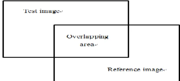
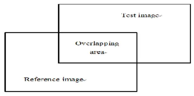
Case 1: If the reference image is on the right-lower side of the test image, as shown in Fig. 2.3.
Fig. 2.3. Reference image is on the right-lower side of test image.
Then we compute relative MAD matrix as equation (2.1). 1
0 0 1 1 0 0 1 1( , ) M N | ( , ) ( , ) | i j MAD m n r i j t i m j n MN
(2.1)where (m n is the displacement between the reference image and the test image, 0, 0)
M and N are the size of the overlapping area, t is matrix of pixels value in the test image and r is matrix of pixels value in the reference image.
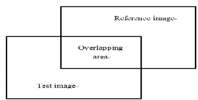
Case 2: If the reference image is on the left-upper side of the test image, as shown in Fig. 2.4.
12
Then we compute relative MAD matrix as equation (2.2). 2
0 0 1 1 0 0 1 2( , ) M N | ( , ) ( , ) | i j MAD m n r i m j n t i j MN
(2.2)where (m n is the displacement between the reference image and the test image, 0, 0)
M and N are the size of the overlapping area, t is matrix of pixels value in the test image and r is matrix of pixels value in the reference image.
Case 3: If the reference image is on the left-lower side of the test image, as shown in Fig. 2.5.
Fig. 2.5. Reference image is on the left-lower side of test image.
Then we compute relative MAD3 matrix as equation (2.3).
0 0 1 1 0 0 1 3( , ) M N | ( , ) ( , ) | i j MAD m n r i m j t i j n MN
(2.3)where (m n is the displacement between the reference image and the test image, 0, 0)
M and N are the size of the overlapping area, t is matrix of pixels value in the test image and r is matrix of pixels value in the reference image.
13
Case 4: If the reference image is on the right-upper side of the test image, as shown in Fig. 2.6.
Fig. 2.6. Reference image is on the right-upper side of test image.
Then we compute relative MAD matrix as equation (2.4). 4
0 0 1 1 0 0 1 4( , ) Mi Nj | ( , ) ( , ) | MAD m n r i j n t i m j MN
(2.4)where (m n is the displacement between the reference image and the test image, 0, 0)
M and N are the size of the overlapping area, t is matrix of pixels value in the test image and r is matrix of pixels value in the reference image.
According to the result of MAD MAD1, 2, MAD3 and MAD4, we can find the minimum value at the position ( , )x y and its corresponding situated MAD matrix.
So we acquire the direction D from test image to the reference image and the
magnitude of displacement ( x, y) between these two images. Finally, we shift the test image with the above direction D and displacement( x, y). Then the test image and the reference image will be aligned. Compare to other methods, such as normalize correlation in [5], we can align the images more efficiency.
14
2.2.2 Periodic Image
For our defect detection system, we only input a test image which has periodicity within the image. Since periodic images have periodicity within the image, we do not have to input an extrinsic reference image but generate a new image by duplicating the periodic image. However, all the defects in both the duplicated image and the periodic image have same positions, so we cannot acquire any defects by comparing these two images.
To overcome this problem, we shift the duplicated image with period to be a new image which has similar pattern but different defect positions. In order to find
, we shift the duplicated image with a pixel unit each time and compute the MAD
matrix of the test and the duplicated images in the meantime. Then we will find some values which approach 0 in the MAD matrix with a repeated interval defined as
period .
Finally, we can input this new image and the original test image to the following subtracting process, and then we can detect the defect efficiency.
2.3 Defect Detection
2.3.1 Image Binarization
We only need the boundary information of defects in the following feature extraction process, do not need intensity information of gray level, so we can decrease the complexity of images by converting both the reference and the test gray image to binary images. Therefore, we apply the same threshold T for both the reference and
15
the test image. If the pixel value is smaller than the threshold T, we define it as 0. Otherwise, we define it as 255. By doing this process, we can generate the binary reference image and the binary test image.
2.3.2 Image Subtraction
The image subtraction method is one of the common methods for defect extraction. It is simple, quick and effective in finding defects. The subtracted images can be divided into two groups: “missing pixel image,” and “excess pixel image.” The missing pixel image is composed of missing pixels which appear in the reference image but not in the test image. The missing pixel image group Missing(x, y) can be derived by Eq. (2.5).
1 (missing pixel), if ( , ) 1 ( , ) and ( , ) 0
0 (non-missing pixel), otherwise
Reference x y Missing x y Test x y (2.5)
On the contrary, the excess pixel image is composed of excess pixels which appear in the test image but not in the reference image. The excess image group
( , )
Excess x y can be derived by Eq. (2.6).
1 (excess pixel), if ( , ) 0 ( , ) and ( , ) 1
0 (non-excess pixel), otherwise Reference x y Excess x y Test x y (2.6)
After this subtracting process, we can acquire the missing pixel image and the excess pixel image. Then these binary images will be used in subsequent.
16
2.4 Defect Segmentation
In order to find the position and the size of defects, defect segmentation is a necessary process. In this step, we will deal with the missing pixel image and the excess pixel image in the meantime. Therefore, we will explain the concept of neighbor pixels in Sec. 2.4.1 and then introduce the defect segmentation method in Sec. 2.4.2.
2.4.1 Neighbors of a Pixel
A pixel p at coordinate( , )x y has four vertical and horizontal neighbors whose coordinates are given by(x1, ),(y x1, ),( ,y x y1),( ,x y1), as shown in Fig. 2.7. This set of pixels, called the 4-neighbors of p is denoted by , N p4( ). Each pixel is a unit distance from( , )x y .
17
2.4.2 Labeling of Connected Regions
To mark the connected regions, we apply the following sequential pixel marking algorithm [7]. The basic concept is to scan the whole image from left to right and from top to bottom to mark each pixel. Whenever we find a pixel which transfers from 0 to 1, we will give this pixel with a new label. But if this pixel is connected to other pixels which have been labeled, we will give this pixel a same label to its neighborhood. Next, we indicate the various situations of this algorithm.
1) If the current scanned pixel value is 0, then we omit it and process to the next pixel. 2) If the current scanned pixel value is 1, then we check its left and above pixels: (a) If both pixel values are 0, then we will give a new label to this current pixel, as
shown in Fig. 2.8;
Assign a new label
Fig. 2.8. The case of current scanned pixel value is 1 and both left and above pixel values are 0.
18
(b) If one of the left and the above pixel value is 1, then we will give the same label with this connected neighborhood to this current pixel, as shown in Fig. 2.9;
1
Label
Assign the same label with the connected neighborhood.
Fig. 2.9. The case of current scanned pixel value is 1 and one of the left and the above pixel has been labeled.
(c) If both of the left and the above pixel values are 1 and have the same label, then we will give the same label with these two neighborhood to the current pixel, as shown in Fig. 2.10;
Fig. 2.10. The case of current scanned pixel value is 1 and both the left and the above pixel have the same label.
19
(d) If both of the left and the above pixel values are 1 but have different labels, then we will give the same label with the above neighborhood to this current pixel. Then record and give these two pixels an equivalent mark, such as label 1 equal to label 2, and as shown in Fig. 2.11.
Assign the same label with the above pixel and mark label 1 equivalent to label 2
1
Label
1 1 1
2
Fig. 2.11. The current scanned pixel value is 1 and the left and the above pixel have different labels.
After this pixel-by-pixel scanning process, all isolated defects have their own labels. Then we can understand the pixel number in each defect and the position of these defects in the image.
2.5 Noise Removal
The purpose of noise removal is to remove outliers and decrease the affection of noises on defect detection. There are some noises in the missing pixel image and the
20
excess pixel image and most of these noises are small. Therefore, we apply the same threshold num for the missing pixel image and the excess pixel image to reduce the noisy pixels. In Sec. 2.4, we can acquire pixel number of all defects. Then, we compare the pixel number of all defects to this threshold num. If the pixel number of the defect is smaller than the threshold num we define it as noise. Otherwise, we , define it as a defect. After this step, most of noises can be removed from the image.
21
Chapter 3 Defect Classification on Printed Circuit
Board Inner Layers
In this chapter, we will detail explain our defect classification algorithm. The flowchart of defect classification system is shown in Fig. 3.1. In order to classify the type of defects, we will first find outer boundaries of each defect, and then extract different features from boundaries information. Therefore, we will give a detail description on boundary extraction in Sec. 3.1, then how to extract these features in Sec. 3.2, and finally the classification method in Sec. 3.3.
Defects Boundary Tracing Feature Extraction Classification Defect Type
22
3.1 Boundary Tracing
The following algorithm contains both inner boundary tracing and outer boundary tracing. An inner boundary is a subset of the region but the outer boundary is not a subset of the region.
3.1.1 Inner Boundary Tracing
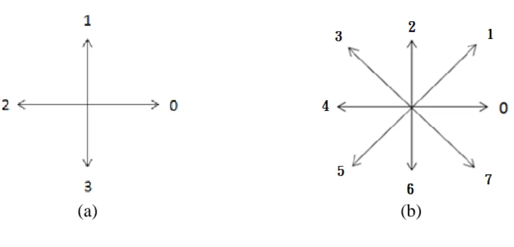
The following steps are applied by the inner boundary tracing [8].
1) Search the image from top left until a pixel of a new region is found; this pixel P then has the minimum column value of all pixels of that region 0
having the minimum row value. Pixel P is starting pixel of the region 0
boundary. Define a variable dir which stores the direction of the previous move along the boundary from the previous boundary element to the current boundary element. Assign
(a) dir3 if the boundary is defected in 4-connectivity, as shown in Fig. 3.2(a).
(b) dir7 if the boundary is defected in 8-connectivity, as shown in Fig. 3.2(b).
23
(a) (b)
Fig. 3.2. Inner boundary tracing. (a) Direction notation, 4-connectivity, (b) direction notation, 8-connectivity.
2) Search the 3 3 neighborhood of the current pixel in the counterclockwise direction, beginning the neighborhood search in the pixel positioned in the direction.
(a) (dir3) mod 4 .
(b) (dir7) mod 8 if dir is even. (d i r 6 ) mod 8 if dir is odd.
This first pixel found with the same value as the current pixel is a new boundary element P Update the dir value. n.
3) If the current boundary element P is equal to the second border element n
1,
P and if the previous boundary element Pn1 is equal to P stop. 0,
Otherwise repeat step 2).
24
3.1.2 Outer Boundary Tracing
The following steps are used by the outer boundary tracing [8]. 1) Trace the inner region boundary in 4-connectivity until done.
2) The outer boundary consists of non-region pixels that were tested during the search process; if some pixels were tested more than once, they are listed more than once in the outer boundary list.
3.2 Feature Extraction
Selecting suitable featuresis the most important thing on defects classification. If we can extract the more suitable feature for our defects classification system, we can classify these defects more efficiency and more accuracy. By observing the defects, we choose the following information to be our classified features: “defect state,” “number of state transition,” and “boundary state.”
Defect state is the first feature which is extracted by subtracting the binary reference image from the binary test image. In the process of image subtraction, we divide the subtracted image into two groups: “missing pixel image,” and “excess pixel image,” as mentioned in Sec. 2.3.2. Missing defects means the region of defects consist of the missing pixels. Correspondingly, excess defects means the region of defects consist of the excess pixels. Therefore, we can separate defects into two types, missing defects and excess defects.
Number of state transition, abbreviated as NOST, is the second feature which is extracted from the boundary of the defect. Because an inner boundary is a subset of the region, the NOST for the inner boundary of the defect is always 0. Therefore, we
25
extract the feature from the outer boundary of the defect to classify defects. It is different from every type of defects.
In order to acquire NOST, we trace the outer boundary of the defect in the counterclockwise direction. If the pixel value on the outer boundary changes from 0 to 1 or 1 to 0, the NOST will add one. After circling around the outer boundaries of all defects, we can acquire the unique NOST for each defect. Fig. 3.3 is an example of extracting NOST feature from the defect. The gray region in Fig 3.3 represents the defect, and P means the intensity of the pixel with serial number t t.
t t-1 t-2 t-3 t+1 t+2 t+3 t+4 t+5 Number of state transitions NOST NOST+1 t P Pt1 Pt2 1 t P
Fig. 3.3. The boundary of state transition of the defect.
Boundary state, abbreviated as BS, is the third feature which is also extracted from the outer boundary of the defect. Different form NOST, the BS has to record all the pixel value on the outer boundary of the defect. We trace and record all the pixel values on outer boundaries of all the defects in the counterclockwise direction, as shown in Fig. 3.4.
26
boundary state
Fig. 3.4. The boundary state of the defect.
The purpose of computing BS is to estimate the location of the defects, in other word, we can confirm that the defect is located on the pattern boundary or in the middle of pattern from BS feature. If the BS of the defect is shown as Fig. 3.5(a), the defect is located in the conductor which pixel values are 1. If the BS of the defect is shown as Fig. 3.5(b), the defect is located in the nonconductor which pixel values are 0. If the BS of the defect is shown as Fig. 3.5(c), the defect is located both on the edge of the nonconductor and the conductor. If the BS of the defect is shown as Fig. 3.5(d), the defect is across through the conductor or the nonconductor. Different defects have different BS, so we can use this feature in following defects classification process.
(a) (b) (c) (d)
Fig. 3.5. Four types of the BS. (a) Defect is located in the nonconductor, (b) defect is located in the conductor, (c) defect is located both on the edge of the nonconductor and the conductor, (d) defect across through the conductor or the nonconductor.
27
3.3 Classification Method
There are many kinds of defect in PCB image, but we will focus on eight kinds of defect in our dissertation. In our classification process, we mainly apply the method of boundary state transition [9], abbreviated as BST, to classify defects. This method can classify eight types of defects by using three features, “defect state,” “number of state transition” and “boundary state,” as mentioned in Sec. 3.2. These eight types of defects are “open,” “mouse bite,” “pinhole,” “missing hole,” “short,” “spur,” “missing hole” and “excess copper [9].” Fig. 3.6 shows these eight types of defects. The black region in Fig 3.6 represents the nonconductor region; the white region in Fig 3.6 represents the conductor region and the gray region in Fig 3.6 represents the defect.
28
After detecting defects, the first step of BST is to divide these defects into two classes, missing and excess. If defects consist of missing pixels as mentioned in Sec. 3.2, they will be classified to missing defects, such as “open,” “mouse bite,” “missing conductor,” and “pinhole,” and if defects consist of excess pixels, they will be classified to excess defects, such as “short,” “excess copper,” “spur,” and “missing hole.” Then we apply two features, NOST and BS, to classify these eight defects into their own type.
For missing defects, the open defects can be classified when the NOST is 4 and the mouse bite defects can be classified when the NOST is 2. However, the missing conductor defects and the pinhole defects have the same NOST with 0. Therefore, these two types of defects cannot be classified by using only NOST feature. To overcome this problem, we add another feature, BS, to separate the missing conductor defect and the pinhole defect, due to the BS of missing conductor defects are all 0 and the BS of pinhole defects are all 1. Therefore, we can classify these four missing defects by using NOST and BS features to their own type. Fig. 3.7 is the flowchart of using NOST and BS feature to classify four missing defects to their own type.
29
For excess defects, the short defects can be classified when the NOST is 4 and the spur defects can be classified when the NOST is 2. However, the excess copper defects and the missing hole defects have the same NOST with 0. Therefore, these two types of defects cannot be classified by using only NOST feature. To overcome this problem, we also add another feature, BS, to separate the excess copper defect and the missing hole defect, duo to the BS of excess copper defects are all 0 and the BS of missing hole defects are all 1. Therefore, we can classify these four excess defects by using NOST and BS features to their own type. Fig. 3.8 is the flowchart of using NOST and BS feature to classify four excess defects to their own type.
Fig. 3.8. The flowchart of classifying four excess defects.
Finally, we combine the result of both missing defects and excess defects, and then we can classify all these eight types of defects.
30
Chapter 4 Experimental Results
In our experiment, we create some synthetic images to test whether that our system is really working out or not. The image resolutions of these synthetic images are 512 512 pixels. However, the synthetic images are sharper than the real PCB images. Therefore, we apply the average filter to blur the synthetic images. If we apply the average filter with larger size, the synthetic image we generated will be much vaguer.
4.1 Defect Detection
Our defect detection is focus on how to segment defects from images. If we can segment the defects more precisely, we can classify defects more correctly. PCB images can be roughly divided into two types, periodical and non-periodical images. Therefore, we will discuss the result of defect detection with the non-periodical image in Sec. 4.1.1 and the periodical in Sec. 4.1.2.
4.1.1 Non-periodic Image
For non-periodic images, we have two images in the input, reference image and test image to find defects. The reference image is an ideal image with no defects, and the test image is a synthetic image which we put eight types of defects described in Chapter 3 in the test image generated. These eight types of defects are “open,” “mouse bite,” “pinhole,” “missing conductor,” “short,” “spur,” “missing hole,” and “excess copper.” To generate synthetic images to be more similar to the real PCB images, since the synthetic images are sharper than the real PCB images, we apply an
31
7 7 average filter with every entry having value 1
49 on the synthetic images. The synthetic reference image and the synthetic test image are shown in Fig. 4.1(a) and Fig. 4.1(b), respectively. On the other hand, the blurred reference image and blurred test image, are shown in Fig. 4.1(c) and Fig. 4.1(d), which are blurred by 7 7
average filter.
(a) (b)
(c) (d)
Fig. 4.1. The synthetic images. (a) The synthetic reference image. (b) The synthetic test image. (c) The synthetic reference image which is blurred by 7 7 average filter. (d) The synthetic test image which is blurred by 7 7 average filter.
32
Image alignment is the first step to detect the defects. Therefore, we have to align the test images to the reference image, as shown in Fig. 4.1(c) and Fig. 4.1(d). The result of image alignment is shown in Fig. 4.2. In this case, we can find the displacement ( x, y) between these two images is (10, 10) and the reference image is on the left-upper side of the test image, according to the method mentioned in Sec. 2.2.1.
(a) (b)
Fig. 4.2. The result of image alignment. (a) The aligned reference image. (b) The aligned test image.
After aligning the test image with the reference image, the next step is to segment defects from images. We apply the same threshold T 128 to the aligned reference image and the aligned test image to acquire the binary reference image and binary test image, as shown in Fig. 4.3(a) and Fig. 4.3(b), respectively. Then we subtract the reference image from the test image producing the excess pixel image of
33
positive pixel difference and producing the missing pixel image of negative pixel difference as shown in Fig. 4.3(c) and Fig. 4.3(d). However, these two images may contain many noisy pixels thus we apply the minimal connected threshold of 10 to reduce the noisy pixels. Namely, if the pixel numbers of the connected region is less than 10 pixels, this region will be defined as noise, as mentioned in Sec. 2.5. Finally, we can obtain two clear images, clear missing pixel image and clear excess pixel image, as shown in Fig. 4.3(e) and Fig. 4.3(f), respectively.
(a) (b)
34
(e) (f)
Fig. 4.3. The result of defect detection. (a) The binary reference image. (b) The binary test image. (c) The missing pixel image. (d) The excess pixel image. (e) The clear missing pixel image. (f) The clear excess pixel image.
At the end of defect detection, we record the left-upper coordinates, number of pixels and trueness of each defect blob. Table I and Table II show the defect detection result of clear missing pixel image and clear excess pixel image.
TABLE I
THE DEFECT DETECTION RESULT OF MISSING PIXEL IMAGE
Left-upper coordinates of defect blob Defect index
x y number of pixels in
defect blob defect trueness 1m 102 105 362 True 2m 140 152 344 True 3m 210 207 317 True 4m 328 94 327 True
35
TABLE II
THE DEFECT DETECTION RESULT OF EXCESS PIXEL IMAGE
Left-upper coordinates of defect blob Defect index
x y number of pixels in
defect blob defect trueness 1e 39 141 100 True 2e 79 84 110 True 3e 141 119 813 True 4e 303 147 398 True
4.1.2 Periodic Image
For periodic images, we only have to input a test image to find the defects, as shown in Fig. 4.4(a). This test image is also a synthetic image and filtered by 7 7
average filter. Therefore, we apply the method of MAD, as mentioned in Sec. 2.2, to find out the period ( x, y)(50,128). Then we left shift the test image with period
50 x
to generate the new reference image. Fig. 4.4 shows the result of image alignment in test image.
36
(c)
Fig. 4.4. The result of image alignment. (a) The test image. (b) The new reference image with left shifting period x50 (c) The aligned test image.
After acquiring the reference image, we also apply the image subtraction method to detect defects. We apply the same threshold T 128 for aligned reference image and aligned test image and then we can acquire the binary reference image and binary test image, as shown in Fig. 4.5(a) and Fig. 4.5(b). After that, we subtract these two images to generate the missing pixel image and the excess pixel image, as shown in Fig. 4.5(c) and Fig. 4.5(d). In Fig. 4.5(c) and Fig. 4.5(d), we can detect defects but could also contain noisy pixels. Therefore, we apply the threshold num10 to reduce the noisy pixels, as mentioned in Sec. 2.5. Finally, we can obtain two clear image, clear missing pixel image and clear excess pixel image, in Fig. 4.5(e) and Fig. 4.5(f).
37
(a) (b)
(e) (f)
(c) (d)
Fig. 4.5. The result of defect detection. (a) The binary reference image. (b) The binary test image. (c) The missing pixel image. (d) The excess pixel image. (e) The clear missing pixel image. (f) The clear excess pixel image.
38
Table III and Table IV show the defect detection result of clear missing pixel image and clear excess pixel image. Different from non-periodic images, the reference image of periodic image is generated by left shifting the test image with period x50, so the reference and the test image of periodic image have the same number but the different location of the defects. Hence, we can observe that the total number of defects in both missing pixel image and excess pixel image is sixteen not eight, as shown in Table III and Table IV.
TABLE III
THE DEFECT DETECTION RESULT OF MISSING PIXEL IMAGE
Left-upper coordinates of defect blob Defect index
x y number of pixels
in defect blob defect trueness
1m 51 300 320 True (Caused by periodical) 2m 161 424 260 True (Caused by periodical) 3m 171 66 410 True 4m 208 176 19 True (Caused by periodical) 5m 243 307 200 True 6m 305 52 85 True 7m 356 273 84 True (Caused by periodical) 8m 379 418 156 True
39
TABLE IV
THE DEFECT DETECTION RESULT OF EXCESS PIXEL IMAGE
Left-upper coordinates of defect blob Defect index
x y number of pixels
in defect blob defect trueness 1e 101 300 320 True 2e 121 66 410 True (Caused by periodical) 3e 193 307 200 True (Caused by periodical) 4e 211 424 260 True 5e 255 52 85 True (Caused by periodical) 6e 258 176 19 True 7e 329 418 156 True (Caused by periodical) 8e 406 273 84 True
4.2 Defect Classification
In our classification method, we apply the method of boundary state transition [10] to classify the eight types of defects: “open,” “mouse bite,” “pinhole,” “missing conductor,” “short,” “spur,” “missing hole,” and “excess copper.” We will discuss the classification result of the periodical image in Sec. 4.2.1 and the non-periodical in Sec. 4.2.2.
4.2.1 Non-periodic Image
After detecting defects, we can acquire the clear missing pixel image and the clear excess pixel image, as shown in Fig. 4.6(a) and Fig. 4.6(b). In order to classify
40
the type of each defect, we extract the three features, “defect state,” “boundary state,” and “number of state transition,” from the outer boundary of each defect. Therefore, we have to extract the boundary of each defect at first, as shown in Fig. 4.6(c) and Fig. 4.6(d).
(a) (b)
(c) (d)
Fig. 4.6. The result of defect classification. (a) The clear missing pixel image. (b) The clear excess pixel image. (c) The outer boundary of the clear missing pixel image. (d) The outer boundary of the clear excess pixel image.
41
After acquiring the boundaries of each defect in both the clear missing pixel image and the clear excess pixel image, we can extract the feature of each defect and then classify these defects into their own type, as mentioned in Sec. 3.3. After classifying all these defects, we will record the left-upper coordinates, NOST, BS and defect type of each defect. Table V and Table VI show the classification result of clear missing pixel image and clear excess pixel image. In Table VI, we can observe that there is an unknown defect type. The reason is that in our defect detection algorithm, we only use a threshold T to acquire the binary reference image and the
test reference image. However, using the same threshold T to binarize whole images
could not be suitable for each defect in the reference image and test image. Therefore, we acquire the wrong NOST 8 and misclassification in this case.
TABLE V
THE DEFECT CLASSIFICATION RESULT OF MISSING PIXEL IMAGE
Left-upper coordinates of defect blob Defect index
x y NOST BS defect type
1m 102 105 4 Open
2m 140 152 0 Pinhole
3m 210 207 2 Mouse bite
42
TABLE VI
THE DEFECT CLASSIFICATION RESULT OF EXCESS PIXEL IMAGE
Left-upper coordinates of defect blob Defect index
x y NOST BS defect type
1e 39 141 0 Excess copper 2e 79 84 8 Unknown (Missing hole) 3e 141 119 4 Short 4e 303 147 2 Spur
4.2.2 Periodic Image
For periodic image, we apply the same classification method as non-periodic image used. We also extract the outer boundary of each defect, as shown in Fig. 4.7.
43
(c)
(d)
Fig. 4.7. The result of defect classification. (a) The clear missing pixel image. (b) The clear excess pixel image. (c) The outer boundary of the clear missing pixel image. (d) The outer boundary of the clear excess pixel image.
After acquiring the boundaries of each defect in both the clear missing pixel image and the clear excess pixel image, we can extract the feature of each defect and then classify these defects into their own type, as mentioned in Sec. 3.3. Table VII and Table VIII show the classification result of clear missing pixel image and clear excess pixel image. In Table VIII, we can observe that there is a misclassification defect. The reason is that in our defect detection algorithm, we only use a threshold
T to acquire the binary reference image and the test reference image. However, using
the same threshold T to binarize whole images could not be suitable for each defect
in the reference image and test image. Therefore, the regions of the defects are not very correct and then cause the wrong NOST and misclassification.
44
TABLE VII
THE DEFECT CLASSIFICATION RESULT OF MISSING PIXEL IMAGE
Left-upper coordinates of defect blob Defect index
x y NOST BS defect type
1m 51 300 4 Open (Caused by periodical) 2m 161 424 2 Mouse bite (Caused by periodical) 3m 171 66 4 Open 4m 208 176 2 Mouse bite (Caused by periodical) 5m 243 307 2 Mouse bite 6m 305 52 0 Missing conductor 7m 356 273 0 Missing conductor (Caused by periodical) 8m 379 418 0 Pinhole TABLE VIII
THE DEFECT CLASSIFICATION RESULT OF EXCESS PIXEL IMAGE
Left-upper coordinates of defect blob
Defect index
x y NOST BS defect type
1e 101 300 4 Short
2e 121 66 4 Short (Caused by periodical) 3e 193 307 2 Spur
45 4e 211 424 2 Spur 5e 255 52 0 Excess copper (Caused by periodical) 6e 258 176 2 Spur (Missing hole) 7e 329 418 0 Missing hole (Caused by periodical) 8e 406 273 0 Excess copper
46
Chapter 5 Conclusion
In this thesis, we implement the automatic defect classification system which contains the defect detection and the defect classification. In our defect detection algorithm, we apply the image subtraction method to find defects. At first, we apply MAD to align the reference image with test image. Then we converted the subtracted images into the binary images by setting a threshold T After acquiring these binary . images, we subtracted the binary reference image with the binary test image, and then we removed the noises by setting a threshold num Finally, we can detect all defects . in the test image.
For defect classification, we traced the outer boundary of each defects and then extracted the features from the outer boundaries. These features include “defect state,” “number of state transition,” and “boundary state.” By these features, we can classify the types of defects. After the above process, all defects can be detected and classified efficiency.
Experimental results have shown that our automatic defect classification system can work well and have good performance. In the future, we intend to enhance the capability of our automatic defect classification system to classify more defect types. Moreover, we will extend our system on the scanning electron microscope (SEM) images.
47
References
[1] C. H. Wang, W. Kuo, and H. Bensmail, “Detection and classification of defect patterns on semiconductor wafers,” IIE Trans., vol. 39, no. 12, pp. 1059–1068, 2006.
[2] F. L. Chen and S. F. Liu, “A neural-network approach to recognize defect spatial pattern in semiconductor fabrication,” IEEE Trans. Semiconductor
Manufacturing, vol. 13, pp. 366–373, Aug. 2000.
[3] H. Feng, J. Ye, and R. F. W. Pease, “Self-inspection of IC pattern defects,”
Journal of Vacuum Science & Technology, vol. 22, pp. 3386–3389, Nov. 2004.
[4] M. Luria, M. Moran, D. Yaffe, and J. Kawski, “DCS-1: A fuzzy logic expert system for automatic defect classification of semiconductor wafer defects,” in
Proc. 3rd IEEE Conf. Fuzzy Syst.—Part III, vol. 3, pp. 2100–2106, 1994.
[5] R. Gonzales and R. Woods, Digital Image Processing, 3rd ed. Pearson Education International, pp. 589–591, 2008.
[6] A. N. Ng, E. Y. Lam, R. Chung, K. S. Fung, and W. H. Leung, “Reference-free detection of semiconductor assembly defect,” in Proc. SPIE, vol. 5679, pp. 27– 35, 2005.
[7] H. Feng, J. Ye, and R. F. W. Pease, “Reconstruction of pattern images from scanning electron microscope images,” Journal of Vacuum Science &
Technology, vol. 23, pp. 3080–3084, 2005.
[8] M. Sonka, V. Hlavac, R. Boyle, Image Processing, Analysis, and Machine
Vision, 3rd ed. International Student Edition, pp. 191–193, 2008.
[9] H. Rau, C.H. Wu, “Automatic optical inspection for detecting defects on printed circuit board inner layers,” International journal of manufacturing
48
[10]S. F. Liu, F. L. Chen, and W. B. Lu, “Wafer bin map recognition using a neural network approach,” Int. J. Production Res., vol. 40, no. 10, pp. 2207–2223, 2002.
[11] P. B. Chou, A. R. Rao, M. C. Sturzenbecker, F. Y. Wu, and V. H. Brecher, “Automatic defect classification for semiconductor manufacturing,” Mach.
Vision Applicat., vol. 9, no. 4, pp. 210–214, 1997.
[12] A. Ben-Porath, T. Hayes, and A. Skumanich, “Advanced process development and control based on a fully automated SEM with ADC,” in Proc. Advanced
Semiconductor Manufacturing Conf., pp. 275–280, 1999.
[13] R. L. Guldi, “In-line defect reduction from a historical perspective and its implications for future integrated circuit manufacturing,” IEEE Trans. Semicond.
Manuf., vol. 17, no. 4, pp. 629–640, Nov. 2004.
[14] Honda, Toshifumi, et al. “Fuzzy selective voting classifier with defect extraction based on comparison within an image,” International Symposium on
Multispectral Image Processing and Pattern Recognition. International Society
for Optics and Photonics, 2007.
[15] Gleason, Shaun S., et al. “Detection of semiconductor defects using a novel fractal encoding algorithm,” Design, Process Integration, and Characterization
for Microelectronics. International Society for Optics and Photonics, 2002.
[16] H. Feng, J. Ye, and R. F. Pease, “Self-inspection of integrated circuits pattern defects using support vector machines,” Journal of vacuum & science technology, vol. 23, no. 6, pp. 3085–3089, Nov. 2005.