國
立
交
通
大
學
光電工程研究所
碩
士
論
文
整合多模梯形波導之多模干涉矽波導線交錯元件的
研究
Study of multimode interference-based waveguide crossings
integrated with multimode tapers for silicon wire waveguides
研 究 生:邱家祥
指導教授:陳瓊華 教授
整合多模梯形波導之多模干涉矽波導線交錯元件的研究
Study of multimode interference-based waveguide crossings
integrated with multimode tapers for silicon wire waveguides
研 究 生:邱家祥 Student:Chia-Hsiang Chiu
指導教授:陳瓊華 Advisor:Chyong-Hua Chen
國 立 交 通 大 學
光電工程研究所
碩 士 論 文
A ThesisSubmitted to Department of Photonics & and Institute of Electro-Optical
College of Electrical Engineering
National Chiao Tung University
in partial Fulfillment of the Requirements
for the Degree of
Master
in
Electro-Optical Engineering
June 2010
Hsinchu, Taiwan, Republic of China
i
整合多模梯形波導之多模干涉矽波導線交錯元件的研究
學生:邱家祥 指導教授:陳瓊華 博士
國立交通大學 光電工程研究所
摘
要
在本論文中,我們使用微型化之多模梯形波導設計出一新穎之多模干涉矽波導交錯 結構並且使用時域有限差分法模擬其光學特性。此微型化的梯形波導有效地將入射光場 擴束,因此除了降低輸入(輸出)波導與多模干涉波導之間的傳輸損耗,並且減少在波導 交錯位置所產生的串音干擾 (Crosstalk)。此外,微型化梯型波導的使用促使縮短於多模 干涉波導產生自我成像的所需之距離,進而減小交錯結構所需之多模干涉波導長度少於 兩倍的拍長。利用三維時域有限差分法,我們探討不同梯形波導及形狀對於多模干涉交 錯結構的特性影響並且獲得一個整合寬度平方變化梯型波導的多模干涉波導交錯結 構,其尺寸為 5800 × 5800 平方奈米,在 1550 奈米的波長下的插入損耗 為 0.15 分貝 及串音干擾為 -42 分貝,並且擁有於 1500 奈米到 1600 奈米波段下的寬頻穿透頻譜。
ii
Study of multimode interference-based waveguide crossings integrated with
multimode tapers for silicon wire waveguides
Student : Chia-Hsinag Chiu Advisor : Dr. Chyong-Hua Chen
Institute of Electro-Optical Engineering
National Chiao Tung University
Abstract
Novel multimode-interference (MMI)-based crossings integrated with miniaturized
tapers are numerically presented for Silicon wire waveguides. These miniature tapers function
as field expanders to reduce transition loss between the input/output waveguide and the MMI
waveguide and the crosstalk in the crossing region. As a consequence, the lengths of MMI
waveguide reduce to less than twice of the beat length. Using finite difference time domain
method, we demonstrate that the MMI-based waveguide crossing embedded in the quadratic
tapers has the size of 5800×5800 nm2, the insertion loss of 0.15 dB and the crosstalk of -42 dB
at the wavelength of 1550 nm and broad transmission spectrum ranging from 1500 nm to
iii
誌謝
在碩士的生涯中,雖然只有短短的兩年,但在這期間也發生了很多事,讓我對許多 事情有了新的體悟,也要感謝許多人的支持與幫忙,讓我能夠順利的完成碩士學位。首 先我要感謝的就是我的指導老師陳瓊華教授,她是一位研究認真且為學生著想的好教 授,老師除了在研究方面給我紮實的訓練與指導外,也跟我分享了很多人生的寶貴經 驗,讓我在各個方面都獲益良多。 再來我要感謝李柏璁教授、鄒志偉教授、何符漢博士能夠抽空來擔任我的碩士學位 口試委員,並給予我在研究上的指導與肯定。還要感謝實驗室的各個成員,有洪瑋倫學 長跟我分享在碩士班的經驗才讓我知道如何處理碩士班的事物,有侯紹璿學長跟我一起 研究模擬軟體才能順利完成研究,還有感謝范日華可以跟我一起發洩壓力,感謝郁欣姐 跟我一起闖過口試的難關,還有感謝翁一正幫忙處理實驗室的大小事,還有感謝唯一跟 我同屆的同學游文宏曾經陪我在碩一上一同修課。 還有要感謝紹平跟瑞泰一起接引我加入如來精舍,讓我能在妙禪師父的帶領下修 行,還有感謝德正學長跟我分享禪行的心得解開我對禪修的疑惑,感謝妙禪師父的帶 領,讓我在心情上能夠比較平靜,讓一切隨順圓滿。 再來要感謝我的家人對我的支持,讓我隨時有個溫暖的家可以依靠。最後我要感謝 傑尼,在這一路以來,因為有你的支持與包容,我才能夠勇敢去面對所有遇到的難關, 希望在人生未來的路上,我們能一起繼續走下去。iv
Content
Abstract (Chense version)
... i
Abstract (English version)
... ii
Acknowledgement
... iii
Content
... iv
List of Figure
... v
List of table
... vi
Chapter 1 Introduction
... 1
1.1 Photonic Integrated Circuits and Silicon Photonics
... 1
1.2 Waveguide crossing
... 2
1.2.1 Mode expander waveguide crossing
... 4
1.2.2 Double etched mode expander waveguide crossing
... 5
1.2.3 Highly efficient mode expander waveguide crossing
... 6
1.2.4 Metamaterial filled waveguide crossing
... 7
1.2.5 Multimode-interference-based waveguide crossing
... 8
1.3 Organization
... 9
Chapter 2 Theories
... 10
2.1 Self-imaging principle
... 10
2.2 Eigenmode expansion method for tapers
... 13
2.2.1 Single-mode tapers
... 13
2.2.2 Multimode tapers
... 17
Chapter 3 Design approach
... 20
3.1 Structure of the designed MMI based waveguide crossing
... 20
3.2 Eigenmode properties of the input/output and MMI waveguides
... 22
3.3 Diffraction loss with different self-image profiles
... 28
3.4 Multimode taper design
... 32
3.4.1 Effect of taper length on the amplitude ratio
η
... 35
3.4.2 Effect of taper length on transition loss
... 36
3.4.3 Effect of taper length on the effective beat length
... 38
3.5 Performances of MMI based crossings with linear tapers
... 40
3.6 Effect of the Taper Profiles
... 43
3.7 Wavelength dependence on insertion loss and crosstalk
... 47
Chapter 4 Conclusion
... 48
v
List of Figure
Figure 1.2-1 The diagram of a photonics circuits...2
Figure 1.2-2 The direct waveguide crossing and the corresponding field
distribution...3
Figure 1.2-3 The mode expandr waveguide crossing and the corresponding
field distribution...4
Figure 1.2-4 The double etched waveguide crossing and the corresponding
field distribution...5
Figure 1.2-5 The Highly efficient waveguide crossing and the corresponding
field distribution...6
Figure 1.2-6 The metamaterial filled waveguide crossing and the
corresponding field distribution...7
Figure 1.2-7 The MMI-based waveguide crossing and the corresponding field
distribution...8
Figure 2.1-1 The periodic intensity distribution is formed along the
propagating direction...12
Figure 2.2-1 a taper is divide into several waveguide sections...14
Figure 2.2-2 a multimode taper is divided into a series of individual
waveguides with fixed width. Each section of the individual
waveguide can be expressed by a transfer matrix P
mdescribing
the amplitude variations of the forward and backward
propagating modes at two adjacent sections...17
Figure 3.1-1 Schematic structure of the proposed waveguide crossing...21
Figure 3.2-1 The cross-section of designed input/output waveguides...22
Figure 3.2-2 The fundamental mode profile of the input and output
waveguide...23
Figure 3.2-3 The TE
00mode distribution of the MMI waveguide...25
Figure 3.2-4 The TE
01mode distribution of the MMI waveguide...26
Figure 3.2-5 The TE
02mode distribution of the MMI waveguide...27
Figure 3.3-1 Diffraction loss as a function of amplitude ratio η...29
Figure 3.3-2 Variations of field distributions normalized by the power of the
self-image at amplitude ratio
η of (a) 0.007(b) 0.18 (c) 0.27 and
(d) 0.51...31
Figure 3.4-1 The diagram of a multimode taper...32
Figure 3.4-2 Evolution of the input guided mode propagation through the
vi
nm and the MMI waveguide...34
Figure 3.4-3 Variation of taper length on the amplitude ratio...35
Figure 3.4-4 Transition loss as a function of the taper length...37
Figure 3.4-5 Effective beat length L
effas a function of the taper length L
t...38
Figure 3.5-1 FDTD simulations of the input guided mode propagation through
MMI-based waveguide crossings sandwiched by four identical
linear tapers with (a) L
t=0 and L
m=4543.4 nm, (b) L
t=560 nm and
L
m=3778.5 nm, (c) L
t=1000 nm and L
m=3600 nm and (d)
L
t=2000 nm and L
m=3450.4 nm...42
Figure 3.6-1 Evolution of the input guided mode propagation through different
taper profiles with n= (a) 0.25, (b) 0.5, (c) 1 and (d) 2 and the
MMI waveguide... ...44
Figure 3.6-2 FDTD simulations of the input guided mode propagation through
MMI-based waveguide crossings sandwiched by four different
tapers with (a) L
t=750nm and n=0.25, (b) L
t=530 nm and n=0.5,
(c) L
t=560 nm and n=1 and (d) L
t=1000 nm and
n=2...45
Figure 3.7 (a) Simulated insertion loss spectra and (b) calculated crosstalk
spectra of the designed MMI-based waveguide crossings for
n=0.25 (black curves), 0.5 (red curves), 1 (blue curves) and 2
(green curves)... ...47
List of table
Table 1 Properties of MMI waveguide crossings integrated with linear
tapers at the wavelength of 1550 nm...42
Table 2 Performance of waveguide crossings with different taper profiles
at the wavelength of 1550 nm...45
1
Chapter 1 Introduction
1.1 Photonic Integrated Circuits and Silicon Photonics
In recent years, photonic integrated circuits (PICs) have attracted much attention due to
the potential for replacing the integrated circuits (ICs) to achieve high speed and broad band
data transmission. The basic optical components to implement a PIC include light sources,
optical waveguides, modulators, and photodetectors, and they can be fabricated from a variety
of materials like LiNbO3, GaAs, InP, and silicon.
Silicon is conventionally used as a substrate for integrated circuits and recently Silicon
photonics-an active research to realize photonic systems by using relatively cheap and
abundant silicon as an optical medium-provides a platform for integrating electrical circuits
and photonic circuits on a single chip. In addition, optical components made on a silicon on
insulator[1] provides the advantages of low cost and small size due to being compatible with
well-established CMOS fabrication techniques and high refractive-index contrast between
silicon and silica.
Several high performance optical components for silicon photonics[2-3] have already
presented in recent years. Low-loss silicon photonic wire waveguide had already studied with
loss 0.5dB/cm [4-5]. The silicon modulator with 10 gigabits per second (10 Gbps) was
2
Gbps data rate was presented by Intel [7]. To carry out monolithic optical integrated circuits,
the difficulty in using silicon is silicon is an indirect bandgap material so as not to emit light.
However, this issue was solved in 2005. A continuous wave silicon laser based on Raman
scattering effect [8-9] was present by Intel. Because the light source issue was solved, silicon
photonics is a promising candidate for the future computer industry.
1.2 Waveguide crossing
In PICs, waveguides are used to transit the optical signals among different optical
components. When the waveguides are crossed, the optical signals are not affected by those in
the other waveguides. As a result, the photonics circuits can be designed with grid-cross array
and manufactured monolithically, as shown in Figure 1.2-1.
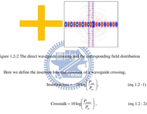
3
As shown in Fig. 1.2-1, the waveguide crossings are indispensable for efficiently using
the area of the substrate. However, in a direct waveguide crossing (i.e. two single-mode
waveguides are 90° crossed), the field diverges and leaks at the crossing region because of high index-constrast between silicon and SiO2.
Figure 1.2-2 The direct waveguide crossing and the corresponding field distribution
Here we define the insertion loss and crosstalk of a waveguide crossing,
1) -1.2 (eq. , log 10 loss Insertion − = in out P P 2) -1.2 (eq. , log 10 Crosstalk = in noise P P
where Pin is the power before entering the waveguide crossing, Pout is the power after
propagating through the waveguide crossing, and Pnoise is the power radiating into the
orthogonal waveguide. The insertion loss of a direct crossing is 1.2 dB and its crosstalk is
about -12 dB. In order to improve the performance of waveguide crossings, serveral structures
4
1.2.1 Mode expander waveguide crossing
The common structure of a waveguide crossing is a mode-expander waveguide crossing
[10]. The mode expander expands the field wide to reduce the wide-angle components of the
guided mode, thereby decreasing the diffraction of the field at the crossing region. The
schematic structure and its field distribution are shown in Figure 1.2-3. The literature shows
that the insertion loss is around 0.2 dB with its total length larger than 10 μm.
5
1.2.2 Double etched mode expander waveguide crossing
The mode expander waveguide crossing with double etched was presented in 2007 [11]
to reduce the size of this type waveguide crossing. Its structure and corresponding field
distribution are displayed in Figure 1.2-4. The insertion loss is about 0.16 dB and its total
size decreases to 6μm. However, double etched processes are required to realize this design and, as a result, the fabrication of this waveguide crossing becomes difficult and expensive,
6
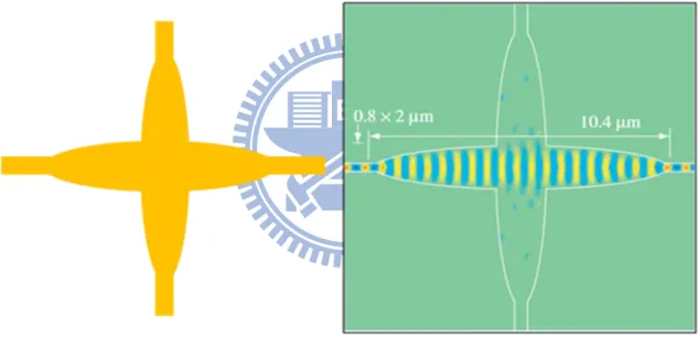
1.2.3 Highly efficient mode expander waveguide crossing
Highly efficient mode expander waveguide crossing [12] is a mode expander waveguide
crossing without double etched processes. The total size is 6×6 μm2 and the insertion loss is around 0.2 dB. Although this structure doesn't need to be fabricated by using double etched
processes, the profile of this crossing is optimized by using genetic algorithm and becomes
complex for the CMOS fabrication. In addition, the footprint of this design is still occupied
by 6×6 μm2, as shown in Figure 1.2-5.
Figure 1.2-5 The highly efficient mode expander waveguide crossing and the corresponding field distribution
7
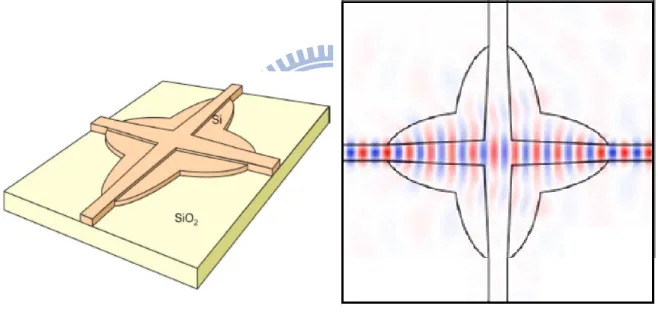
1.2.4 Metamaterial filled waveguide crossing
This waveguide crossing is filled metamaterial in the crossing region with impedance
match [13] as displayed in Figure 1.2-6. The field passes though the crossing region without
reflecting from the interface between input waveguide and crossing region because large
refractive index of the metamaterial is used to confine the light at the metamaterial-filled
crossing region. The insertion loss of this waveguide crossing is 0.04 dB and the total size is
600×600 nm2. Although Ultra-low loss and ultra-small size can be achieved in this design,
fabrication of this structure is difficult and expensive.
Figure 1.2-6 The metamaterial filled waveguide crossing and the corresponding field distribution
8
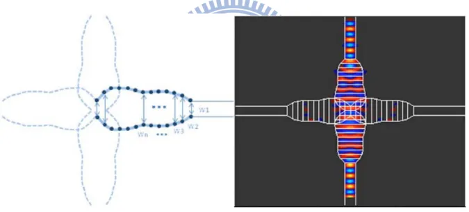
1.2.5 Multimode-interference-based waveguide crossing
Figure 1.2-7 shows the field propagates along a multimode-interference (MMI)-based
waveguide crossing and we can observe a narrowing field at the crossing region [14-15]. Due
to suppressing the field divergence at the crossing region, the insertion loss is reduced to
around 0.2 dB. The total size of MMI-based crossing is 13×13 μm2 and this size is too large to implement compact PICs.
Figure 1.2-7 The MMI-based waveguide crossing and the corresponding field distribution
All the structures of waveguide crossings mentioned above have the problems of large
footprints and complex fabrication processes. Here, we would like to present a novel
MMI-based waveguide crossing with low insertion loss and small size. In addition, the
requirement of fabrication techniques is compatible with current standard CMOS fabrication
9
1.3 Organization
The organization of this thesis is described as follows. First, we introduce the mode
expansion method for MMI waveguide and tapers in chapter 2. Next, the design approach to
design a compact, low insertion loss and small crosstalk MMI based waveguide crossing is
10
Chapter 2 Theories
In this chapter, we introduce the concept of the self-image principle which is the
fundamental mechanism to design a MMI-based waveguide crossing. Next, the mode
expansion method is presented for designing single-mode and multimode tapers.
2.1 Self-imaging principle
Self-imaging principle is the phenomenon that the field formed periodically in a multimode waveguide. In a multimode waveguide, there are several modes in this waveguide
with their mode profiles and propagation constants. As some arbitrary field is impinged into
the multimode waveguide, more than one mode are excited and each mode interfere to each
other during propagating along the multimode waveguide, resulting in periodic
multimode-interference distributions along the propagating direction. This kind of the
multimode waveguide is called the MMI waveguide.
When an arbitrary field Ein(x,y) is incident into a MMI waveguide, the field profile
Ein(x,y) can be decomposed into several modal field distributions TEi(x,y) which are the
eigenmodes of the MMI waveguides and given by
( )
, (eq.2-1) ) , ( 0∑
= = N i i i in x y CTE x y Ewhere Ci is the modal coefficient of the mode field distribution TEi(x,y), i=0..N, and
11
( )
( )
, ( , ) (eq.2-2) ) , ( ,∫∫
∫∫
= dxdy y x TE y x TE dxdy y x TE y x TE C i i i in iThe electrical filed at the arbitrary position z in a MMI waveguide is
(
)
(eq.2-3) exp ) , , ( 0 z i E T C z y x E i i N i i − β =∑
=where z is propagating direction and βi is the propagation constant of the mode field TEi(x,y).
When the field E(x,y,z) propagates along the waveguide direction z, the phase difference are
induced among different modes because each mode has different propagating constant. The
phase difference between modes changes from 0 to 2π, and the field profile E(x,y,z) in x-y plane at some distance z becomes the same as the incident field Ein as the phase difference
becomes 2mπ, m is an integer. This phenomenon is named self-imaging principle[16] in the MMI waveguide.
Here, we give an example of the self-imaging principle in a three-mode supported MMI
waveguide. Assume the incident field is the fundamental mode of an narrower waveguide,
with centrosymmetric profile. From eq. 2-1, the input field Ein(x,y) can be expressed by the
two even modes of this three-mode supported MMI waveguide. By using overlap integral,
the modal coefficient C0 and C2 for these lowest two even modes are obtained. Accordingly,
the field E(x,y,z) in the MMI waveguide can be written
(
, ,)
( , )exp(
)
( , )exp( ) (eq.2-4)
E x y z =C0TE0 x y −iβ0z +C2TE2 x y −iβ2z
where βi is the propagation constant of the mode field TEi(x,y), i=0 and 2.
12
find the self-image reformed between some specific distance periodically. This specific
distance is defined as beat length LB. In this example, the beat length can be calculated by
5) -2 (eq. 2 2 0 β β π − = B L
The field distriution of field E(x,y,z=mLB) at mutliple beat length is simplified as
(
)
(
)
(
)
[
]
{
}
(
)
{
}
6) -2 (eq. ) 0 , , ( ) , ( ) , ( ) exp( ) , ( 2 exp ) , ( ) exp( ) , ( exp ) , ( ) exp( ) , ( exp ) , ( , , 2 2 0 0 2 2 2 2 0 2 0 0 0 2 2 2 2 0 0 0 2 2 2 0 0 0 = = + = − × + − × − − = − × + − − = − + − = = z y x E y x E C y x E C L i y x E C i y x E C L i y x E C L i y x E C L i y x E C L i y x E C L z y x E B B B B B B β β β π β β β β β β βAt multiple beat length, the phase difference between the two even modes becomes 2mπ, and ,as a resulting, the field at z = 0 and the field at multiple beat length are the same, as
shown in Figure 2.1-1.
13
2.2 Eigenmode expansion method for tapers
In the following section, we introduce the analysis of tapers by using eigenmode
expansion method. Two types of the tapers are discussed- one is the single-mode taper and the
other is the multimode taper. When the light propagates through the single-mode taper, the
power of light is coupled from the input fundamental mode into the fundamental mode of
another waveguide without converting to any higher-order modes of waveguides along the
taper. When the light propagates through the multimode taper, the power is coupled into the
fundamental mode and the other high modes of the multimode taper.
2.2.1 Single-mode tapers
A single-mode taper is a common component for mode conversion in PICs. As two
different waveguides are connected, the mode profiles between them are different, resulting in
the power loss as the power transfers from one waveguide to the other. To solve this issue, a
single mode taper is inserted in between to convert the fundamental mode of one waveguide
to that of the other to efficiently reduce the power loss due to the junction.
Here, , we use the eingenmode expansion method to analyze the power conversion along
this gradually varied waveguide. Because the taper width is changed continuously along the
propagation direction, we divide this taper into several discontinuous waveguides and
14
Figure 2.2-1. Each divided region is an individual waveguide with its corresponding
eigenmodes. Assume this taper has its length of Lt and is divided into M parts, and then the
length dz of each individual waveguide is Lt/M. The initial width is Wi and the finial width is
Wf.
Figure 2.2-1 a taper is divided into several waveguide sections
First, when the input light incidents into the taper, the input field Ein(x,y) is coupled into
the modes of the first individual waveguide. According to eq. 2-1, the input field Ein(x,y,z=0)
can be expressed by the linear combination of eigenmodes in the first individual waveguide.
(
, , 0)
( , ) (eq.2.2-1) 0 1 1 y x E C z y x E N i m i m i in∑
= = = = =where m indicates the m-th individual waveguide and Cim=1 is the modal coefficient of the
mode field distribution Eim=1(x,y) in the first waveguide region , i=0..N, and calculated by
using overlap integral
L
t x15 2) -2.2 (eq. ) , ( ) , ( ) , ( ) 0 , , ( 1 1 1 0 1
∫∫
∫∫
= = = = = = = dxdy y x E y x E dxdy y x E z y x E C m i m i m i m in m iAfter the light propagates through the first waveguide, the field at the junction of the first and
second waveguides can be expressed by the eigenmodes of the second waveguide.
(
)
(
)
4) -2.2 (eq. ) , ( 3) -2.2 (eq. exp ) , ( , , 0 2 2 1 0 1 1 1 y x E C dz i y x E C dz z y x E N i m i m i m i N i m i m i m in∑
∑
= = = = = = = = = − = = βBy analogy with eq. 2.2-3 and eq. 2.2-4, we get the general relation between two
arbitrary neighbor waveguide regions m and m+1 as the following equation:
(
)
(
)
6) -2.2 (eq. ) , ( 5) -2.2 (eq. exp ) , ( , , 0 1 1 0 y x E C dz i y x E C mdz z y x E N i m i m i m i N i m i m i m in∑
∑
= + + = = − = = β 7) -2.2 (eq. ) , ( ) , ( ) , ( ) , , ( 1 1 1 1∫∫
∫∫
+ + + + = = dxdy y x E y x E dxdy y x E mdz z y x E C m i m i m i m in m iBased on eq. 2.2-5 to eq. 2.2-6, the field at arbitrary position z can be obtained, and the power
at z can be calculated. Because the egienmodes are orthogonal, their relation can be described
as shown in eq. 2.2-8. The normalized total power at arbitrary m-th waveguide can be
simplified as eq. 2.2-10 8) -2.2 (eq. ) , ( ) , (
∫∫
= i,k m k m i x y E x y E δ( ) ( )
10) -2.2 (eq. 1 9) -2.2 (eq. 2 0 * = = =∑
∫ ∫
= N i m i m in m in m C dxdy E E P16
individual waveguide is excited as the input power is launched onto this taper. Therefore,
|C0m+1| is approximately equal to one and |Cim+1| for i=1…N have to be zero,. Assume only
fundamental mode is excited in the m-th waveguide, that is C0m≠0 and C1m = C2m = C3m = ...
=CNm = 0.
Eq.2.2-7 can be rewritten as:
11) -2.2 (eq. 1 | C | ) , ( ) , ( ) , ( ) , ( m0 1 0 1 0 1 0 0 0 1 0 = = ≈
∫∫
∫∫
+ + + + dxdy y x E y x E dxdy y x E y x E C C m m m m m m 12) -2.2 (eq. 0 i where , 0 ) , ( ) , ( ) , ( ) , ( 1 1 1 0 0 1 = = ≠∫∫
∫∫
+ + + + dxdy y x E y x E dxdy y x E y x E C C m i m i m i m m m iEq. 2.2-11 and eq. 2.2-12 are the basic conditions for a single-mode taper design. In
order to satisfy these conditions, the mode profiles of these two waveguides are almost similar.
Therefore, the widths of these two waveguide regions need to be almost the same. As shown
in Figure 2.2.1-1, the width difference between two connected waveguides dw is
(
)
) 13 -2.2 (eq. dz L W W dw t i f − =Therefore, in order to have small dw, the length Lt of the single-mode taper has to be long and
17
2.2.2 Multimode tapers
Compared with the single-mode taper, the length Lt of a multimode taper can be short
and the change of the width is fast. The power can be coupled into not only the fundamental
mode but also the high-order modes. Similar to the previous analysis, we divide the
multimode taper into several small waveguide regions. The field at arbitrary position is
expressed by the eigenmodes of its local waveguide. However, due to fast variation on the
taper width, reflection and transition powers at the interface of two connected waveguides
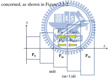
have to be concerned, as shown in Figure 2.2-2.
Figure 2.2-2 a multimode taper is divided into a series of individual waveguides with fixed width. Each section of the individual waveguide can be expressed by a transfer matrix Pm
describing the amplitude variations of the forward and backward propagating modes at two adjacent sections
Here, we introduce the bidirectional mode expansion method for analysis of the
18
are concerned and the field at arbitrary position z in the m-th waveguide can be written as
(
, ,)
( )
,[
exp(
(
)
)
exp(
(
)
)
]
(eq.2.2-14)0
∑
= − + − − = = N i m i m i m i m i m i m x x y z z E x y C i z mdz B i z mdz E β β(
)
( )
,[
exp(
(
)
)
exp(
(
)
)
]
(eq.2.2-15) , , 0 0 mdz z i B mdz z i C y x E w z z y x H m i m i m i m i m i N i m i m x − + − − = =∑
= β β µ βwhere Cim is the modal coefficient for forward wave and Bim is the modal coefficient for
backward wave.
At the interface between the m-th and m+1-th waveguide, the tangential electric and
magnetic fields have to be continuous
(
)
(
, , 1)
(
, ,(
1)
)
(eq.2.2-16) Eym x y z = m+ dz =Emy+1 x y z = m+ dz(
)
(
, , 1)
(
, ,(
1)
)
(eq.2.2-17) Hxm x y z= m+ dz =Hxm+1 x y z= m+ dzBy these two conditions, we obtain a transfer matrix Pm and the modal coefficients can be
calculated by the following relations
18) -2.2 (eq. where 0 0 1 1 = = = + + m N m m m N m m m m m m m B B B C C C B C P B C 、
When a multimode taper is connected to a MMI waveguide, the power is coupled into
several modes of the MMI waveguide. The field propagates at arbitrary position z in the MMI
waveguide is then written as
(
, ,)
[
exp(
(
)
)
exp(
(
)
)
]
( )
, (eq.2.2-19) 0∑
= − + − − = N i M i t i M i t i M i m x x y z C i z L B i z L E x y E β β19 20) -2.2 (eq. 0 0 0 = B C P P P B C m M M M
As the modes propagate through the taper, the propagation constant induces the phase
term and the corresponding modal coefficients CM and BM become complex numbers. We
rewrite the CM and BM by the amplitude term and phase term as eq. 2.2-21 and eq. 2.2-22
(
)
(eq.2.2-21) exp | | CiM = CiM −iθiC(
)
(eq.2.2-22) exp | | BiM = BiM −iθiBBy taking the eq. 2.2-21 and eq. 2.2-22 into eq. 2.2-19, the field at any position is rewritten as
eq. 2.2-23.
(
)
(
)
[
]
(
)
(
[
(
)
]
)
[
exp exp]
( )
, (eq.2.2-23), , 0
∑
= + − + + − − = N i M i B i t i M i C i t i M i m x y x E L z i B L z i C z y x E θ β θ βFrom eq. 2.2-23, we find each mode has an initial phase term, this phase term effects the
distance of the first self-imaging. And the modal coefficient decides the profile of self-image.
Therefore, we can make the self-imaging occurs in a MMI waveguide by multimode taper.
And we can control the property of multimode-interference by changing the structure of
20
Chapter 3 Design approach
In this chapter, we show the design approach to achieve compact waveguide crossing by
integrating multimode tapers to the MMI based waveguide crossings. The output field at the
junction of the MMI waveguide and the multimode taper is coupled into both fundamental
mode and next high order mode of the MMI waveguide, and thus the self-image is formed at
the crossing region to suppress the divergence of the field. Here, we use three dimensional
finite difference time domain (FDTD) method[17] to discuss the effects of taper lengths ad
profiles on the performances of the MMI based waveguide crossing and to find the optimize
design parameters for achieving compact, small loss and low crosstalk waveguide crossings.
3.1 Structure of the designed MMI based waveguide crossing
The structure of our designed MMI based waveguide crossing is displayed in Figure
3.1-1. The device is made on a silicon on insulator substrate where the Silicon (n=3.45) with
thickness of 220 nm is deposited on a SiO2 buffer layer (n=1.45). The input and output
waveguides with width Wg of 500 nm are single-mode. The crossing region is composed of
two 90° intersected MMI waveguides with lengths of Lm and widths Wm of 1200 nm to
support three modes in MMI waveguides. Multimode tapers are used to connect the
input/output and the MMI waveguides. The length of the multimode taper is Lt and its width
is varied from 500 nm to 1200 nm. The length of MMI waveguide Lm is chosen to be twice of
21
22
3.2 Eigenmode properties of the input/output and MMI
waveguides
Figure 3.2-1 shows the cross-section of the designed input waveguide and only the
fundamental TE-like mode is supported in the input and output waveguides at the concerned
wavelength of 1550 nm.
Figure 3.2-1 The cross-section of designed input/output waveguides
By using the Beam Propagation Method (BPM), the fundamental TE-like mode profile
of the input waveguide is calculated and its mode distribution is shown in Figure 3-2. As
shown in Fig 3.2-2, the power of the light is highly confined inside the silicon core. The
23
Figure 3.2-2 The fundamental mode profile of the input and output waveguides.
On the other hand, the width of the MMI waveguide (Wm) is designed to be 1200 nm and
its height (H) is the same as that of the input waveguide, i.e., H is 220nm. In such design,
the MMI waveguide supports three TE-like modes (i.e., TE00, TE01, TE02 modes). We
calculate the mode profiles of these TE-like modes by using BPM method. The calculated
mode profiles of these TE-like modes are shown in order in Figure 3.2-3 ~5. According to
eq. 2-3, an arbitrary field propagating along the MMI waveguide can be linearly combined by
these three TE-like modes.
1) -3.2 (eq. ) , , ( 0 1 2 02 2 01 1 00 0 z i z iβ z iβ CTE e C TE e e TE C z y x E = − + − + −β
Let the field E(x,y,z) be the fundamental mode of the input waveguide. Because the
fundamental mode is centrosymmetric in the x-direction as shown in Figure 3-2, C1 is zero
24
combination of TE00 and TE02 modes, and the self-image is observed as the phase difference
between these two modes becomes 2mπ, m is integer, i.e., the field of the self-image is expressed as
( )
, (eq.3.2-2) Ey x y =C0TE00+C2TE02Based on eq. 2-5, the beat length of the MMI waveguide is calculated as
3) -3.2 (eq. (nm) 2271 2 2 0 = − = β β π B L
25
26
27
28
3.3 Diffraction loss with different self-image profiles
The major loss of a waveguide crossing is the loss at the crossing region because of
vanish of lateral confinement there. We define the loss at the crossing region as diffraction
loss and it can be calculated by
1) -3.3 (eq. -10log loss iffraction D = before after P P
where Pbefore is the power in the MMI waveguide before passing the crossing region and Pafter
is the power in the MMI waveguide after propagating through the crossing region.
The diffraction loss of a MMI based waveguide crossing is reduced because the a focusing self-image is formed at the crossing region. Here, we investigate the effect of the
self-image profile on the diffraction loss by launching the field in the MMI waveguide
constructed by different portion of TE00 and TE02 modes. From eq. 3.2-2, the input field
profile can be decided by the modal coefficients of C0 and C2 , and we define the amplitude
ratio η of C2 to C0 as 2) -3.3 (eq. 0 2 C C = η
The diffraction loss as a function of the amplitude ratio η is shown in Figure 3-3-1. The diffraction loss is about 0.6 dB at the ratio η of zero. As the ratio η increases, the diffraction loss decreases first and then increases as η>0.27. At η=0.27, the lowest diffraction loss is obtained, ~0.12 dB
29
0.0
0.2
0.4
0.6
0.8
1.0
0.0
0.2
0.4
0.6
0.8
1.0
1.2
1.4
1.6
D
iffr
a
cti
o
n
l
o
ss
(d
B
)
Amplitude ratio
η = C2/C0
Figure 3.3-1 Diffraction loss as a function of amplitude ratio η
The corresponding self-image profile at different amplitude ratios are shown in Figure
3.3-2. As η increases from 0 to 0.27, the beam waist of the filed inside the guiding region decrease and the field outside the guiding region also reduces, demonstrating a focusing beam
with narrow angular spectrum is obtained. At η=0.27, the field outside the guiding region is approximately zero with the field profile well fit with a Gaussian function. On the contrary,
as η larger than 0.27, the beam waist inside the guiding region keep reducing but the field outside the guiding region increases, showing the field has more amount of the high-angular
30 -1500 -1000 -500 0 500 1000 1500 0.0 0.2 0.4 0.6 0.8 1.0 1.2 1.4
N
o
rm
a
liz
e
d
e
le
c
tr
ic
f
ie
ld
d
is
tr
ib
u
tio
n
|
E
x
|
x (nm)
-1500 -1000 -500 0 500 1000 1500 0.0 0.2 0.4 0.6 0.8 1.0 1.2 1.4N
o
rm
a
liz
e
d
e
le
c
tr
ic
f
ie
ld
d
is
tr
ib
u
tio
n
|
E
x
|
x (nm)
(a) η = 0.07 (b) η = 0.1831 -1500 -1000 -500 0 500 1000 1500 0.0 0.2 0.4 0.6 0.8 1.0 1.2 1.4
N
o
rm
a
liz
e
d
e
le
c
tr
ic
f
ie
ld
d
is
tr
ib
u
tio
n
|
E
x
|
x (nm)
-1500 -1000 -500 0 500 1000 1500 0.0 0.2 0.4 0.6 0.8 1.0 1.2 1.4N
o
rm
a
liz
e
d
e
le
c
tr
ic
f
ie
ld
d
is
tr
ib
u
tio
n
|
E
x
|
x (nm)
Fig. 3.3-2 Variations of field distributions normalized by the power of the self-image at amplitude ratio η of (a) 0.07, (b) 0.18, (c) 0.27 and (d) 0.51
(d) η = 0.51 (c) η = 0.27
32
3.4 Multimode taper design
Here, we study the effect of the taper length on the self-image profile in the MMI waveguide. As shown in Figure 3.4-1, the taper width varies linearly from Wg to Wm with
its length of Lt and taper height is fixed to be 220 nm. We change Lt from 0 to 2000 nm.
Figure 3.4-2 shows the simulated electric field Ex propagating along the linear taper and the
MMI section with different taper lengths. The lengths of these taper are (a) 0 nm, (b) 500 nm,
(c) 1000 nm, and (d) 2000 nm, respectively. In the absence of the taper ( i.e., Lt is 0 nm.), the
input field is coupled into the two lowest even modes of the MMI waveguide ( TE00、TE02
modes) at the interface between the input and the MMI waveguide and the first self-image is
formed after propagating 2271 nm (i.e. a beat length) in the MMI waveguide as shown in
Figure 3.4-2 (a).
Figure 3.4-1 The diagram of a multimode taper
Lt
Wm
33
In the case of the taper length of 500 nm as shown in 3.4-2 (b), the beam width of the self-image becomes wider and the distance where the first self-image is formed becomes
shorter than a beat length. Base on eq. 3.2-3, the beat length is constant for a given MMI
waveguide. Here, we define the distance where the self-image is formed as the effective beat
length Leff. As the taper length increases, we see that the self-image profile and the effective
beat length are different, and next we study the effect of the length of this linear taper on the
amplitude ratio corresponding to the realized self-image profile, transition loss and the
effective beat length.
34
Figure 3.4-2 Evolution of the input guided mode propagation through the linear taper with its length of (a) 0, (b) 500, (c) 1000 and (d) 2000 nm and the MMI
waveguide (a) Lt = 0 nm
(b) Lt = 500 nm
(c) Lt = 1000 nm
35
3.4.1 Effect of taper length on the amplitude ratio
η
As shown in Figure 3.4-2, the field distribution along the MMI waveguide is different as
the taper length changes and we use overlap integral to acquire the modal coefficients of TE00
and TE02 modes for all cases of the different taper lengths. The variation of the taper length
on amplitude ratio is shown in Figure 3.4-3.
0 500 1000 1500 2000 0.0 0.1 0.2 0.3 0.4 0.5
A
m
pl
it
ude
r
a
ti
o
η
Taper length (nm)
Figure 3.4-3 Variation of taper length on the amplitude ratio
As Lt=0 nm, 20.11% of the input field is coupled into the TE02 mode and the
corresponding amplitude ratio is 0.51. As the taper length Lt increases, the power coupled into
the TE02 mode decreases and thus the amplitude ratio η reduces monotonically. In section
3.3, we obtained the lowest diffraction loss as η=0.27. To achieve this condition, the length of this linear taper has to be 560 nm.
36
3.4.2 Effect of taper length on transition loss
Conventionally the taper is inserted in between two mismatched waveguides in order to
reduce the transition loss. Here, we study the effect of taper length on the transition loss and
the results are shown in Figure 3.4-4. As the taper length is zero, some input power is
radiated and reflected at the interface of the input and MMI waveguides due to mode
mismatch. By using overlap integral, the transition loss is calculated to be 0.226 dB,
corresponding to the total coupling efficiency of 94.93%. As shown in Figure 3.4-4, the
transition loss decreases with the increase of the taper length. In addition, the reduction of the
transition loss is steep as the taper length increases from 0 to 1000 nm. The transition loss is
smaller than 0.003 dB ( i.e., the coupling efficiency is more than 99.93% ) as the taper length
is larger than 1000 nm. As the taper length is 560 nm, the transition loss is roughly equal to
37 0 500 1000 1500 2000 0.00 0.05 0.10 0.15 0.20 0.25 T ra ns it io n lo ss ( dB ) Taper length L t (nm)
38
3.4.3 Effect of taper length on the effective beat length
We notice that Leff are varied with the taper length in Figure 3.4-2. The variations of the
effective beat length Leff with the taper length Lt is displayed in Figure 3.4-5. Without
inserting a taper (i.e., Lt=0 nm), the effective beat length is equal to the beat length. As the
taper length Lt increases, the effective beat length Leff decreases and is smaller than the beat
length. 0 500 1000 1500 1600 1700 1800 1900 2000 2100 2200 2300
E
ffe
cti
v
e b
ea
t l
en
g
th
(n
m
)
Taper length (nm)
Figure 3.4-5 Effective beat length Leff as a function of the taper length Lt.
When the field propagates through this multimode taper, a phase difference between
TE00 and TE02 modes is induced at the junction of the multimode taper and the MMI
waveguide because the modes interfere along this multimode taper. The self-image with phase
difference of 2π is observed as the field propagates an effective beat length along the MMI waveguide. The effective beat length, therefore, can be calculated by
1) -3.4 (eq. difference phase initial 2 2 0 β β π − − = eff L
39 of the multimode taper.
As the taper length increases, the length for mode interference increases. As a result,
the initial phase difference increases and the effective beat length decreases with the increase
of the taper length. As the taper length is 560 nm, the corresponding effective beat length is
1889.3 nm and the length of MMI waveguide is chosen to be twice of the effective beat length
40
3.5 Performances of MMI based crossings with linear tapers
Figure 3.5-1 shows the FDTD simulation results of these taper-integrated MMI based waveguide crossings with the taper length Lt of 0 nm, 560 nm, 1000 nm and 2000 nm,respectively. Here, the length of the MMI section in each design is chosen to be twice of the
effective beat length obtained in the aforementioned section. In the case of Lt = 0 nm, field
is diffracted dramatically at the crossing region and significant scattering field radiates into
the orthogonal MMI waveguide. In the case of Lt = 560 nm, we see a narrowing field at the
center of the crossing and the wave fronts at the front and back of the crossing are almost the
same with reversal sign of phases. In the cases of the larger Lt, as shown in Figure 3.5-1 (c)
and (d), the field scatters through the crossing region without significant crosstalk because the
dominant component of the field is the TE00 mode with a narrow angular spectrum.
However, we can see wave front expands more widely at the back of the crossing region, and
this results in more insertion loss.
Table 1 lists the parameters and performance of these four taper-integrated MMI
crossing structures with taper lengths of 0, 560, 1000 and 2000 nm, respectively. As η decreases, dimension of the crossing increases but the crosstalk decreases. The lowest
insertion loss of these taper-integrated MMI based crossings is obtained as the taper length is
41
In the case of Lt = 0 nm, the diffraction loss is roughly equal to 0.58 dB and the insertion
loss (~0.78 dB) is roughly equal to the sum of the transition loss (0.226 dB) and diffraction
loss, meaning 16.44% of the input power is lost after the filed propagates through the MMI
based waveguide crossing without inserting a taper. In the case of Lt=560 nm (for η = 0.27),
the diffraction loss is about 0.12 dB and its insertion loss is 0.24 dB.
In the cases of Lt = 1000 nm and 2000 nm, the field diverges at the crossing region such
that the guided modes of the MMI waveguide and the diverged field at the back of the
crossing are mismatch, resulting in substantial insertion loss. Compared with the MMI based
crossing without inserting tapers (i.e. the case of Lt = 0), the taper-integrated MMI based
42
Figure 3.5-1 FDTD simulations of the input guided mode propagation through MMI based waveguide crossings sandwiched by four identical linear tapers
with (a) Lt=0 and Lm=4543.4 nm, (b) Lt=560 nm and Lm=3778.5 nm, (c)
Lt=1000 nm and Lm=3600 nm and (d) Lt=2000 nm and Lm=3450.4 nm.
Table 1 Properties of MMI based waveguide crossings integrated with linear tapers at the wavelength of 1550 nm L t (nm) η Leff (nm) L m+2Lt (nm) Insertion loss (dB) Crosstalk (dB) 0 0.52 2271.7 4543.4 0.78 -23.19 560 0.27 1889.3 4898.5 0.24 -45.39 1000 0.18 1800.0 5600.0 0.25 -48.12 2000 0.07 1725.2 7450.4 0.43 -50.63 (a) (b) (c) (d)
43
3.6 Effect of the Taper Profiles
In the previous section, we realized the smallest insertion loss as the amplitude ratio η = 0.27. In order to achieve this value, the corresponding linear taper length Lt is 560 nm, and,
as a consequence, the transition loss of this taper is 0.08dB and the effective beat length is
1889.3 nm.
Here, we investigate the effect of the taper profiles on the transition loss and the effective
beat length. The studied taper profiles expand in width with an initial value of 500 nm to the
final value of 1200 nm and are given by
( )
(
)
(eq.3.6-1) n t g m g t L z w w w z w × − + =where wt(z) is the taper width and n is the profile index .
Here, we chose the taper profiles with n = 0.25, 0.5, 1 and 2 and the corresponding Lt are 750,
530, 560 and 1000 nm in order to realize η=0.27.
The field distributions along these four taper and MMI sections are shown in Figure
3.6-1. In the case of n=0.25 and n=0.5, the width varies steeply, and, as a result, the
effective beat length for each design decreases to be 1400 nm and 1735 nm, respectively.
However, the transition loss is larger than the case of the linear taper. In the case of n=2, the
44
Figure 3.6-1 Evolution of the input guided mode propagation through different taper profiles with n= (a) 0.25, (b) 0.5, (c) 1 and (d) 2 and the MMI waveguide
(a) Lt = 750 nm, n=0.25
(b) Lt = 530 nm, n=0.5
(c) Lt = 560 nm, n=1
45
Figure 3.6-2 FDTD simulations of the input guided mode propagation through MMI based waveguide crossings sandwiched by four different tapers with (a) Lt=750nm and n=0.25, (b) Lt=530 nm and n=0.5, (c) Lt=560 nm and n=1 and
(d) Lt=1000 nm and n=2.
Table 2 Performance of waveguide crossings with different taper profiles at the wavelength of 1550 nm n Lt (nm) Leff (nm)
Total length of the crossing Lm+2Lt (nm) Transition loss (dB) Insertion loss (dB) Crosstalk (dB) 0.25 750 1400.0 4300.0 0.17 0.37 -39.83 0.5 530 1735.0 4530.0 0.12 0.33 -42.85 1 560 1889.3 4898.5 0.08 0.24 -45.39 2 1000 1900.0 5800.0 0.02 0.15 -42.34 (a) (b) (c) (d)
46
Figure 3.6-2 exhibits the simulated fields of the input wave propagating through these
taper-integrated MMI based crossings with (a) n=0.25, (b) n=0.5, (c) n=1 and (d) n=2. The
transverse fields at the junction of the taper and the input waveguide are different but the
self-images formed at Leff of the MMI waveguide in these cases have the same beam waist at
due to the fixed value of η.
Table 2 summarizes the parameters and performances of simulated taper-integrated MMI
based crossings at the wavelength of 1550 nm for the cases of n = 0.25, 0.5, 1 and 2. The
lengths of the MMI crossings in the cases of n = 0.25 and n=0.5 are less than twice of the beat
length and their insertion loss are lower than that without inserting a taper. Although the
dimension of the MMI crossing increases as n increases, the transition loss of the taper
decreases and better performance of the waveguide crossing is obtained. In the case of n = 2,
the MMI waveguide crossing has the insertion loss of 0.15 dB and the dimension of 5800×
47
3.7 Wavelength dependence on insertion loss and crosstalk
Insertion losses and crosstalks of these designed MMI based waveguide crossings with
different taper profiles as a function of wavelength are shown in Figure 3.7 (a) and (b). The
insertion loss decreases as n increases because the transition losses of the tapers reduce. In
each case, the variations of insertion loss is less than 0.1 dB at the wavelength ranging from
1500 to 1600 nm. All the crosstalks of these MMI based crossings are lower than -30 dB at
the wavelength ranging from 1500 to 1600 nm. These results indicate these crossings exhibit
broad transmission spectra around the wavelength of 1550 nm. In the case of n = 2, the
insertion loss is averagely 0.18 dB and the crosstalk is less than -40 dB.
Figure 3.7 (a) Simulated insertion loss spectra and (b) calculated crosstalk spectra of the designed MMI-based waveguide crossings for n=0.25 (black
curves), 0.5 (red curves), 1 (blue curves) and 2 (green curves)
(a) (b) 1500 1520 1540 1560 1580 1600 -50 -45 -40 -35 -30 C ro ss ta lk ( dB ) Wavelength (nm) n=0.25 n=0.5 n=1 n=2 1500 1520 1540 1560 1580 1600 0.0 0.1 0.2 0.3 0.4 0.5 In se rt io n l o ss ( d B ) Wavelength (nm) n=0.25 n=0.5 n=1 n=2
48
Chapter 4 Conclusion
In this thesis, we present a novel compact MMI based crossing by using multimode
tapers. As a short multimode taper is inserted in between the input/output and MMI
waveguides, the transition loss reduces and the length of the required multimode waveguide
reduces to be less than twice of the beat length. Besides, the diffraction loss is determined by
the profile of the self-image, and its minimum is obtained as η is 0.27.
In the case of using the quadratic taper, the size of the MMI based waveguide crossing is
5800×5800 nm2, the insertion loss is around 0.15 dB and the crosstalk is lower than -40 dB. In
49
References
[1] P. Koonath, et al., "Monolithic 3-D silicon photonics," Journal of Lightwave
Technology, vol. 24, pp. 1796-1804, Apr 2006.
[2] B. Jalali, "Can silicon change photonics?," Physica Status Solidi a-Applications and
Materials Science, vol. 205, pp. 213-224, Feb 2008.
[3] A. S. Liu, et al., "200 Gbps Photonic Integrated Chip on Silicon Platform," in 5th
IEEE International Conference on Group IV Photonics, Sorrento, ITALY, 2008, pp.
368-370.
[4] B. Jalali, et al., "Advances in silicon-on-insulator optoelectronics," Ieee Journal of
Selected Topics in Quantum Electronics, vol. 4, pp. 938-947, Nov-Dec 1998.
[5] A. G. Rickman, et al., "SILICON-ON-INSULATOR OPTICAL RIB WAVE-GUIDE
LOSS AND MODE CHARACTERISTICS," Journal of Lightwave Technology, vol. 12, pp. 1771-1776, Oct 1994.
[6] L. Liao, et al., "High speed silicon Mach-Zehnder modulator," Optics Express, vol. 13, pp. 3129-3135, Apr 2005.
[7] Y. M. Kang, et al., "Monolithic germanium/silicon avalanche photodiodes with 340 GHz gain-bandwidth product," Nature Photonics, vol. 3, pp. 59-63, Jan 2009.
[8] H. S. Rong, et al., "An all-silicon Raman laser," Nature, vol. 433, pp. 292-294, Jan 2005.
[9] H. S. Rong, et al., "A continuous-wave Raman silicon laser," Nature, vol. 433, pp. 725-728, Feb 2005.
[10] T. Fukazawa, et al., "Low loss intersection of Si photonic wire waveguides," Japanese
Journal of Applied Physics Part 1-Regular Papers Short Notes & Review Papers, vol.
43, pp. 646-647, Feb 2004.
[11] W. Bogaerts, et al., "Low-loss, low-cross-talk crossings for silicon-on-insulator nanophotonic waveguides," Optics Letters, vol. 32, pp. 2801-2803, Oct 2007.
[12] P. Sanchis, et al., "Highly efficient crossing structure for silicon-on-insulator waveguides," Optics Letters, vol. 34, pp. 2760-2762, Sep 2009.
[13] W. Q. Ding, et al., "Compact and low crosstalk waveguide crossing using impedance matched metamaterial," Applied Physics Letters, vol. 96, Mar 2010.
[14] H. L. Liu, et al., "Low-loss waveguide crossing using a multimode interference structure," Optics Communications, vol. 241, pp. 99-104, Nov 2004.
[15] H. Chen and A. W. Poon, "Low-loss multimode-interference-based crossings for silicon wire waveguides," Ieee Photonics Technology Letters, vol. 18, pp. 2260-2262, Nov-Dec 2006.
50
[16] L. B. Soldano and E. C. M. Pennings, "OPTICAL MULTIMODE INTERFERENCE
DEVICES BASED ON SELF-IMAGING - PRINCIPLES AND APPLICATIONS,"
Journal of Lightwave Technology, vol. 13, pp. 615-627, Apr 1995.
[17] K. S. Yee and J. S. Chen, "The finite-difference time-domain (FDTD) and the finite-volume time-domain (FVTD) methods in solving Maxwell's equations," Ieee