D. Y. Lin , J. J. Shiu, J. D. Wu, C. S. Yang, and W. C. Chou
1 Department of Electronic Engineering, National Changhua University of Education Changhua,
Taiwan, R.O.C
2 Department of Electrophysics, National Chiao Tung University Hsinchu, Taiwan, R.O.C
Received 4 September 2006, revised 22 December 2006, accepted 22 December 2006 Published online 11 April 2007
PACS 78.55.Cr, 78.67.De
The optical characterization of type II Zn0.97Mn0.03Se/ZnSe0.92Te0.08 multiple-quantum-well structures have been studied using photoluminescence (PL), temperature-dependent PL, polarized PL, power-dependent PL, and photoreflectance (PR) in this study. The PL data reveal that the band alignment of the ZnMnSe/ ZnSeTe system is type II. Comparing with the theoretical calculation based on the Schrodinger equation, the valence band offset is estimated to be 0.6 eV. From the power-dependent PL spectra, it is observed that the peak position of PL spectra shows a blueshift under different excitation power. The blueshift can be interpreted in terms of the band-bending effect due to spatially photoexcited carriers in a type II alignment. The thermal activation energy (EA) for quenching the PL intensity was determined from tem- perature-dependent PL spectra. The thermal activation energy was found to decrease as the thickness of ZnMnSe and ZnSeTe layers decreased. The polarized PL spectra exhibit a large in-plane polarization with the polarization degree up to 50%. The polarization does not depend on the excitation intensity as well as temperature. The large polarization is an inherent orientation of the interface chemical bonds.The higher transition features observed in PR spectra show a blueshift with the similar trend observed in the PL spec-tra as decreasing the thickness of ZnSeTe layer. This result provides a consistent evidence for the assump-tion that square-like well shapes were built in the ZnSeTe layers.
© 2007 WILEY-VCH Verlag GmbH & Co. KGaA, Weinheim
1 Introduction
Wide-gap II – VI semiconductor materials have been successfully applied in a variety of optoelectronic devices, e.g., photodetectors and light sources for the UV, blue and green spectral regions [1, 2]. In re-cent years the incorporation of diluted-magnetic-semiconductor (DMS) layers in quantum-well structures has attracted a lot of attention due to its potential applications in quantum computation, as well as its interesting physical properties of building materials. A spin injector, or spin aligners, consisting of II –VI compound DMS heterostructures, as well as III – V compound semiconductor heterostructures have been fabricated [3, 4]. In order to improve the performance of the devices or develop new applications, we need to have a comprehensive understanding of the physical properties of the building materials. The ZnMnSe layer has been served as a spin carrier selection valve in spin-LED [5]. The ZnSeTe layer is a strong iso-electronic hole-trapping material, which can be used as a memory storage site with a size of less than 1 nm [6]. In this work, we present the interesting optical properties of ZnMnSe/ZnSeTe multi-ple-quantum-wells (MQWs). From the PL spectra, we found that the band alignment of the ZnMnSe/ ZnSeTe system is type II. Comparing with the theoretical calculation based on the Schrödinger equation,
phys. stat. sol. (b) 244, No. 5 (2007) 1645 Paper
the valence band offset can be estimated. The thermal activation energy was determined from the tem-perature-dependent PL spectra. The activation energy with the different thickness of ZnMnSe or ZnSeTe layers was also investigated. A large in-plane polarization is observed in polarized PL measurements. It is attributed to an inherent orientation of the interface chemical bands. The excitation power-dependent PL results reveal a giant blueshift of the peak energy. It can be explained in terms of the band-bending effect due to the spatially separated photoexcited carriers in a type II bandgap alignment. For PR spectra the optical features corresponding to the ground and excited state transitions were found and discussed.
2 Experimental
The Zn1–xMnxSe/ZnSe1–yTe MQWs studied in this work were grown on GaAs substrates by molecular beam epitaxy (MBE) system and consisted of the following layers, listed in order from substrate to sur-face: a ZnSe buffer layer (220 nm), a 10 period stack of Zn0.97Mn0.03Se/ZnSe0.92Te0.08 MQWs. For the first set of samples, the thickness of the ZnSeTe (W1) layers is fixed at 20 nm while the thickness of ZnMnSe (W2) layers is varied among 5, 3, and 1 nm, respectively. These three samples were recognized as sample A, B, and C, respectively. For the second set of samples, the thickness of the ZnMnSe layers is fixed at 20 nm while the thickness of ZnSeTe layers is varied among 5, 3, and 1 nm, respectively. These three samples were recognized as sample D, E, and F, respectively. For PL measurements, the sample was excited by a He – Cd laser (325 nm, 18 mW). the spectra were dispersed by a PTI 0.25 m monochroma-tor, and detected by a photomultiplier tube (PMT). For polarized PL measurement, a linear polarizer has been placed in front of the monochromator to record the PL signal polarized at different polarization angles. A closed cycle helium refrigerator equipped with a heater and a temperature controller to control the temperatures varying in the range between 15 and 300 K. The PR measurements were performed using a 150 W Xeon lamp filtered by a PTI 0.25 m monochromator to provide the monochromatic light which is chopped at 200 Hz. A He – Cd laser, chopped at 250 Hz, was employed to provide the modulat-ing source. The laser light intensity was reduced to about 5 – 10% of its initial value by usmodulat-ing a neutral density filter. The laser beam overlaps the monochromatic probe beam on a spot of the sample surface. The reflected light was detected by a PMT and the signal was recorded by a lock-in amplifier with a reference signal working at frequency of 450 Hz to diminish the effect of scattering light.
3 Results and discussion
Figure 1 shows PL spectra of the first set of samples taken at 15 K. A small blueshift of 54 meV was found as the thickness of ZnMnSe layer decreases from 5 nm to 1 nm. Figure 2 shows PL spectra of the second set of samples taken at 15 K. A larger blueshift of 198 meV was observed when the thickness of
1.8 1.9 2.0 2.1 2.2 2.3 2.4 ↑↑↑↑ ↑↑↑↑ ↑↑↑↑ @ 15 K 2.124 eV 2.072 eV 2.07 eV Sample C (W2= 1 nm) Sample B (W2= 3 nm) Sample A (W2= 5 nm) P L In tens it y (a. u. )
Photon Energy (eV)
1.6 1.8 2.0 2.2 2.4 2.6 ↑↑↑↑ ↑↑↑↑ ↑↑↑↑ x15 @ 15 K 2.282 eV 2.14 eV 2.084 eV Sample F (W1= 1 nm) Sample D (W1= 5 nm) Sample E (W1= 3 nm) P L In tens it y (a. u. )
Photon Energy (eV)
0 1 2 3 4 5 6 -0.02 0.00 0.02 0.04 0.06 0.08 Bl ue sh if ZnSe 0.92Te0.08thickness (nm) 1.85 1.90 1.95 2.00 2.05 2.10 2.15 2.20 2.25 (110) P L In tens
Photon Energy (eV)
ZnSeTe layer reduces from 5 nm to 1 nm. Both in Figs. 1 and 2, the spectra are displaced vertically for clarity. The bandgap of ZnMnSe and ZnSeTe is near 2.8 and 2.7 eV at 15 K, respectively. It is observed that the PL peak energy is much smaller than the bandgaps of composing materials. This result con-firmed that the band alignment of the ZnMnSe/ZnSeTe system is type II. In ZnMnSe/ZnSeTe MQWs, electrons are confined in the ZnMnSe layers and holes are localized in the ZnSeTe layers. The PL signal is generated from the recombination of the accumulated electrons and holes near the interface. So the emission peak located at the photon energy smaller than the bandgaps of ZnMnSe and ZnSeTe.
For samples A, B, and C, as the thickness of ZnMnSe layer decreases from 5 to 1 nm, only a small blueshift of 54 meV is observed. This value is much lower than the calculated data based on a square well assumption. For samples D, E, and F, the thickness of ZnMnSe layer is fixed at 20 nm. Figure 3 presents the blueshift of experimental data (solid squares) and theoretical calculation results (solid cur-ves) versus hole-well width at different offset values, in which the experimental and theoretical values of sample D were used as reference for calculating the blueshift. The change in quantized fundamental energy level, calculated by assuming a square ZnMnSe well, matches measured blueshift by setting the valence band offset as 600 meV and the effective mass of holes as 0.6m0.
Figure 4 shows the PL spectra of sample A for the emitted radiation polarized along ·110Ò and ·1 10Ò direction. In type-II QW structures the spatially indirect transitions, which arise from the electron – hole wave function overlap within an extremely narrow region adjacent to the interface, contain information about interface properties. The polarization direction is related to the interface bond directions in different interfaces [7]. The interfaces in ZnMnSe/ZnSeTe heterostructure mainly consist of Zn – Se and Se – Zn bonds. If we take the growing direction as z-axis and assume the bond direction of Zn–Se is parallel to axis ·110Ò, then the bond direction of Se – Zn would be parallel to axis ·1 10Ò. The chemically different bonds are located on different atomic planes.
The normalized PL peak intensity versus the angles of the analyzer for sample A is presented in the inset of Fig. 4. Open squares are experimental data and the curves are the fits to cos .2θ The polarization degree was defined as
110 110 110 110 l I I P I I -Ê ˆ = ÁË + ˜¯ . (1)
In this study we observed that the polarization degree obtained from the samples of set two (40 to 60%) is larger than that in the samples of set one (25 to 35%). It may due to a larger built-in electric field re-sulting from a larger strain in ZnSe buffer layer which is observed by modulation spectroscopy.
Fig. 3 (online colour at: www.pss-b.com) Calculated blueshift of optical transition energies (lines) and ex-perimental data (solid squares) versus the thickness of the ZnSeTe layer.
Fig. 4 Polarized PL spectra of ZnMnSe/ZnSeTe MQWs at 15 K.
phys. stat. sol. (b) 244, No. 5 (2007) 1647 Paper 1.9 2.0 2.1 2.2 2.3 ↑ ↑↑ ↑ ↑ ↑↑ ↑ ↑ ↑↑ ↑ ↑ ↑↑ ↑ ↑ ↑↑ ↑ ↑ ↑↑ ↑ ↑ ↑↑ ↑ ↑ ↑↑ ↑ ↑ ↑↑ ↑ ↑ ↑↑ ↑ ↑ ↑↑ ↑ ↑ ↑↑ ↑ ↑ ↑↑ ↑ Sample B x38 x22 x11 x6 x4 x2.5 x1.5 70 K 60 K 50 K 40 K 30 K 20 K 65 K 55 K 45 K 35 K 25 K 12 K 15 K P L In tens it y (a. u. )
Photon Energy (eV)
1 2 3 4 5 5 10 15 20 Sample A, B, C Sample D, E, F Ac ti v a ti o n en er g y (me V)
Layer thickness of ZnMnSe or ZnSeTe (nm)
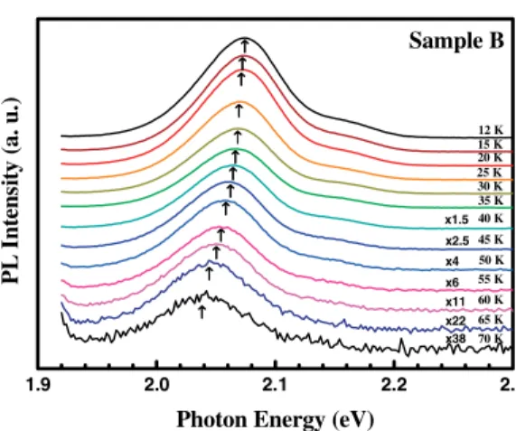
The temperature-dependent PL spectra taken from sample B are presented in Fig. 5 as an example. As the temperature increases, the PL intensity drops rapidly and the transition peaks show a redshift, which is due to the decrease in the bandgap energy. The temperature-dependence of the integrated PL intensity (IPL) could be expressed as
( )
0 PL A B 1 exp I I T E A k T = -Ê ˆ + ÁË ˜¯ , (2)where T is the temperature, kB is the Boltzmann contant, I0 is the integrated PL intensity near 0 K, A is a constant, and EA is the thermal activation energy. EA is responsible for the quenching of PL intensity in the temperature-dependent spectra. The measured values of integrated PL intensity are fitted using Eq. (2), and then the theoretical curve consists with the experimental data. Therefore, the thermal activa-tion energy EA of the MQW structures can be obtained. The temperature-dependent PL spectra of the other samples have also been performed and similar optical characteristics have been found. Figure 6 summarizes the obtained thermal activation energy of sample A – F versus the thickness of the ZnMnSe or ZnSeTe layer. The thermal activation energy obtained by this method is usually considered as the total binding energy, which includes the confinement energy of electrons or holes and the exciton binding energy. We found that reducing the thickness of ZnMnSe or ZnSeTe layers makes EA to decrease. The temperature-induced quenching of luminescence in the MQW structures proceeds mainly from thermal emission of charge carriers out of confined quantum-well states into barrier states [8]. The subband energies of electron- or hole-well are increased for samples with smaller ZnMnSe or ZnSeTe well thick-ness. Therefore the reduced delocalization energy facilitates the escape of the electrons or holes from the well.
Figure 7 presents the PL spectra of sample C under different excitation intensities at 15 K. A giant blueshift under the different excitation intensities was observed. The PL peak shows a shift of about 17 meV when the pumping intensity increases from 0.37 to 5 mW. In type II heterostructures, the elec-trons and holes are confined in different layers. This giant blueshift can be attributed to the band-bending effect. The band-bending effect is caused by spatially separated potoexcited carriers, in which electrons are confined in the ZnMnSe layer and holes are confined in the ZnSeTe layer. The separated electrons and holes introduce an electric field and cause the bending of the energy band, and then change the over-lapping of the electron and hole wave functions. The photoluminescence is generated from the recombi-nation of the accumulated electrons and holes near the interface. When the power increases, the band-
Fig. 5 (online colour at: www.pss-b.com) PL spectra of sample B under different excitation intensities at 15 K.
Fig. 6 Variation of thermal activation energy with thickness of ZnMnSe or ZnSeTe layer.
1.9 2.0 2.1 2.2 2.3 ↑ ↑↑ ↑ ↑ ↑↑ ↑ ↑ ↑↑ ↑ ↑ ↑↑ ↑ ↑ ↑↑ ↑ x5 x3 x3 x3 x3 PL In te n si
Photon Energy (eV)
0.6 0.8 1.0 1.2 1.4 1.6 1.8 2.120 2.122 2.124 2.126 2.128 2.130 PL P e ak Pos (Power)1/3(mW)1/3
bending effect becomes more pronounced. The accumulated electrons and holes will be confined in a narrower region near the interface. An increase in the excitation density raises the level of the confining potential, and the electron quantization energy is elevated and the blueshift occurs. The electron quanti-zation energy is thus expected to increase proportionally with the third root of the excitation density [9]. Figure 8 shows the relation between the PL peak position and the third root of the excitation energy power. For samples of the same hole well thickness, sample D, E, and F, the blueshift of the PL peak is about 8 meV. Their wide electron well (20 nm) leads to weak built-in electric field accounts for the small blueshift. On the other hand, for sample A, B, and C the blueshift are 10, 11, and 17 meV, respectively. When the thickness of ZnMnSe layer decreases, the band-bending effect is more pronounced and leads to a larger blueshift.
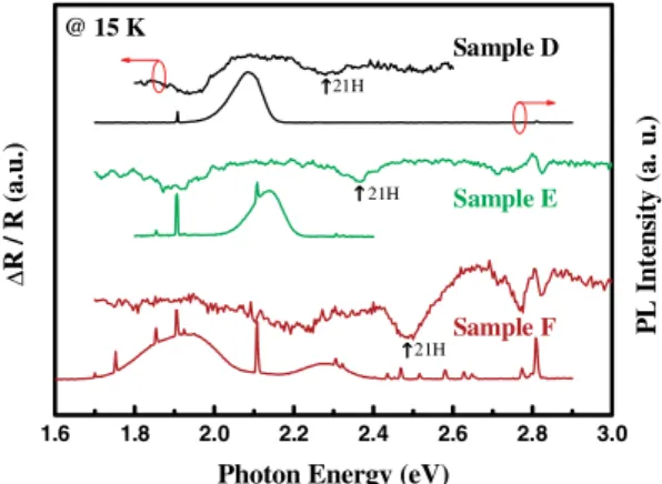
Figures 9 and 10 present the PR spectra and the corresponding PL spectra of the sample A, B, C; and sample D, E, F, respectively. For sample B and C, broadened PR features occur at energies correspond-ing to PL peaks. The key mechanism of PR measurement is absorption modulation, so the broadened PR features of sample B and C reveal the information of absorption transitions. In addition, the PL peaks originate from the recombination of the accumulated electrons and holes near the interface. Based on this fact that both PR and PL spectra show transition features at the same energies, we can understand that
1.6 1.8 2.0 2.2 2.4 2.6 2.8 3.0 Sample C Sample B @ 15 K Sample A P L In tens it y (a . u. ) ∆ R/ R (a .u .)
Photon Energy (eV)
1.6 1.8 2.0 2.2 2.4 2.6 2.8 3.0 ↑ ↑↑ ↑ ↑ ↑↑ ↑ ↑ ↑↑ ↑21H 21H 21H Sample F Sample E Sample D @ 15 K P L Int ensi ty (a. u. ) ∆ R/ R (a .u .)
Photon Energy (eV)
Fig. 7 (online colour at: www.pss-b.com) PL spec-tra of sample C under different excitation intensities at 15 K.
Fig. 8 Dependence of PL peak energy on the cubic root of excitation power.
Fig. 9 (online colour at: www.pss-b.com) PL and PR spectra of the first set samples at 15 K.
Fig. 10 (online colour at: www.pss-b.com) PR and PL spectra of the second set samples at 15 K.
phys. stat. sol. (b) 244, No. 5 (2007) 1649 Paper
the potential well in conduction band is partially filled with electrons. Moreover, the PL spectrum of sample A does not show an absorption bump at the peak energy of PL spectrum but presents another absorption lobe at higher energy. We propose that the lower quantized state in the electron well is fully filled and no absorption transition is allowed. A higher energy state is not filled with electrons, so the absorption lobe at higher energy is revealed. The similar higher transition energies are observed in the PR spectra of sample D, E and F, which are composed of wide (20 nm) electron wells. These spectral features show a blueshift with the similar trend observed in PL spectra as decreasing the thickness of ZnSeTe layer. It is attributed to the transition coming from the quantized state in the hole well to the higher quantized state in the electron well. In Fig. 10 the optical feature locates around 1.9 eV could be assigned as an optical transition related to defect states.
4 Conclusions
We have performed the optical characterization of ZnMnSe/ZnSeTe MQW structures grown by molecu-lar-beam epitaxy using PL, excitation power- and temperature-dependent PL, polarized PL and PR meas-urements. From PL measurements, we confirmed that the band alignment of the ZnMnSe/ZnSeTe system is type II. We also determined the valence band offset is about 600 meV by matching the theoretical calculation with the experimental data. In the temperature-dependent PL spectra, the thermal activation energy was determined. The activation energy tended to decrease as the thickness of ZnMnSe and ZnSeTe layers decreased. From the polarized PL measurements, we found that the PL spectra exhibit a large in-plane polarization at the different angles of polarization. This large polarization is an inherent orientation of the interface chemical bonds. From the power-dependent PL spectra, a large blueshift is found and can be explained by electron band-bending effect in a type II alignment. For PR measure-ments, the higher transitions were observed and supported that the lower quantized electron levels are filled.
Acknowledgements The author acknowledges the support of the National Science Council of the Republic of China under Project No. NSC 94-2112-M-018-003.
References
[1] W. Xie, D. C. Grillo, R. L. Gunshor, M. Kobayashi, H. Jeon, J. Ding, A. V. Nurmikko, G. C. Hua, and N. Otsu-ka, Appl. Phys. Lett. 60, 1999 (1992).
[2] R. L. Gunshor and A. V. Nurmikko, Proc. IEEE 82, 1503 (1994). [3] J. K. Furdyna, J. Appl. Phys. 64, R29 (1988).
[4] N. Dai, H. Luo, F. C. Zhang, N. Samarth, M. Dobrowolska, and J. K. Furdyna, Phys. Rev. Lett. 67, 3824 (1991). [5] B. T. Jonker, Y. D. Park, B. R. Bennett, H. D. C Cheong, G. Kioseoglou, and A. Petou, Phys. Rev. B 62, 8180
(2000).
[6] G. A. Prinz, Science 282, 1660 (1998).
[7] A. V. Platonov, V. P. Kochereshko, E. L. Ivchenko, G. V. Mikhailov, D. R. Yakovlev, M. Keim, W. Ossau, A. Waag, and G. Landwehr, Phys. Rev. Lett. 83, 3546 (1999).
[8] Y. T. Shih, Y. L. Tsai, C. T. Yuan, C. Y. Chen, C. S. Yang, and W. C. Chou, J. Appl. Phys. 96, 7267 (2004). [9] Y. S. Chiu, M. H. Ya, W. S. Su, and Y. F. Chen, J. Appl. Phys. 92, 5810 (2002).