Low efficiency droop of InGaN/GaN blue LEDs with super-lattice
active structure
Shih-Pang Chang
1, Kuok-Pan Sou
1, Jet-Rung Chang
2, Yuh-Jen Cheng
1,3, Yuh-Jing Li
2, Yi-Chen
Chen
1, Hao-Chung Kuo
1, Ken-Yuh Hsu
1and Chun-Yen Chang
21
Department of Photonics & Inst. of Electro-Optical Engineering, National Chiao Tung University,
1001 Ta Hsueh Rd., Hsinchu 300, Taiwan
2
Department of Electronic Engineering, National Chiao Tung University, 1001 Ta Hsueh Rd.,
Hsinchu 300, Taiwan
3
Research Center for Applied Sciences, Academia Sinica, Taipei 11529, Taiwan
ABSTRACT
We report the efficiency droop behaviors of InGaN/GaN blue LEDs with different thickness of GaN quantum barriers (QBs). The droop percentage from efficiency peak to 70 A/cm2 is only about 10% as reducing the thickness of GaN QBs
from 104 Å to 33 Å. A less carrier localization has been observed from wavelength dependent time resoled photoluminescence measurement as reducing the thickness of GaN QBs. The alleviation of droop percentage may due to more uniform distribution of electron and hole carrier in the active region, which resulted from super-lattice (SL) like active structure. The crystalline quality does not become worse from the results of v-pits density even thickness of GaN QBs is as low as 33 Å. The SL like active structure could be a potential structure to alleviate the efficiency droop for the application of solid state general lighting.
Keywords: LEDs, efficiency droop, super-lattice
1. INTRODUCTION
Nitride-based light emitting diodes (LEDs) suffer from the reduction in efficiency at high injection current levels, which is so called efficiency droop [1]. It is imperative to overcome this problem to allow LEDs to produce high luminous flux with reasonably high efficiencies under high current densities operation for use in general lighting. Over the past year, several different mechanisms for the efficiency droop have been suggested; including carrier leakage from the active region [2], nonuniform distribution of holes [3-4], Auger recombination [5-7], and carrier delocalization under high injection carrier density [8-9] are currently considered to be the most likely reasons. In this work, we investigate the efficiency behaviors of InGaN/GaN blue LEDs with different thickness of GaN quantum barriers (QBs).
2. EXPERIMENT
The samples were grown on c-plane (0001) sapphire substrates by metalorganic chemical vapor deposition. A 20-nm-thick AlN nucleation layer was deposited on the sapphire substrate first, and followed by 2 μm undoped GaN and 2 μm Si-doped 5x10-19cm−3 n-type GaN. The four pairs of In
0.06Ga0.94N layer (0.9 nm) and GaN layer (1.2 nm) super-lattices
were used as the pre-strain layer. The multiple-quantum-wells (MQWs) consisted of twelve pairs of GaN barrier (12.5 nm) and In0.15Ga0.85N well 3 nm at 970℃ and 820℃ respectively, the previous six pairs with intentionally Si-doped
n-type 1x10-17cm−3 at the GaN barriers. Finally, a 20-nm electron blocking layer with Mg-doped p-type Al
0.15Ga0.85N and a
200-nm Mg-doped p-type GaN layer with a rough surface morphology for better light extraction. After growth, the LED chips were fabricated by regular chip process with indium tin oxide current spreading layer and Cr/Pt/Au contact metal, and the size of mesa is 254 x 577 μm2. The LED structures with thickness of GaN QBs about 104Å, 57 Å and 33 Å were
denoted as LED A, LED B and LED C respectively. Figure 1 shows the schematic figure of LED structures with
[email protected]
; phone: +886-3-5712121 #52981
Light-Emitting Diodes: Materials, Devices, and Applications for Solid State Lighting XVI, edited by Klaus P. Streubel, Heonsu Jeon, Li-Wei Tu, Norbert Linder, Proc. of SPIE Vol. 8278,
82781A · © 2012 SPIE · CCC code: 0277-786X/12/$18 · doi: 10.1117/12.908121 Proc. of SPIE Vol. 8278 82781A-1
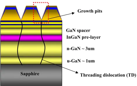
different thickness of quantum barriers. The MQW structures also had been prepared to characterize the morphology of the growth pits by atomic force microscopies (AFM), and the thickness of GaN QBs about 104Å, 57 Å and 33Å were denoted as MQW A, MQW B and MQW C respectively. Figure 2 shows the schematic figure of MQW structures which terminated at the GaN last quantum barrier.
Fig. 1. The schematic figure of epitaxial structure of light emitting diodes with different thickness of GaN quantum barriers
Fig. 2. The schematic figure of epitaxial structure of multiple quantum well which terminated at the GAN last quantum barrier.
Sapphire u-GaN ~ 1um n-GaN ~ 3um InGaN pre-layer GaN spacer … GaN last-barrier p-AlGaN InGaN/GaN MQW x 6 pairs InGaN/GaN MQW x 3piars ( GaN barrier :Si)
LED A GaN barrier ~ 104Å LED B GaN barrier ~ 53Å LED C GaN barrier ~ 33Å p-GaN Threading dislocation (TD) Sapphire u-GaN ~ 1um n-GaN ~ 3um InGaN pre-layer GaN spacer Growth pits
Proc. of SPIE Vol. 8278 82781A-2
3. RESULTS AND DISCUSSION
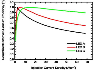
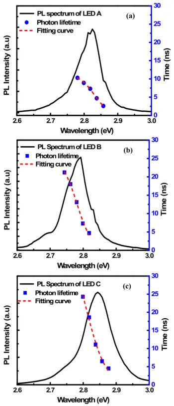
The time resolved photoluminescence (TRPL) measurement was applied to analyze the carrier life time and localization behavior at low temperature (LT) 15K, and was performed by frequency doubled femto-second-pulse Ti:sapphire laser at a wavelength of 400 nm with pumping power density 100kW/cm2. Figure 3 shows the normalized
efficiency curve as increasing the injection current density. The efficiency droop percentage is about 50%, 35%, and 10% from maximum to operation current density 70A/cm2 of LED A, B, and C respectively. The droop percentage had
been remarkably improved as reducing the thickness of GaN QBs. This significant improvement in efficiency droop can be mainly attributed to more uniform carrier distribution in the MQWs by tunneling effect of electron and hole carriers as reducing the thickness of QBs [10]. It reduces the carrier density in each QW to prevent the Auger recombination under high current density operation [5-7].
Fig. 3. Normalized external quantum efficiency versus injection current of LED A, B and C.
The PL spectra and decay time at specific emission photon energy of LEDs are shown in the figure 4, the degree of localization in InGaN MQWs and rediative recombination time can be fitted by theoretical model [11]. Fitting results are shown in the table 1. The radiative recombination time becomes longer from 13.2 to 25.1ns and localization energy becomes smaller from 30.3 to 18.7mev as reducing the thickness of GaN QBs from 104 to 33 Å. We supposed that is due to the reduction of thickness of QB reduces the potential height and the wave function of carriers have chance to penetrate through the QB into the next QW. This makes the carriers less localized in one QW and takes more time to produce radiative recombination [10], the InGaN/GaN active region may become super-lattice (SL) like properties and the mini-bands will reduce the carrier density in the active layer which prevents the efficiency droop from Auger effect at high carrier injection [5-7, 10].
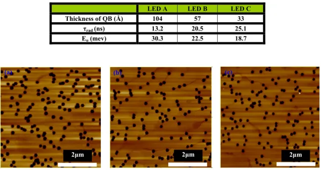
Thinner GaN QBs may have a crystalline quality issue due to most of QBs grow at temperature ramping region between the QW and QB. MQWs sample without electron blocking layer and the p-type GaN layer were also grown to characterize the pits density as well as threading dislocation (TD) density by atomic force microscopy (AFM). The v-pits were produced by InGaN/GaN hetero-interface at the position of TDs. The AFM images of MQW A, B, and C are shown in the figure 5. The depth and density of the v-pits are very close between these three samples, which mean that the TD density does not increase as the GaN QBs decreasing from 104 Å to 33 Å. The SL active structure is an effective solution to alleviate the efficiency droop properties under high current density operation.
0 10 20 30 40 50 60 70 0.0 0.1 0.2 0.3 0.4 0.5 0.6 0.7 0.8 0.9 1.0 1.1 N o rm al iz ed E xt er n al Q u an tu m E ff ici en cy ( % )
Injection Current Density (A/cm2)
LED A LED B LED C
Proc. of SPIE Vol. 8278 82781A-3
Fig. 4. Photoluminescence (PL) spectrum and PL decay time at specific emission energy of LED A, B and C at 15k. 2.6 2.7 2.8 2.9 3.0 PL spectrum of LED A Wavelength (eV) P L In te n s ity ( a .u ) 0 5 10 15 20 25 30 Photon lifetime Fitting curve Ti m e ( n s ) (a) 2.6 2.7 2.8 2.9 3.0 PL Spectrum of LED B Wavelength (eV) P L In te n sit y (a .u ) 0 5 10 15 20 25 30 Photon lifetime Fitting curve Ti m e ( n s) 2.6 2.7 2.8 2.9 3.0 PL Spectrum of LED C Wavelength (eV) P L In te n sity (a .u ) 0 5 10 15 20 25 30 Photon lifetime Fitting curve Ti m e ( n s) (b) (c)
Proc. of SPIE Vol. 8278 82781A-4
Table Ι Fitting results of degree of localization and radiative recombination time of LED A, B and C.
LED A LED B LED C
Thickness of QB (Å) 104 57 33
τrad (ns) 13.2 20.5 25.1
Eo (mev) 30.3 22.5 18.7
Fig. 5. Atomic Force Microscopy images of top surface of (a) MQW A, (b) MQW B and (c) MQW C.
Table ΙI Characterizations of V-pits of MQW A, B and C.
MQW A MQW B MQW C
Thickness of QB (Å) 104 57 33
RMS (nm) 27 22 19
V-pits density (cm-2) 6.6E8 5.4E8 5.7E8
Size of V-pits (nm) 0.27 0.24 0.26
4. CONCLUSIONS
The efficiency droop behaviors of InGaN/GaN blue LEDs with different thickness of GaN QBs were investigated in this work. The droop percentage from efficiency peak to 70 A/cm2 is only about 10% as reducing the thickness of GaN
QBs from 104 Å to 33 Å. The major contribution may due to more uniform distribution of electron and hole carrier in the SL like active region. The crystalline quality does not become worse from the results of v-pits density even thickness of GaN QBs is as low as 33 Å. The SL active structure could be an effective solution to alleviate the efficiency droop for the application of solid state general lighting.
ACKNOWLEDGEMENTS
The authors would like to thank Dr. T. C. Hsu and M. H. Shieh of Epistar Corporation for their technical supporting. This work was founded by the National Science Council in Taiwan under grant number, NSC NSC98-3114-M-009-001 and NSC99-2221-E-009-001.
2μm
(a) (b) (c)
2μm 2μm
Proc. of SPIE Vol. 8278 82781A-5
REFERENCES
[1] M. H. Crawford, ”LEDs for solid-state lighting: performance challenges and recent advances”, IEEE J. Sel. Top. Quantum Electron. 15, 1028(2009).
[2] K. J. Vampola, M. Iza, S. Keller, S. P. DenBars, and S. Nakamura, ”Measurement of electron overflow in 405nm InGaN light-emiting diode structures”, Appl. Phys. Lett. 94, 061116(2009).
[3] A. David, M. J. Grundmann, J. F. Kaeding, N. F. Gardner, T. G. Mihopoulos, and M. R. Krmes, “Carrier distribution in (0001)InGaN/GaN multiple quantum well light-emitting diodes”, Appl. Phys. Lett. 92, 053502(2008). [4] Y. C. Shen, G. O. Mueller, S. Watanabe, N. F. Gardner, A. Munkholm, and M. R. Krames, “Auger recombination in
InGaN measured by photoluminescence”, Appl. Phys. Lett. 91, 141101(2007).
[5] J. Hader, J. V. Moloney, B. Pasenow, S. W. Koch, N. Linder, and S. Lutgen, “On the importance of radiative and Auger loss in GaN-based quantum wells”, Appl. Phys. Lett. 92, 261103(2008).
[6] X. Ni, Q. Fan, R. Shimada, Ü. Özgur, and Hadis Morkoç, “Reduction of efficiency droop in InGaN light emitting diodes by coupled quantum wells”, Appl. Phys. Lett. 93, 171113(2008).
[7] E. Kioupakis, P. Rinke, K. T. Delaney, and C. G. Van de Walle, “Indirect auger recombination as a cause of efficiency droop in nitride light-emitting diodes”, Appl. Phys. Lett. 98, 161107(2011).
[8] Y. Yang, X. A. Cao, and C. Yan, “Investigation of the Nonthermal Mechanism of Efficiency Rolloff in InGaN Light-Emitting Diodes”, IEEE Trans. Eletron Devices 55, 1771(2008).
[9] B. Monemar and B. E. Sernelius, “Defect related issues in the current roll-off in InGaN based light emitting diodes”, Appl. Phys. Lett. 91, 181103(2007).
[10] K. Mukherjee and N. R. Das, “Tunneling current calculation for nonuniform and symmetric multiple quantum well structures”, J. Appl. Phys. 109, 053708(2011).
[11] S. F. Chichibu, H. Marchand, M. S. Minsky, S. Keller, P. T. Phini, J. P. Ibbetson, S. B. Fleischer, J. S. Speck, J. E. Bowers, E. Hu, U. K. Mishra, S. P. Denbaar, T. Deguchi, T. Sota, and S. Nakamura, “Emission mechanisms of bulk GaN and InGaN quantum welss prepared by lateral epitaxial overgrowth”, Appl. Phys. Lett. 74, 1460(1999).
Proc. of SPIE Vol. 8278 82781A-6