436 IEEE ELECTRON DEVICE LETTERS, VOL. 13, NO. 8, AUGUST 1992
Numerical Simulation
of
the Hysteresis in the
Sidegating Effect in GaAs MESFET’s-
The Effect
of
Schottkv Contacts
JShwu-Jing C h a n g a n d Chien-Ping Lee, Member, IEEE
Abstract-Two-dimensional simulation of the sidegating effect in GaAs MESFET’s has been performed. The result confirms that Schottky contacts on semi-insulating substrate cause seri-
ous high substrate leakage current and drain current reduction in GaAs MESFET’s. The competition between the currents or
biases of the contacts is found to be the cause of the S-type negative differential conductivity (S-NDC) or hysteresis ob- served when measuring the sidegating threshold.
YSTERESIS and S-type negative differential con-
H ductivity (S-NDC) are commonly observed when
measuring the threshold behavior of the sidegating effect in GaAs MESFET’s in the voltage-controlled condition and the current-controlled condition, respectively. These features have been explained based on impact ionization of deep traps in the substrate by Li et al. [l], [2]. However, recent studies [3]-[5] have recognized that Schottky con- tacts on the semi-insulating substrate play an important role in the sidegating effect in GaAs MESFET’s. Our previous simulation results have also shown that the Schottky contact can cause, enhance, or shield the side- gating effect [61. Therefore, the effect of the Schottky contacts should be considered in the observed hysteresis or S-NDC in the sidegating effect, as in the simulations to be presented in this letter.
For numerical simulation, a two-dimensional, two-car- rier, steady-state device simulation program based on the drift-diffusion formulation was developed. In this pro- gram, transport of free carriers is calculated by solving current continuity equations and the Poisson’s equation. The emission and capture of free carriers through deep traps in the substrate follow the Shockley-Read-Hall model. Constant electron mobility at low fields and veloc- ity saturation beyond a critical field were used for the velocity-field relationship in simulation.
The semi-insulating substrate was assumed to contain deep donors that compensate for shallow acceptors, simi- lar to the case of undoped LEC stubstrates. The proper- ties of the traps in the substrate, which include the capture cross sections and energy levels of the deep traps, Manuscript received May 12, 1992. This work was supported by the National Science Council of the Republic of China.
The authors are with the Department of Electronics Engineering and Institute of Electronics, National Chiao Tung University, Hsinchu, Tai- wan, Republic of China.
IEEE Log Number 9202474.
are summarized in Table 1. The capture cross sections used are the same as those used by Goto and Ohno [41. In addition to the EL2 like deep donors which act as elec- tron traps, deep levels acting as hole traps were also included. The existence of hole traps has been found essential to the sidegating effect [4], [6], although similar results can be obtained if t h e hole traps were deep accep- tors instead of deep donors.
In the simulation, a true sidegate configuration is adopted, where the sidegate is placed at the top surface of the substrate along with all other contact terminals as shown in Fig. 1. The FET had a 1-pm gate with a 3-pm source-to-drain spacing. The FET channel was 0.12 p m thick and was uniformly doped to 10” ~ m - ~ . The sidegate was placed 8 p m away from the FET. A 1-pm-wide Schottky bar contacting the semi-insulating substrate (i- substrate) was placed in between the sidegate and the FET, 4 p m away from the sidegate. This Schottky bar, which may be regarded as a part of the Schottky gate that extrudes out of the active region and contacts the i-sub- strate or any interconnection metal that contacts the substrate, has been found to be essential to the sidegating effect [31-[61.
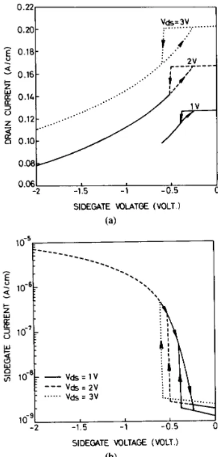
The calculated drain current I d y 5 and sidegate leakage current I,,,, as functions of the negative sidegate voltage with different drain biases Vds, are shown in Fig. 2(a) and (b), respectively. The gate, source, and the Schottky bar are all grounded. This corresponds to the voltage-con- trolled condition. It can be seen in these plots that a significant reduction of the drain current and an abrupt increase of the sidegate leakage current occur when a threshold voltage is reached. The drain current continues to drop and the leakage current continues to increase after the threshold. However, when the negative sidegate voltage is reduced after the onset of the sidegating, the sidegating characteristics (Fig. 2(a) and (b)) follow differ- ent paths and show apparent hysteresis. There are no sudden increase in the drain current and sudden decrease in the leakage current. The threshold voltages are also smaller. Both the negative threshold voltage and the amount of hysteresis increase with the drain bias. These features are in qualitative agreement with the commonly observed experimental results [ 11, [2]. (Although the struc- tures in those experimental studies may not purposely include a Schottky contact, the gate contact pad, the part of the Schottky gate that extrudes out of the active region, 0741-3106/92$03.00 0 1992 IEEE
CHANG AND LEE: SIMULATION OF HYSTERESIS IN SIDEGATING EFFECT IN GaAs MESFET'S 437
TABLE I
PROPERTIES OF TRAPS IN THE SUBSTRATE
Electron Capture Hole Capture Energy Level Concentration Cross Section Cross Section E,-E,
Cateaorv ( ~ m - ~ ) (cm2) (cm2 ) (eV) electron trap 10'6 hole trap 1015 shallow acceptor 1015 1 x 10-13 3 x 10-16 0.715 3 x 10-l6 1 x 10-13 0.745 - - - %mi-imulaling Substrate
"il
Fig. 1. The device structure used for numerical simulations. Donor concentration of the n-doped regions is 10'' C I I - ~ .
0.22 0.20 yd. .. ... 3v.:. ... . .
.
0 . w - -2 -1.5 - 1 -0.5 0SIDEGATE VOLATGE (VOLT )
(a)
2
10-8-
V d S = l V vd5 2 2 v V& = 3v---
g i
... 1 0 -9 : -2 -1.5 I -1 -0.5 0SIDEGATE VOLTAGE (VOLT.)
(b)
Fig. 2. (a) Calculated FET drain current and (b) sidegate current as functions of the sidegate voltage with the drain of the FET biased at 1 V
(solid lines), 2 V (dashed lines), and 3 V (dotted lines). The gate, source, and the Schottky bar are grounded.
or any interconnection metal which contacts the substrate can be regarded as the Schottky contact used in the simulation.) Besides, the sidegate currents increase with the drain bias before the onset of sidegating effect and become independent of the drain bias after the abrupt
increase at sidegating threshold (see Fig. 2(b)). When the negative sidegate bias is decreased again, the sidegate currents follow the same curve until their respective cur- rent levels before the onset of sidegating is reached.
Based on the above simulation results, the observed hysteresis can be explained as the result of the competi- tion between the contact currents or biases. 1) The poten- tial of the i-substrate around the Schottky bar is affected by the positive bias applied to the drain of the FET, the negative voltage applied to the sidegate, and the bias applied to the bar itself. 2) Before the application of negative sidegate voltage, the current flow through the Schottky contact is the reverse saturation current of the n(FET)-i-Schottky structure. When the applied negative sidegate voltage is small, the potential around the Schot- tky bar is dominated by the effect of the drain bias (the Schottky bar current remains to be the small reverse saturation current from the FET side) and the sidegate current is dominated by the n(FET)-i-n(sidegate) current. Only when the negative bias applied to the sidegate is large enough to overcome the effect of the drain bias of the FET does the current between the Schottky contact and the sidegate begin to flow as it should in a forward- biased Schottky-i-n(sidegate) structure. After the onset of forward Schottky-i-n current, the Schottky bar current reverses sign, increases very rapidly, and dominates the sidegate current as shown in Fig. 3. It has been shown in [6] that holes injected from this Schottky contact can be transported through the substrate to the FET side with the aid of hole traps. This extension of hole accumulation region causes the potential profile to be nearly flat in the whole i-substrate region with most of the voltage drop across the F E T s channel-substrate interface junction and results in the sidegating effect. 3) When the negative sidegate voltage is reduced after the onset of the sidegat- ing effect, the potential around the Schottky bar is pre- dominantly affected by the sidegate bias. Therefore, the sidegate characteristics continue to follow those of the forward-biased Schottky-idsidegate) structure until the current levels are reduced to those of the n(FET)-i- nhidegate) current before sidegating.
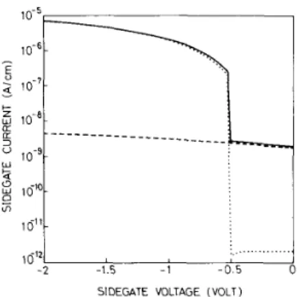
To explain the S-type negative differential conductivity (S-NDC) in the sidegating characteristics in the current- controlled measurement [ 11, [2], the current -voltage char- acteristics of the n(FET)-i-n(sidegate) were simulated with the Schottky bar (in Fig. 1) floating and the drain biased at 2 V (see Fig. 3). It is found that the resultant n(FET)-i- dsidegate) current is several orders lower than the for- ward Schottky-i-dsidegate) current after the onset of the
438 I E E E LLI ( - I R O N i)rvi( E ~b ITFR\ VOL 13. N O 8 AUGUST 1992
10-6
”F
16”}
1
SIDEGATE VOLTAGE (VOLT )
Fig. 3. Calculated sidegate current (solid line) and the value of the Schottky current (dotted line) as functions of the sidegate voltage with the Schottky bar grounded. The calculated sidegate current (dashed line) with the Schottlq bar floating is also shown for comparison. The drain of the F E T is biased at 2 V.
sidegating effect at the same sidegate voltage. Therefore, the S-NDC can be explained as follows: when a negative current (flowing out of the electrode) is applied to the sidegate as in the current-controlled measurement, the current-voltage characteristics of the sidegate would ini- tially follow those of the n(FET)-i-dsidegate) structure when the driving sidegate current is low. The Schottky bar remains reverse biased by the positive drain bias of the FET. After the driving source
(Z,\{)
has been increased to a critical level, the Schottky-i-n(sidegate) structure starts to conduct, shunts most parts of the n(FET)-i-n(sidegate) path, and dominates the sidegate current. Since the cur- rent level of the forward Schottky-i-n current is much higher than that of the n-i-n current at the same sidegate voltage, when the sidegate current is continuously in- creased as in the current-controlled measurement, there would be an abrupt decrease in the sidegate voltage at thesidegating threshold. Therefore, it is the transition of the sidegate current from the n-i-n current to the Schottky-i-n current that causes the S-NDC feature.
The recent experimental study by Liu et al. on the Schottky contact effects on the sidegating characteristics [7] has also shown results and conclusions which agree well with the above pictures of hysteresis and S-NDC drawn from our simulations.
In conclusion, we have performed two-dimensional sim- ulations on sidegating effect in GaAs MESFET’s with a realistic configuration, where both the FET and the side- gate are placed on the surface of the substrate. The simulated results are in good agreement with the observed features of hysteresis or S-NDC in the sidegating effect. The hysteresis or S-NDC associated with the threshold behavior of the sidegating effect is found to be related to the leakage current of the Schottky-i-n(sidegate) structure under the influence from the biases of the FET.
REFERENCES
Z.-M. Li. S. P. McAlistcr, W. G. McMullan, C. M. Hurd. and D. J . Day, “Impact ionization 01 deep traps in semi-insulating GaAs wbstratcs.” .I. Appl. Phys., vol. 67. pp. 7368-7372, 1990.
Z.-M. Li. D. J . Day, S . P. McAlister. and C. M. Hurd. “Inclusion of impact ionization in the backgating of GaAs FETs,” IEEE Elec-
tron fkrcr, Lrtt., vol. I 1 . pp. 342-345. 1990.
Y. Liu, R. W. Dutton, and M. D. Deal. “Sidcgating effect of GaAs M E S F E r s and leakage current in a semi-insulating GaAs sub- strate,” f E E E Electron l k r , i c e Lett., vol. 1 I . no. 1 1 , pp. 50.5-507,
1090.
N . Goto a n d Y. Ohno. “Two-dimensional simulation of GaAs MESFET d e g a t i n g effect.” in !‘roc. 5th Conf: Semi-fnsulafing
111 -V Muter.. lY88, pp. 253-258.
K. Inokuchi. Y. S . Itoh, and Y. Sano. “Influence of metal structure o n sidegating properties in GaAs LSla.” J. Electrochem. Soc.. vol. 137. no. 9. p. 404C, 1000.
S . J. Chang and C. P. Lee. “Numerical simulation of sidegating elfect in GaAs MESFETa.“ submitted to 1EEE Trans. Electron
l h .ic.es.
Y. Liu. R. W. I h t t o n . and M. D. Dcal. “Schottky contact effects in thc sidegating effect of GaAs devices,” f E E E Electron Dei,ice Lett..