Effect of different n-electrode patterns on optical characteristics of
large-area p-side down InGaN light-emitting diodes fabricated by
laser lift-off
Jung-Tang Chu, Wen-Deng Liang, Chih-Chiang Kao, Hung-Wen Huang, Chen-Fu Chu,
Hao-Chung Kuo* and S.C. Wang
Institute of Electro-Optical Engineering, National Chiao Tung University, Hsinchu, Taiwan, R.O.C.
ABSTRACT
Large-area (1000×1000 µm2) p-side down InGaN light-emitting diodes (LEDs) have been fabricated by laser lift-off (LLO) technique. The p-side down LEDs with different geometric patterns of n-electrode were fabricated to investigate electrode pattern-dependent optical characteristics. Current crowding effect was first observed in in the p-side down InGaN LLO-LEDs. The LEDs with well designed n-electrode shows a uniform distribution of light-emitting pattern and higher out put power due to uniform current spreading and minimization of thermal effect. The output power saturation induced by current crowding in the LEDs with simplest geometric n-electrode was demonstrated. In absent of transparent contact layer for current spreading, the n-electrode pattern has remarkable influence on the current distribution and consequently the light output power of the large-area p-side down LEDs.
KEYWORDS: GaN LEDs, laser lift-off (LLO), wafer bonding, large-area light-emitting LEDs
1. INTRODUCTION
GaN based devices such as light-emitting diodes (LEDs), laser diodes (LDs), and filed effect transistors (FETs) with high power operation have attracted considerable interest and have seen significant development. Especially, GaN based LEDs are being marketed and used for a variety of applications, including traffic signals, full-color displays, back lighting in liquid-crystal displays, and white LEDs. Recently, high-efficiency white LEDs made by blue LEDs and phosphor have gained much interest because the replacement of fluorescent lamps will be realistic in the near future [1]-[4]. However, for illumination applications, where dozens, hundreds or even thousands of lumens are required in a single light source, can hardly be realized by simply accumulating appropriate numbers of conventional size (about 350×350 µm2) LEDs. Therefore, the size of a single LED chip is desired to be enlarged to provide higher light output power. For GaN-based LEDs epitaxially grown on sapphire, the chip size was restricted by the low thermal conductivity of the sapphire and low conductivity of the p-type GaN. In the recently reports [5]-[9], the p-side down
GaN laser-lift-off LEDs (LLO-LEDs) on Cu substrate have been reported with superior performance over the conventional p-side up LEDs on sapphire due to eliminating the constrain of the sapphire substrate and p-GaN. The large-area light-emitting p-side down LLO-LEDs with the size of 1000×1000 µm2 on Cu substrate was also demonstrated in our previous report [10]. In the p-side down LLO-LEDs configuration, n-GaN layer serves as a better current spreading layer than p-GaN layer in the p-up configuration on sapphire substrate due to higher electron mobility and thicker thickness of n-GaN layer. However, the influence of n-electrode pattern on current spreading in the p-side down LLO-LEDs was not investigated. Since the light emission intensity is directly proportional to the current density [11], uniform current distribution in n-GaN layer for providing uniform light emitting pattern is desired. In this work, the wafer bonding and LLO techniques were used to fabricate large-area p-side down LLO-LEDs with the size of 1000×1000 µm2. Four types of different geometric n-electrode patterns were deposited on n-GaN without transparent contact layer. We first observe and study the current crowding phenomenon in the p-side down GaN LLO-LEDs under high current injection level. The light emission patterns of LEDs with different n-electrode patterns were compared. The electrode pattern dependent light output power was also discussed.
2. EXPERIMENTAL
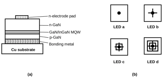
The LED structure was grown by metalorganic chemical vapor deposition on a (0001) sapphire substrate. The LED structure consists of a 4-µm-thick Si-doped GaN layer, a multi-quantum-wells (MQWs) region consisting of five pairs of In0.25GaN0.75 well (3nm) and GaN barrier (10nm), and a 0.1-µm-thick Mg-doped GaN layer. The original LED wafer with backside polished sapphire substrate was cleaved to the size of 1.5×1.5 cm2. The SixN1-x film was deposited on the samples and then patterned SixN1-x served as etching mask were defined by a standard photolithographic and etching process. The 1000×1000 µm2 mesas were then formed by inductively coupled plasma reactive ion etching. The Ni/Au/Ni (20 nm/20 nm/150 nm) layers were then deposited on the defined mesas. The first Ni/Au layers is p-GaN contact and the final Ni layer serves as the bonding metal. The LED sample with a structure of sapphire/GaN-LED/Ni/Au/Ni was then bonded with a Ni-coated Cu substrate by a fixture in argon atmosphere at 400℃ for 30 min. The bonded structure was then subjected to the LLO process. A KrF excimer laser at wavelength of 248 nm with pulse width of 25 ns was used to separate the sapphire substrate from the epitaxil LED structure. The incident laser with a beam size of 1.2 mm × 1.2 mm was incident from the polished backside of the sapphire substrate onto the sapphire/GaN interface. In this process, the beam size of KrF laser was larger than that of the size of LEDs. Therefore, the laser irradiation on the interface of sapphire and GaN was uniform. After the LLO process, the n-GaN/MQW/p-GaN/Ni/Au/Ni structure was transferred onto the Cu substrate as shown in Fig.1(a). Finally, Ti/Al layers with different patterns were deposited on n-GaN as the n-type contact without additional transparent contact layer. The top view of the LED devices with four different n-electrode patterns were shown as Fig. 1(b). The diameter of the circular electrodes centered at the mesas for the four types LEDs is 120 µm. In LED b, the width and length of the straight electrode is 20 µm and 700 µm, respectively. The dimension of the cross-shaped electrode is the same in LED b, LED c and LED d. In LED c, the width of the square is
520 µm. In LED d, the width of the inner and outer squares is 350 µm and 700 µm, respectively. 3. RESULT and DISCUSSION
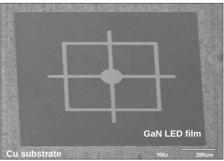
The scanning electron microscope (SEM) image of the LED c on Cu substrate was shown in Fig. 2. Complete and smooth LED film on the Cu substrate without peeling or cracks were observed despite the large different thermal expansion coefficients of GaN (4.4×10⁻⁶K-1) and Cu (16.9×10⁻⁶K-1). The smooth and well adhesive bonding interface was also obtained. These results are essential for providing good optical and electrical characteristics of the LLO-LEDs. Surface light-emitting patterns of the four LEDs with different n-electrode were shown as Fig. 3. The light-emitting patterns were obtained and analyzed at driving current of 450 mA by a near field microscope with a charge couple device (CCD) and a video analyzer linked to the computer. The solid curves in the bottom of the images stand for the relative light-output power measured along the dash lines. The relative light-output power was obtained by the BeamView Analyzer 2.2 (Coherent Inc.). The light intensity were normalized with the peak values, which are at the edges of the circular electrodes in four LEDs respectively. In Fig. 3(a), the light emission distributed near around the circular electrode showed intenser intensity, which reveals that the injection current clouded around the electrode pad. As shown by the relative intensity curve, the output power drops to 1/e of the maximum value as the distance from the edge of circular electrode increased to about 190 µm. In absence of transparent contact layer for current spreading, the n-electrode of LED a is insufficient for uniform current spreading in the large-area p-down LEDs configuration. In Fig. 3(b), the intenser light emission around the extended cross-shaped electrode was also observed. With the enhancement of the cross-shaped electrode for current spreading, the distribution of light emission was more uniform compared with LED a as show by the intensity curve. The extended cross-shaped electrode improved the current spreading over the large-area mesa and consequently provided a more uniform light emission pattern. For more extended electrode patterns, the light emission patterns were shown as Fig. 3(c) and Fig. 3(d). In Fig. 3(c), the light intensity of LED c showed decrease near the edge of the mesa, in contrast, the light intensity of LED d showed uniform distribution from the center to the edge of the mesa. The image also showed that emission pattern of LED d is more uniform compared to the emission pattern of LED c in which the intenser emission distributed inside the square electrode.
In Fig.4, the light output power-current (L-I) characteristics of the LEDs with four different n-electrode patterns were compared. This output power measurement was performed from the upper side of the chip using a large area Si photodiode placed 5mm above the test samples. All L-I curves showed linear characteristics up to 250 mA. The light output power of the four LEDs were also approximate equal when the driving current was below 250 mA. The injection current were supposed to spread uniformly over the mesas in the four LEDs, which results in the light output powers were equal as the driving current was below 250 mA. As the injection current increased above 400 mA, the light output power of LED a started to saturate and decrease due to current crowding effect as shown by the image in Fig. 3(a). In addition, the thermal effect caused by high current density distributed around the circular electrode also degraded the light output power. In LED b, the output power saturation was also observed under higher current injection level above
600 mA. The L-I curve of LED d performed superior characteristic over the other LEDs due to well designed electrode for providing uniform current spreading. The well designed electrode in LED d not only provide better current spreading but also reduce the thermal effect caused by localized high injection current density. As the injection current was driven at 1000mA, the light output power of LED d shows 1.15, 1.30 and 3.15 times larger than that of LED c, LED b and LED a, respectively.
In order to verify the thermal effect caused by high current density, the L-I characteristic of LED a under continuous-wave (cw) and pulse operation varying duty cycles were compared. As seen in Fig. 5, the output power was increased as the operation duty cycle was decreased. The result indicates that the thermal effect induced by crowed current around the circular electrode responds in power rollover of LED a.
4. CONCLUSION
In summary, we first report and observe the effect of n-electrode patterns on optical characteristics of the large-area p-side down LLO LEDs. The light emitting patterns showed obvious current crowding effect in the LEDs with non-well designed n-electrode. The LEDs with well designed n-electrode showed a uniform distribution of light-emitting pattern and higher out put power attribute to uniform current spreading resulting in minimizing thermal effect. The rollover of output power induced by current crowding effect in the LEDs was demonstrated. The geometric pattern of the n-electrode has remarkable influence on the current distribution and consequently the light output power of the large-area p-side down LEDs without transparent contact layer.
n-GaN GaN/InGaN MQW p-GaN Bonding metal (a) n-electrode pad (b) LED a LED b LED c LED d
Figure 1: The schematic structure of the p-side down LLO-LED on copper substrate (a) and top view of the LED devices with four types n-electrode patterns (b).
GaN LED film
Cu substrate
Figure 2: The SEM images of the transferred LED c on Cu substrate. No peeling or cracks were observed on the LED film.
(c) (d) (a) (b)
Figure 3: Light-emitting patterns of the p-side down LLO-LEDs with four different geometric n-electrode patterns: (a) LED a, (b) LED b, (c) LED c and (d) LED d. The solid curves in the bottom of the images stand for the relative light-output power measured along the dash lines
0 200 400 600 800 1000 1200 0 50 100 150 200 250 300 350 400 Li ght outpu t pow er (mW )
Driving current (mA) LED d
LED c LED b LED a
Figure 4: Light output power as a function of driving current for the four types p-side down LEDs.
0 100 200 300 400 500 600 700 0 2 4 6 8 10 12 14 16
Driving current (mA)
Li g ht ou tp ut po w e r ( a .u. ) 0.01% 10% CW LED a
REFERECE
[1] S. Nakamura and G. Fasol, The Blue Laser Diode, Berlin, ermany: pringer-Verlag, 1997, pp. 216–219.
[2] J. Han, M. H. Crawford, R. J. Shul, J. J. Figiel, L. Zhang, Y. K. Song, H. Zhou, and A. V. Nurmikko, “AlGaN/GaN quantum well ultraviolet light-emitting diodes,” Appl. Phys. Lett., vol. 73, no. 12, pp. 1688–1690,Sept. 1998.
[3] Y. Narukawa, I. Niki, K. Izuno, M. Yamada, Y. Murazki, and T. Mukai, “Phosphor-conversion white light-emitting diodes using InGaN near-ultraviolet chip,” Jpn. J. Appl. Phys. Lett., vol. 41, pp. L371–L373, 2002.
[4] Daniel A. Steigerwald, Jerome C. Bhat, Dave Collins, Robert M. Fletcher, Mari Ochiai Holcomb, Michael J. Ludowise, Paul S. Martin, and Serge L. Rudaz, “Illumination With Solid State Lighting Technology,” IEEE J. Select. Topics Quantum Electron., vol. 8, pp. 310-320, Mar.–Apr. 2002.
[5] W. S. Wong, T. Sands, N. W. Cheung, M. Kneissl, D. P. Bour, P. Mei, L. T. Romano, and N. M. Johnson,“Fabrication of thin-film InGaN light-emitting diode membranes by laser lift-off,” Appl. Phys. Lett. vol. 75, pp.1360-1362, (1999).
[6] C. F. Chu, C. Y. Yu, H. C. Cheng, C. F. Lin, and S. C. Wang, “Comparison of p-Side Down and p-Side Up GaN Light-Emitting Diodes Fabricated by Laser Lift-Off,” Jpn. J. Appl. Phys. vol. 42, pp. L147-L150, (2003).
[7] C. F. Chu, Fang-I Lai, Jung-Tang Chu, Chang-Chin Yu, Chia-Feng Lin, Hao-Chung Kuo, and S. C. Wang, “Study of GaN light-emitting diodes fabricated by laser lift-off technique,” J. Appl. Phys. 95, pp. 3916-3922, (2004).
[8] Dong-Sing Wuu, Shun-Cheng Hsu, Shao-Hua Huang, Chia-Cheng Wu, Chia-En Lee and Ray-Hua Horng, “GaN/Mirror/Si Light-Emitting Diodes for Vertical Current Injectionby Laser Lift-Off and Wafer Bonding Techniques,” Jpn. J. Appl. Phys. vol. 43, pp. 5239-5242, (2004)
[9] Bee Sim Tan and Shu Yuan, “Performance enhancement of InGaN light-emission diodes by laser lif-off and transfer from sapphire to copper substrate,” Appl. Phys. Lett., vol. 84, pp. 2757-2759, (2004)..
[10] Jung-Tang Chu, “Fabrication of large-area GaN based light-emitting-diodes on Cu substrate,” Jpn. J. Appl. Phys., (submitted). [11] E. F. Schubert, Light Emitting Diodes, Cambridge University Press, Cambridge, U.K., 2003, pp126