1054 IEEE ELECTRON DEVICE LETTERS, VOL. 30, NO. 10, OCTOBER 2009
Enhanced Light Extraction in Wafer-Bonded
AlGaInP-Based Light-Emitting Diodes via
Micro- and Nanoscale Surface Textured
Yea-Chen Lee, Hao-Chung Kuo, Senior Member, IEEE, Bo-Siao Cheng, Chia-En Lee, Ching-Hua Chiu,
Tien-Chang Lu, Member, IEEE, Shing-Chung Wang, Life Member, IEEE, Tien-Fu Liao, and Chih-Sung Chang
Abstract—AlGaInP-based metal-bonding light-emitting diodes
(LEDs) with micro- and nanoscale textured surface were inves-tigated. The device surface with microbowls and nanorods were formed by a chemical wet-etching and dry-etching technique for enhancing light-extraction purpose. The luminous intensity could be enhanced 65.8% under 20-mA current injection as compared with the plane surface LEDs. The maximum wall-plug efficiency was achieved 14.1% at 7.5-mA operation.
Index Terms—AlGaInP emitting diodes (LEDs),
light-extraction efficiency, metal bonding, silica nanoparticles, spin coating, surface textured.
T
HE HIGH-EFFICIENCY light-emitting diodes (LEDs) of AlGaInP-based quaternary materials with a visible spectrum from red to yellow-green are widely applied for many applications such as optical communications light source, TFT-LCD back light, traffic signal, automotive, exterior light-ing, indoor and outdoor display, decorative lightlight-ing, etc. [1], [2]. Recent years, the epitaxy quality in AlGaInP material was greatly improved and internal quantum efficiency had already approached to 90% or higher [3] by excellent epitaxy technique. However, the external quantum efficiency is limited owing to the absorbing GaAs substrate and large reflection index different between AlGaInP-based material and outside medium (air or epoxy). According to the Snall’s law, the critical angle (θc) in AlGaInP-based LEDs is approximately18◦, and therefore the most generated photons could be trapped in the device from the total internal reflection (TIR) effect. Many advanced processes have been implemented in AlGaInP LEDs for enhancing light-extraction efficiency. The AlGaInP LEDs structure having a truncated-inverted-pyramid geometry GaP substrate was demonstrated [4]. Various surface rough-ness methods were applied in chip process [5]–[8]. Several
Manuscript received May 18, 2009; revised July 13, 2009. First published September 1, 2009; current version published September 29, 2009. This work was supported in part by the MOE ATU Program and in part by the National Science Council of Republic of China in Taiwan under Contracts NSC 97-2221-E-009-030-MY2, NSC 96-2628-E-009-017-MY3, and NSC 96-2221-E-009-092-MY3. The review of this letter was arranged by Editor P. K.-L. Yu.
Y.-C. Lee, H.-C. Kuo, B.-S. Cheng, C.-E. Lee, C.-H. Chiu, T.-C. Lu, and S.-C. Wang are with the Institute of Electro-Optical Engineering, Na-tional Chiao Tung University, Hsinchu 300, Taiwan (e-mail: alenlee.eo94g@ nctu.edu.tw; [email protected]; [email protected]; timtclu@ faculty.nctu.edu.tw; [email protected]).
T.-F. Liao and C.-S. Chang are with the High Power Opto. Inc., Taichung 42827, Taiwan (e-mail: [email protected]; [email protected]).
Color versions of one or more of the figures in this letter are available online at http://ieeexplore.ieee.org.
Digital Object Identifier 10.1109/LED.2009.2028445
films which have transparent, electric conductivity, and lower refractive index properties were deposited on surface [9], [10]. The absorbing GaAs substrate was substituted by a transparent substrate of sapphire which has a geometric shaping sidewall via glue bonding and chemical etching [11], [12]. Since the devices substrate in this structure is transparent, the output light is all directions including chip sidewall and surface. In this investigation, the absorbing GaAs substrate was also substituted by a high thermal dispersion Si substrate with a high-reflection mirror interface. The major distinction of output light path between thin film and transparent substrate LEDs is surface and all directions radiation, respectively. Furthermore, microbowls array and nanorods surface-textured processes were also im-plemented in this letter, which were created using nanoparticle spin coating, and dry- and wet-etching techniques. Detailed experiment steps, device structure, performances, and results will be illustrated in subsequence paragraphs.
AlGaInP epistructure was epitaxially grown on 2-in GaAs (100) substrates by a low-pressure metal–organic chemi-cal vapor deposition system. This structure with a domi-nant wavelength (λd) at 625 nm comprised a 0.1-μm-thick n-Ga0.5In0.5P etching stop layer grown on a GaAs buffer layer, a 2-μm-thick Si doped n-(Al0.5Ga0.5)0.5In0.5P, a 0.5-μm-thick Si doped n-Al0.5In0.5P cladding layer, a 0.5- μm-thick unintentionally doped active layer with 20 periods (AlxGa1−x)0.5In0.5P/(AlyGa1−y)0.5In0.5P multiple quantum
wells, a 0.8-μm-thick Mg doped p-Al0.5In0.5P cladding layer, a 5-μm-thick Mg doped p-GaP window layer, and finally an 8-μm-thick double window layer with an ultrathin GaAs layer was inserted between the p-GaP surface window layer and p-Al0.5In0.5P cladding layer [13]. Before the metal-bonding process, the AuBe/Au array of metal dots were contacted on the p-GaP surface as a function of p-type ohmic contact. The diameter, pitch, and thickness of circular AuBe/Au metal dots are 20, 90, and 0.15 μm, respectively. A SiO2 layer with thickness equal to AuBe/Au metal was selectively deposited on the p-GaP window layer. A quarter-wave-thick indium tin oxide (ITO) was sequentially deposited. High-reflective mirror of 300-nm silver layer was deposited on the ITO layer to constitute the GaP-SiO2-ITO-Ag omnidirectional reflector structure for enhancing output power. Moreover, the Ti/W/Pt/Au multilayer was orderly stacked on Ag layer to serve a function of adhesion, barrier, and bonding metal. The surfaces of p-type Si substrate were successively deposited Ti/Au/In metal for ohmic contact and bonding material. The epiwafer was flipped and bonded to the Si substrate in 220 ◦C ambience. After metal-bonding
LEE et al.: ENHANCED LIGHT EXTRACTION IN LEDs 1055
process, absorbing GaAs substrate and the etching stop layer were removed by ammonia- and phosphoric-based chemical etchant after metal-bonding process. The AuGe alloy metal for n-type contact was deposited on the n-(Al0.5Ga0.5)0.5In0.5P
surface layer. Finally, the processed wafer was loaded into a furnace under 380◦C for 40 min in nitrogen ambiance. In this detailed investigation, there are three different surface types of LED-I, LED-II, and LED-III. The LED-I surface profile was plane and without any surface textured. The microscale surface textures having periodic arrangement were applied to LED-II surface. The microscale surface textures were produced on 2-μm-thick n-AlGaInP layer using photolithography and wet-etching process. Before microscale surface-textured process, each photoresist dots mask with 3-μm dimension and distance were arranged on surface, and then the LED-II wafer was immersed in chemical mixture solution of bromine and acetic acid for half-minute. The etched areas were appeared 5- μm-wide bowl shaped, and its maximum depth was approximately 1.2μm after anisotropic chemical etching process. The last type is LED-III, having micro- and nanoscale texture on surface and was produced using twice surface roughness process. The first step is the same as LED-II process of producing microbowls array on surface. The second step is a monolayer of silica nanoparticles as a function of hard mask was spin coating on microbowls array textured surface. The silica nanoparticles were first suspended in deionized water diluted in a solution of surfactant at a volume ratio of 5 : 1. The surfactant serves to reduce surface tension and conducing nanoparticles uni-form coating on surface. This suspension was spin coating on the wafer surface, and then wafer was submitted to thermal treatment for improving adhesion. The wafer was etched by inductive couple plasma etcher, using SiCl4 and Ar reaction gases under a fixed flow rate of 45 and 5 sccm, respectively. The nanoparticles masks were removed via dilute hydrofluoric acid, and the nanorods were formed in each microbowl. Finally, the AuGe/Au were deposited on the fractional surface for n-type contact, and an antireflection layer of SiO2 was se-lectively covered on top surface. Three different type surface profile wafers (LED-I, LED-II, and LED-III) were subjected to dicing saw scribed into 300× 300-μm chip size. Devices were packaged on TO-46 form (without an epoxy lens encapsulated), and the electrical and optical properties were measured using the Instrument System CAS140CT array spectrameter system.
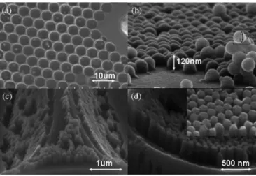
A schematic diagram of metal-bonding AlGaInP-based LED-I, LED-II, and LED-III was shown in Fig. 1, illustrating the devices structure and surface profile. Fig. 1(a) shows the LED-I device structure, having a plane surface. The microbowls shape texture (LED-II) surface and added nanorods texture covered in microbowls (LED-III) were shown in Fig. 1(b). The schematic diagram in Fig. 2(a) shows that the silica nanoparticles were spin coated on the wafer surface which was covered throughout microbowls on surface. After dry-etching and the nanomasks were removed, the nanorods were formed in microbowls surface. Fig. 3(a) shows the SEM image of the microbowl-shaped array texture on LED-II wafer surface, and each microbowl dimension of width and depth is 5 and 1.2μm, respectively. The silica nanoparticles were spin coated on wafer surface and each silica sphere diameter is 120 nm, as shown in Fig. 3(b). Fig. 3(c) and (d) shows that the nanorods were formed throughout the surface including bowl bottom, bowl
Fig. 1. Schematic diagram of the metal-bonding AlGaInP-based LEDs. (a) LED-I device structure has a plane surface. (b) LED-II device has mi-crobowls array texture on surface, and the LED-III device has added nanorods texture in microbowls.
Fig. 2. Schematic diagram. (a) Silica nanoparticles were spin coated on the wafer surface which has bowl-shaped textured. (b) Nanoscale rod was formed on surface after dry-etching process.
Fig. 3. SEM figures. (a) Microbowls array texture on LED-II surface. (b) Silica nanoparticles were spin coated on surface. (c) and (d) Nanorods were formed through wafer surface including bowl bottom, bowl sidewall, and plane surface.
sidewall, and plane surface. Fig. 4 shows the plane surface de-vices (LED-I), microbowls textured surface dede-vices (LED-II), and nanorods added in microbowls textured surface devices (LED-III) performances of forward voltage and luminous in-tensity versus injection current. With an injection current of 20 mA, the forward voltage of these LEDs are almost approx-imate 1.95 V, and luminous intensity of LED-I, LED-II, and LED-III is 240, 337, and 397 mcd, respectively. Comparing LED-I to LED-II at 20 mA, 40.8% enhancement of luminous
1056 IEEE ELECTRON DEVICE LETTERS, VOL. 30, NO. 10, OCTOBER 2009
Fig. 4. Corresponding luminous intensity–current–voltage (L–I–V ) charac-teristics of the LED-I, LED-II, and LED-III.
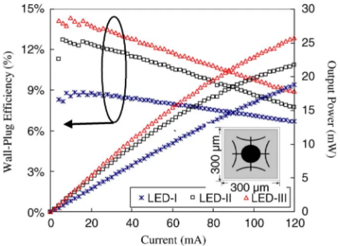
Fig. 5. LED-I, LED-II, and LED-III characteristics of the wall-plug efficiency and output power versus current.
intensity was observed and 65.8% luminous intensity enhance-ment of comparing LED-I to LED-III. The LED-III exhibits the highest luminous intensity; in other words, the LED-III has the highest light output on axis. Furthermore, the nanorods textured surface could provide 17.7% light intensity enhancement as compared with microbowls textured only surface due to the micro- and nanoscale roughness surface toward reducing TIR effect. Fig. 5 shows the output power and wall-plug efficiency (power efficiency) versus operating current. Under a 20-mA current injection, it was found that output power without epoxy resin encapsulated is 3.43, 4.83, and 5.4 mW for LED-I, LED-II, and LED-III, respectively. Although the total lumi-nous flux is the key issue for the surface-textured process, the LED-III still exhibits the maximum output power as compared with LED-I and LED-II. Comparing LED-II to LED-III at 20 mA, 11.8% enhancement of total luminous flux was observed. It means that added nanorods textured surface could increase the probability of photons escaping from semiconductor-to-air interface. In other words, LED-III has 11.8% enhancement of light-extraction efficiency was demon-strated as compared with LED-II. Furthermore, the maximum wall-plug efficiency of LED-I, LED-II, and LED-III is 8.82%, 12.74%, and 14.15%, respectively. Fig. 6 shows that the 50%
Fig. 6. Beam patterns of the LED-I, LED-II, and LED-III under 20-mA current injection.
power angle of the LED-I, LED-II, and LED-III is 115.4◦, 107.7◦, and 102.2◦, respectively. According to Fig. 6 results, the LED-III with highest luminous intensity was established on axis once again.
REFERENCES
[1] M. R. Krames, O. B. Shchekin, R. Mueller-Mach, L. Zhou, G. Harbers, and M. G. Craford, “Status and future of high-power light-emitting diodes for solid-state lighting,” J. Display Technol., vol. 3, no. 2, pp. 160–175, Jun. 2007.
[2] G. Harbers, S. Bierhuizen, and M. R. Krames, “Performance of high power light-emitting diodes in display applications,” J. Display Technol., vol. 3, no. 2, pp. 98–109, Jun. 2007.
[3] P. Altieri, A. Jaeger, R. Windisch, N. Linder, P. Stauss, R. Oberschmid, and K. Streubel, “Internal quantum efficiency of high-brightness AlGaInP light-emitting devices,” Appl. Phys. Lett., vol. 98, no. 8, p. 086 101, Oct. 2005.
[4] M. R. Krames, M. Ochiai-Holcomb, G. E. Höfler, C. Carter-Coman, E. I. Chen, I.-H. Tan, P. Grillot, N. F. Gardner, H. C. Chui, J.-W. Huang, S. A. Stockman, F. A. Kish, M. G. Craford, T. S. Tan, C. P. Kocot, M. Hueschen, J. Posselt, B. Loh, G. Sasser, and D. Collins, “High-power truncated inverted pyramid (AlxGa1-x)0.5In0.5P/GaP light-emitting diodes exhibiting>50% external quantum efficiency,” Appl. Phys. Lett., vol. 75, no. 16, pp. 2365–2367, Oct. 1999.
[5] R. Windisch, B. Dutta, M. Kuijk, A. Knobloch, S. Meinlschmidt, S. Schoberth, P. Kiesel, G. Borghs, G. H. Döhler, and P. Heremans, “40% efficient thin film surface textured light emitting diodes by optimization of natural lithography,” IEEE Trans. Electron Devices, vol. 47, no. 7, pp. 1492–1498, Jul. 2000.
[6] Y. J. Lee, T. C. Lu, H. C. Kuo, S. C. Wang, T. C. Hsu, M. H. Hsieh, M. J. Jou, and B. J. Lee, “Nano-roughening n-side surface of AlGaInP-based LEDs for increasing extraction efficiency,” Mater. Sci. Eng. B, vol. 138, no. 2, pp. 157–160, Mar. 2007.
[7] T. Kim, P. O. Leisher, A. J. Danner, R. Wirth, K. Streubel, and K. D. Choquette, “Photonic crystal structure effect on the enhancement in the external quantum efficiency of a red LED,” IEEE Photon. Technol.
Lett., vol. 18, no. 17, pp. 1876–1878, Sep. 2006.
[8] T. P. Chen, C. L. Yao, C. Y. Wu, J. H. Yeh, C. W. Wang, and M. H. Hsieh, “Recent developments in high brightness LEDs,” Proc. SPIE, vol. 6910, p. 691 005, 2008.
[9] M.-C. Wu, J.-F. Lin, M.-J. Jou, C.-M. Chang, and B.-J. Lee, “High relia-bility of AlGaInP LEDs with efficient transparent contacts for spatially uniform light emission,” IEEE Electron Device Lett., vol. 16, no. 11, pp. 482–484, Nov. 1995.
[10] Y. K. Su, H. C. Wang, C. L. Lin, W. B. Chen, and S. M. Chen, “Im-provement of AlGaInP light emitting diode by sulfide passivation,” IEEE
Photon. Technol. Lett., vol. 15, no. 10, pp. 1345–1347, Oct. 2003.
[11] Y.-C. Lee, C.-E. Lee, H.-C. Kuo, T.-C. Lu, and S.-C. Wang, “Enhancing the light extraction of AlGaInP-based light-emitting diode fabricated via geometric sapphire shaping,” IEEE Photon. Technol. Lett., vol. 20, no. 5, pp. 369–371, Mar. 2008.
[12] Y.-C. Lee, H.-C. Kuo, C.-E. Lee, T.-C. Lu, and S.-C. Wang, “High perfor-mances(AlxGa1−x)0.5In0.5P-based flip-chip light-emitting diode with a geometric sapphire shaping structure,” IEEE Photon. Technol. Lett., vol. 20, no. 23, pp. 1950–1952, Dec. 2008.
[13] K.-H. Huang, “Efficient light emitting diodes with modified window layers,” U.S. Patent 5 359 209, Oct. 25, 1994.