Electron
field emission properties on ultra-nano-crystalline diamond coated
silicon nanowires
Yu-Fen Tzeng
a, Chi-Young Lee
b,⁎
, Hsin-Tien Chiu
c, Nyan-Hwa Tai
a, I-Nan Lin
da
Department of Materials Science & Engineering, Materials Science, and Microsystems, National Tsing Hua University, Taiwan, Republic of China
bCenter for Nanotechnology, Materials Science, and Microsystems, National Tsing Hua University, Taiwan, Republic of China c
Department of Applied Chemistry, National Chiao Tung University, Taiwan, Republic of China
d
Department of Physics, Tamkang University, Taiwan, Republic of China
A B S T R A C T
A R T I C L E I N F O Available online 3 April 2008 Keywords:
Electronfield emission properties Ultra-nano-crystalline diamond (UNCD) Silicon nanowires (SiNWs)
UNCD nano-emitters
Ultra-nano-crystalline diamond (UNCD) nano-emitters were prepared by coating UNCDfilms on the tip of silicon nanowire (SiNW) templates by microwave plasma-enhanced chemical vapor deposition process. The electronfield emission properties of the UNCD/SiNW nano-emitters varied markedly with the pre-seeding process for the SiNW-templates. The direct ultrasonication process is more efficient in the formation of the diamond nuclei than the carburization/ultrasonication process, yielding UNCD/SiNWs nano-emitters with better electronfield emission properties. The electron field emission can be turned on at (E0)UNCD/SiNW4= 3.75 V/µm, yielding a large electronfield emission current density of (Je)UNCD/SiNW4= 11.22 mA/cm2at an appliedfield of 9.75 V/µm. These characteristics are significantly better than those of bare SiNWs or planar UNCDfilms.
© 2008 Elsevier B.V. All rights reserved.
1. Introduction
Diamondfilms have been widely studied for use in electron field emitters in vacuum microelectronics devices because of the negative electron affinity with low effective work functions[1]. However, the electronfield emission properties of these materials are inferior to those of carbon nanotubes (CNTs) because a large electric field is required to trigger the electronfield emission[2]. Therefore, reducing the turn-onfield of diamond films is the most urgent task. Numerous approaches have been developed to enhance the electron field emission properties of the diamond films, including reducing the size of the grains in diamonds[3], increasing the conductivity of the diamonds by doping semiconducting species[4], and fabricating the diamond tips through the utilization of high aspect ratio templates[5]. The aligned silicon tip arrays, which were used as templates for synthesizing diamond tips, have been prepared by conventional chemical vapor deposition, laser ablation and thermal evaporation/ decomposition, along with the microelectronic processes [6–8]. However, most of these approaches requires sophisticated appara-tuses and complex processing steps, which are time consuming and expensive. Recently, we developed an electrochemical process for fabricating aligned silicon nanowires (SiNWs)[9,10]. Such a process is simple and can be scaled up to fabricate aligned silicon nanowires (SiNWs) over a large area on a single-crystal silicon wafer.
In this work, we used SiNWs as a template to grow ultra-nanocrystalline diamond (UNCD) films to synthesize UNCD nano-emitters. The effect of the pre-seeding process on the growth behavior of UNCDfilms on these SiNWs and the related electron field emission properties of UNCD/SiNWs emitters were studied.
2. Experimental
Silicon nanowires (SiNWs) were fabricated by electroless metal deposition (EMD), in which (i) the [100] silicon wafer (1 × 1 cm2) was
sputter-coated with a thin goldfilm (~10 nm), and then post-annealed in an atmosphere of argon at 1073 K for 2 h to produce small gold nanoparticles (~ 15 nm) on the Si-substrate; (ii) the Si wafer was then immersed into an HF-based etching solution (12 ml of 48% HF and 0.103 M of AgNO3) for 30 min, followed by cleaning using nitric acid
and deionized water, and then dried. Self-aligned SiNWs with a diameter of about 35 nm were thus formed on Si-substrate by anisotropic etching. To study the effect of pre-seeding process on the growth behavior of UNCDfilms, some of the SiNWs were pretreated by either (i) directly ultrasonication in nanodiamond (~ 30 nm) slurry (designated as D-seeding process) or (ii) carburization by MPECVD using a high CH4concentration for 30 min, followed by ultrasonication
in nanodiamond (~30 nm) slurry for 30 min (designated as C-seeding process). UNCDfilms were deposited on the un-treated or pre-seeded SiNW-templates by MPECVD for 2 h (IPLAS, cyrannus), at the methane pressure of 100 Torr and the argon gasflow rate of 1 and 99 sccm. The microwave power was 600 W (2.45 GHz) and the reaction temperature was about 673 K.
Diamond & Related Materials 17 (2008) 1817–1820
⁎ Corresponding author.
E-mail address:[email protected](C.-Y. Lee).
0925-9635/$– see front matter © 2008 Elsevier B.V. All rights reserved. doi:10.1016/j.diamond.2008.03.023
Contents lists available atScienceDirect
Diamond & Related Materials
j o u r n a l h o m e p a g e : w w w. e l s e v i e r. c o m / l o c a t e / d i a m o n dThe morphologies of the SiNWs and UNCD nanowires were studied using SEM (JEOL JSM-6500F), whereas the crystalline structure of these nanowires was examined by high-resolution transmission electron microscopy (HRTEM, JEOL JEM-4000EX). The structure of the diamond nanowires was investigated further by Raman spectro-scopy (Renishaw, 514.5 nm). The electronfield emission properties of the UNCD nanowires were measured using a tunable parallel plate set-up, in which the sample-to-anode distance was tunable. The current–voltage (I–V) characteristics were measured using an electro-meter (Keithley 237) at a pressure of less than 10− 6Torr. The electron field emission parameters were determined from the obtained I–V curves using the Fowler–Nordheim model[11–12].
3. Results and discussions
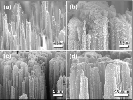
The SEM micrographs inFig. 1(a) present the morphology of the UNCD coated on bare SiNWs that were designated UNCD/SiNW1. This figure shows that the UNCD film can be grown directly on the bare SiNW-templates, indicating that the as-etched SiNWs surface contains abundant active sites, ready for reacting with carbon species in the plasma to produce diamond nuclei. However, the coating of UNCD on these SiNWs is not uniform. In some areas, the UNCD grains can fully cover the SiNWs, forming a continuousfilm, while in the others, only discrete UNCD grains are formed. This phenomenon is similar to the formation of UNCD on the bare Si-substrates without any pretreat-ment[13], which can be ascribed to the insufficient number density of diamond nuclei formed to the SiNWs template.
To facilitate the formation of diamond nuclei so as to improve the coverage and uniformity of the granular structure of UNCD grains on the SiNWs, either direct ultrasonication (D-seeding process) or pre-carbonization ultrasonication (C-seeding process) or was adopted.
Fig. 1(b) and (c) display the morphology of UNCDfilms coated on the SiNW-templates that had been pretreated by D-seeding or C-seeding processes, respectively. Thus obtained nanowires are designated UNCD/SiNW2 and UNCD/SiNW3, respectively. These micrographs indicate that both pre-seeding processes result in substantially better coverage of the UNCD grains on the SiNWs. The UNCD grains covered almost all of the SiNWs when deposited for 2.0 h. These results can
apparently be attributed to the denser diamond nuclei formed before the growth of UNCDfilms.
Fig. 2shows the typical Raman spectra obtained using a 514 nm laser. It includes broad peaks of D-band resonance near 1350 cm− 1and G-band resonance near 1550–1600 cm− 1, which typical characteristics
for diamondfilms with ultra small grain size. The Raman spectra of the UNCDfilms also include D⁎-, G⁎-band near 1150 and 1480 cm− 1, which
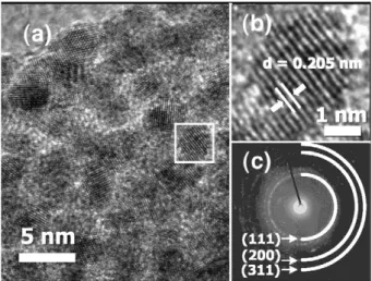
are indicated the formation of transpoly-acetylene surround the nano-sized diamond grains.[14,15] The broaden Raman resonance peaks makes the identification on the nature of the nano-grains by Raman spectroscopy extremely difficult. Examination using transmission electron microscopy (TEM) is necessary to unambiguously identify the nature of these materials.Fig. 3(a) presents the typical HRTEM micrographs of UNCDfilms grown on SiNW-templates, suggesting that thefilms contain very small grains (~5 nm). The enlarged image, which shows the lattice fringe of one of the grains (Fig. 3)(b), and selected area electron diffraction (SAED) patterns (Fig. 3)(c) demonstrate that these grains are diamonds. These observations are consistent with the literature reports[16].
Fig. 1. SEM micrographs for UNCD/SiNWs fabricated by deposition of ultra-nano-crystalline diamond (UNCD) on silicon nanowire (SiNW) arrays by a microwave-plasma-enhanced chemical vapor deposition process. (a) UNCD/SiNW1, (b) UNCD/SiNW2, (c) UNCD/SiNW3, and (d) UNCD/SiNW4. The SiNW1 is un-treated (MPECVD for 2 h); SiNW2 is pre-seeded by C-process (MPECVD for 2 h); SiNW3 and SiNW4 are pre-seeded by D-process (MPECVD for 2 h and 3 h, respectively).
Fig. 2. Raman spectra of UNCD/SiNWs, (a) UNCD/SiNW1, (b) UNCD/SiNW2, and (c) UNCD/SiNW3.
The bare SiNWs templates containing no UNCD-coatings require a very large turn-onfield, (E0)SiNW= 8.6 V/µm, to induce electronfield
emission, yielding only (Je)SiNW= 4 mA/cm2 in an applied field of
(Ea)SiNW= 22.0 V/µm (not shown). Additionally, the field
enhance-ment factor of the SiNWs is estimated as βSiNW= 367, which is
markedly smaller than the expectedβ-value of the nano-sized SiNWs and was attributed to the electrical screening effect [17]. Fig. 4
illustrates the beneficial effect of UNCD-coatings on improving the electron field emission (EFE) properties of SiNWs. Fig. 4 (open squares) indicates that the electronfield emission of UNCD/SiNW1 can be turned on at (E0)UNCD/SiNW1= 7.4 V/µm, which does not differ
significantly from E0 for bare SiNWs. However, the EFE current
density reaches (Je)UNCD/SiNW1= 11.22 mA/cm2in an appliedfield of
16.00 V/µm, which markedly exceeds the electron field emission current density of bare SiNWs.
The EFE properties of UNCD/SiNWs were significantly improved when the SiNWs were pre-seeded prior to the deposition of UNCD films. The turn-on field (E0) for inducing the electronfield emission is
reduced to 5.0 V/µm for UNCD/SiNW2 (solid circles,Fig. 4) and to 4.4 V/µm for UNCD/SiNW3 (solid triangles,Fig. 4). The pre-seeding processes, although do not substantially reduce the turn-onfield (E0),
they do tremendously improve electronfield emission current density (Je).Fig. 4indicates that the thresholdfield (Et) for UNCD/SiNW2 is
(Et)UNCD/SiNW2= 11.75 V/µm and that for UNCD/SiNW3 is (Et)UNCD/SiNW3=
11.60 V/µm, where the thresholdfield (Et) is designated as the applied
field required to induce an electron emission current density of 11.22 mA/cm2. These E
t-values are substantially lower that of
UNCD/SiNW1 to induce the same current density ((Et)UNCD/SiNW1=
16.00 V/µm).Table 1summarizes the electronfield emission pro-perties of these UNCD/SiNWs. Notably, in an applied field of Ea=
9.75 V/µm, where the UNCD/SiNW3 exhibits a large EFE current density ((Je)UNCD/SiNW3= 1.57 mA/cm2), the UNCD/SiNW2 emits only
(Je)UNCD/SiNW2= 0.59 mA/cm2 and UNCD/SiNW1 is essentially
non-emitting ((Je)UNCD/SiNW1b0.05 mA/cm2).
Apparently, the improvement on the EFE properties of UNCD/ SiNWs resulted from the pre-seeding process can be attributed to the improved coverage of UNCD grains on the SiNWs, which enhances the transport of electrons from Si to UNCD materials. For the UNCD grown on bare SiNWs, few clusters of diamond nuclei are formed because of insufficient nucleation sites are available. There exist voids among the UNCD grains and near the UNCD-to-Si interface, resulting in poor electrical contact among the UNCD grains and between the UNCD and Si-substrates. Both D- and C-seeding processes promoted nucleation kinetics of diamonds on SiNWs and can effectively eliminate the presence of voids, improving the EFE behavior markedly. However, detailed examination on the EFE characteristics of these UNCD/SiNWs indicated that the D-seeding process leads to slightly better EFE properties, as compared with the C-seeding process (cf.Table 1). The probable cause is that the carburization in C-seeding process yielded an amorphous carbon between UNCD and SiNWs, resulting in some contact resistance and inducing a fraction of the voltage drop at the UNCD-to-Si interface, such that the apparent turn-onfield is slightly larger and the attained EFE current density is smaller for the UNCD/ SiNW2, as compared with those of UNCD/SiNW3.
To improve further the electronfield emission properties of UNCD/ SiNWs, the MPECVD process was extended to 3 h on the D-process (direct ultrasonication) pre-seeded SiNW-template, UNCD/SiNW4. The morphol-ogy of UNCD/SiNW4 (Fig.1)(d) is very similar to that of UNCD/SiNW3films that were deposited for only 2.0 h (cf.Fig. 1)(b). The UNCD grains also completely cover the SiNWs. The UNCD grains are slightly larger. The Raman spectrum of UNCD/SiNW4 is similar to those of other UNCD/SiNWs and the diamond nature is also verified by TEM (not shown). The UNCD/ SiNW4 exhibits substantially better electronfield properties than that of other UNCD/SiNWs (Fig. 4, solid diamonds symbols). The UNCD/SiNW4 can be turned on at E0=3.75 V/µm and the threshold applicationfield (Et)
that yields Je=11.22 mA/cm2is Et=9.75 V/µm, which is the lowest among
all of the UNCD/SiNWs. The electronfield emission properties of UNCD/ SiNW4 are superior to those of other UNCD/SiNWs, which is apparently owing to the better UNCD-to-Si contact and denser packing of UNCD on SiNW-templates.
4. Conclusion
UNCD/SiNW field emitters were fabricated by MPECVD using SiNWs as templates. The TEM image and SAED of the coating on SiNWs
Fig. 3. Typical (a) HRTEM micrograph of UNCD/SiNW, (b) an enlarged micrograph for a single grain and (c) the SAED pattern.
Fig. 4. Electronfield emission properties, the current density-field (J–E) plots, of UNCD/ SiNWs (the insets are the corresponding Fowler–Nordheim plots). The SiNW1 is un-treated (MPECVD for 2 h); SiNW2 is pre-seeded by C-process (MPECVD for 2 h); SiNW3 and SiNW4 are pre-seeded by D-process (MPECVD for 2 h and 3 h, respectively).
Table 1
Electronfield emission properties of the UNCD/SiNWs
UNCD/SiNW1d UNCD/SiNW2d UNCD/SiNW3d UNCD/SiNW4d
Je(mA/cm2)a 0.05 0.59 1.57 11.22
Et(V/µm)b 16.00 11.75 11.60 9.75
E0(V/µm)c 7.40 5.00 4.40 3.75
aJ
e:the electronfield emission current density achieved at 9.75 V/µm applied field.
b
Et:the electricfield necessary for attaining Je= 11.22 mA/cm2.
c
E0:the turn-onfield derived from Fowler–Nordheim plots, as the interceptions of
straight lines extrapolated from the low-field and high-field segments of the F–N plots.
d
SiNW: SiNW1 is un-treated (MPECVD for 2 h); SiNW2 is pre-seeded by C-process (MPECVD for 2 h); SiNW3 and SiNW4 are pre-seeded by D-process (MPECVD for 2 h and 3 h, respectively).
1819 Y.-F. Tzeng et al. / Diamond & Related Materials 17 (2008) 1817–1820
reveal that the grains, about 5 nm in size, are diamonds. The densely populated granular structure of the thus obtained UNCD/SiNW4, which were prepared by direct ultrasonication seeding and MPECVD for 3 h, exhibit good electronfield emission properties. i.e., with a turn-onfield of (E0)UNCD/SiNW4= 3.75 V/µm and an electronfield emission
current density of (Je)UNCD/SiNW4= 11.22 mA/cm2in an appliedfield of
9.75 V/µm, which are similar to those of carbon nanotubes. The exceptional electron field emission properties of UNCD/SiNW4, as compared with the other UNCD/SiNWs, are ascribed to the better coverage of the UNCD grains over the SiNWs, and the correspondingly higher transport efficiency of electrons from Si to UNCD materials. Acknowledgements
The authors would like to thank the National Science Council, R.O.C., Taiwan, forfinancially supporting this research under Contract No. NSC 95-2113-M-007-030 and NSC 95-2112-M-032-005. Ted Knoy is appre-ciated for his editorial assistance.
References
[1] F.J. Himpsel, J.A. Knapp, J.A. Vanvechten, D.E. Eastman, Phys. Rev. B 20 (1979) 624. [2] Z. Xu, X.D. Bai, E.G. Wang, Z.L. Wang, Appl. Phys. Lett. 87 (2005) 163106.
[3] X. Lu, Q. Yang, W. Chen, C. Xiao, A. Hirose, J. Vac. Sci. Technol. B 24 (2006) 2575. [4] K. Okano, S. Koizumi, S.R.P. Silva, G.A.J. Amaratunga, Nature 381 (1996) 140. [5] Z.L. Wang, Q. Luo, J.J. Li, Q. Wang, P. Xu, Z. Cui, C.Z. Gu, Diamond. Relat. Mater. 15
(2006) 631.
[6] J. Liu, V.V. Zhirnov, G.J. Wojak, A.F. Myers, W.B. Choi, J.J. Hren, S.D. Wolter, M.T. McClure, B.R. Stoner, J.T. Glass, Appl. Phys. Lett. 65 (1994) 2842.
[7] J.C. She, S.E. Huq, J. Chen, S.Z. Deng, N.S. Xu, J. Vac. Sci. Technol. B 17 (1999) 592. [8] N.A. Kiselev, J.L. Hutchison, V.V. Roddatis, A.N. Stepanova, L.L. Aksenova, E.V.
Rakova, E.S. Mashkova, V.A. Molchanov, E.I. Givargizov, Micron 36 (2005) 81. [9] K.Q. Peng, Y.J. Yang, S.P. Gao, J. Zhu, Adv. Mater. 14 (2002) 1164.
[10] Y.F. Tzeng, K.H. Liu, Y.C. Lee, C.Y. Lee, H.T. Chiu, I.N. Lin Nanotechnology 18 (2007) 435703.
[11] R.H. Fowler, L.W. Nordhlim, Proc. Roy. Soc. London, Ser A 119 (1928) 173. [12] L.W. Nordhlim, Proc. Roy. Soc. London, Ser A 121 (1928) 626.
[13] Li-Ju Chen, Nyan-Hwa Tai, Chi-Young Lee, I-Nan Lin, J. Appl. Phys. 101 (2007) 064308.
[14] S.R. Sails, D.J. Gardiner, M. Bowden, J. Savage, D. Rodway, Diam. Relat. Mater. 5 (1996) 589.
[15] C. Ferrari, J. Robertson, Phys. Rev. B 63 (2001) 121405.
[16] L.C. Qin, D. Zhou, A.R. Krauss, D.M. Gruen, Nanostruct. Mater. 10 (1998) 649. [17] Y.F. Tzeng, Y.C. Lee, C.Y. Lee, I.N. Lin, H.T. Chiu Appl. Phys. Lett. 91 (2007) 063117.