S0013-4651(99)04-046-X CCC: $7.00 © The Electrochemical Society, Inc.
As device dimensions in ultralarge-scale integrated (ULSI) cir-cuits are scaled down to deep submicron, the interconnect delay becomes the major performance-limiting factor.1 Interconnect wire parasitics (wire resistance R and capacitance, C) have come to play a dominant role in determining not only the total signal delay but also the packing density, reliability, and manufacturing cost of integrated circuits (ICs). Because of increasingly smaller metal cross sections and reduced wire spacing, it is necessary to reduce RC through the use of new materials to limit the number of metal levels and keep the metal pitch tight. In addition, it has been reported that Cu/low-K (low-dielectric-constant) designs in 0.13 mm technology require only six metal levels to maintain a constant RC, compared to 12 levels in the Al/SiO2 system.2 More interconnect levels need more process steps, and each additional step reduces final production yield. There-fore, integration of Cu metallization and low-K dielectrics has been regarded as a promising antidote to alleviate the issues of driving speed, noise tolerance, and power dissipation in view of their respec-tive inherent benefits such as low electrical resistivity, superior elec-tromigration resistance, and low dielectric constant.
Before successful integration of the Cu/low-K system, however, a number of issues have to be addressed. First, with foreseeing dam-ascene structures for Cu, a thin barrier layer is needed to encapsulate the Cu line in three sides so as to foster adhesion and avoid Cu out-diffusion through the interlevel dielectric.1As device dimensions move to 0.25 mm and below, it becomes inappropriate to use a bar-rier layer thicker than 30 nm because a thick barbar-rier liner may lead to a high line resistance, and thus negate the advantage of low Cu resistivity. Refractory metals and their compounds have been regard-ed as attractive candidates for barrier layers because of their high thermal stability and good electrical conductivity.3-5 Specifically, tantalum (Ta) and tantalum nitride (TaN) films have recently attract-ed much interest in serving as future mainstream barrier layers.2,6,7 It is well known that Ta forms no compound with Cu and that TaN possesses a dense microstructure as well as a high melting point of 30878C. There are many studies concerning the barrier capability of Ta-based barrier layers between Cu and Si substrate8-10as well as Cu and SiO2dielectric.11,12However, no work has been reported on the study of integrating the barrier layers with Cu and low-K dielectrics. Second, organic polymers that have K values between 2.0 and 3.0 entail attractive alternatives to SiO2. However, there are still many reliability issues concerning material properties, such as low thermal stability, high thermal expansion coefficient, and low glass transition
temperature that may raise concern about the film’s mechanical strength during continuous high-temperature thermal cycles.13,14All these properties induce great challenges in process integration; nonetheless, their impacts on the device’s electrical properties have seldom been explored.
In this work, we investigate the barrier effectiveness of very thin Ta and TaN films (25 nm) in Cu/barrier/low-K-dielectric/Si metal-insulator semiconductor (MIS) capacitors and propose a novel dielectric outgassing mechanism to clarify the premature degrada-tion of Ta barriers.
Experimental
The samples used in this study were Cu/low-K-dielectric/Si MIS capacitors with and without a 25 nm thick Ta or TaN barrier layer sandwiched between the Cu and the low-K dielectric layers. Figure 1 shows the schematic cross section of the MIS samples. The low-K dielectric layers are Schumacher poly(arylene ether) (PAE-2, K 5 2.8) films,15 which were spin-on coated on a (100)-oriented p-type Si wafer to a thickness of 495 nm. A curing step was performed at 4258C in a 20% O2/80% N2ambient to cross-link the PAE-2 that increased the glass transition temperature (Tg) and the structural rigidity above
Tg. A Ta or TaN barrier layer of 25 nm thickness was sputter deposit-ed on the PAE-2 dielectric layer using a dc magnetron sputtering sys-tem with a base pressure of 1-2 3 1026Torr and no intentional sub-strate heating. The Ta barrier was sputtered from a Ta target (purity 99.95%) in Ar ambient at a pressure of 7.6 mTorr, while the TaN bar-rier was reactively sputtered using the same Ta target in a gas mixture of Ar and N2with Ar/N2flow rates of 24/6 sccm at the same pressure of 7.6 mTorr.16Prior to each sputter deposition, the target was cleaned by presputtering with the shutter closed for 10 min. The Ta and TaN films were deposited at a sputtering power of 150 W, and the deposi-tion rates of Ta and TaN were determined to be 21 and 16 Å/min,
Electrical Reliability Issues of Integrating Thin Ta and TaN Barriers with
Cu and Low-K Dielectric
Zhen-Cheng Wu,
aChau-Chiung Wang,
aRen-Guay Wu,
aYu-Lin Liu,
aPeng-Sen Chen,
aZhe-Min Zhu,
aMao-Chieh Chen,
a,*
,zJiann-Fu Chen,
bChung-I Chang,
band Lai-Juh Chen
b aDepartment of Electronics Engineering, National Chiao-Tung University, Hsinchu, TaiwanbERSO/ITRI, Deep Submicron Technology Division, Chutung Hsinchu, Taiwan
This work investigates the integration of very thin sputtered Ta and reactively sputtered TaN barriers with Cu and a low-dielectric-constant (low-K) layer of poly(arylene ether) (PAE-2). It is found that Cu readily penetrates into PAE-2 and degrades its dielectric strength in metal-insulator semiconductor capacitors of Cu/PAE-2/Si structure at temperatures as low as 2008C. Very thin Ta and TaN films of 25 nm thickness sandwiched between Cu and the low-K dielectric served as effective barriers during a 30 min ther-mal annealing at temperatures up to 400 and 4508C, respectively. We propose a failure mechanism of outgassing induced gaseous stress of PAE-2 under the Ta film to explain its premature barrier degradation. The TaN barrier did not suffer from this gaseous stress problem because of its stronger adhesion to PAE-2 than that of Ta to PAE-2, leading to a better long-term reliability. © 1999 The Electrochemical Society. S0013-4651(99)04-046-X. All rights reserved.
Manuscript received April 13, 1999.
* Electrochemical Society Active Member.
respectively. After the barrier-layer deposition, Cu film of 200 nm thickness was deposited on the barrier metal without breaking the vac-uum. Finally, the Cu surface was covered with a 20 nm thick TaN overlayer for the prevention of Cu oxidation in the subsequent high-temperature process. A lift-off process was used to define the metal gate in a circular area of 0.8 mm diam. For comparison, control sam-ples with a dielectric layer of thermal SiO2(500 nm) in place of PAE-2 (TaN/Cu/(Ta, TaN)/SiO2/Si) as well as control samples of Al-gated Al/PAE-2/Si structure were also prepared. Moreover, a 500 nm thick Al layer was deposited on the back side of Si substrates for all sam-ples for a better contact in electrical measurements.
For the thermal stability study, the MIS capacitors were thermally annealed at various temperatures for 30 min in N2ambient. The time-zero dielectric breakdown of the low-K PAE-2 films was measured by applying a voltage ramp stress using an HP4145B semiconductor parameter analyzer with the MIS capacitors biased at accumulation polarity. The breakdown voltage (Vbd) is defined as the voltage at which the capacitor’s leakage current density exceeds 1 nA/cm2, and at least 25 capacitors were measured in each category to construct the breakdown statistics.
For material analysis, unpatterned samples of (Ta, TaN)/PAE-2/Si and TaN/Cu/(Ta, TaN)/PAE-2/Si structures were prepared. These sam-ples were processed in the same process run with the MIS samsam-ples used for electrical measurements. Both film thickness and refractive index (RI) of the PAE-2 film were measured using a well-calibrated N&K analyzer at 6328 Å wavelength. X-ray diffraction (XRD) analy-sis using a 30 keV Cu Ka radiation was employed for phase identifi-cation. Field emission scanning electron microscopy (FESEM) was employed to observe the surface morphology and microstructure. Secondary ion mass spectroscopy (SIMS) was used to measure the elemental depth profiles. Fourier transform infrared spectroscopy (FTIR) as well as thermal desorption mass spectroscopy (TDS) was used to monitor the outgassing behavior of PAE-2 films during the thermal annealing process. The adhesion strength between barrier layer and PAE-2 was measured by a stud pull test using nail-shaped studs epoxy bonded to the Ta or TaN surface.
Results and Discussion
Physical property of PAE-2, Ta, and TaN.—Figure 2 shows the
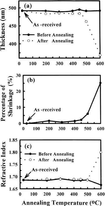
variation of thickness and refractive index of PAE-2 films thermally annealed at various temperatures. The film thickness remained near-ly constant after thermal annealing at temperatures up to 4508C; however, it shrank fiercely after annealing at and above 5008C, implying the changes of film composition and bonding structure in the PAE-2 films. As for the refractive index, it remained nearly con-stant up to 5008C but increased drastically to a value of 1.80 after annealing at 6008C. We conclude that the intrinsic PAE-2 film is thermally stable at temperatures up to 4508C, which is the ultimate thermal annealing temperature at which the devices’ electrical assess-ments were conducted.
The crystallographic structures of the as-deposited Ta and TaN barrier layers were identified to be b-Ta and cubic TaN, respective-ly, while the sheet resistances of the 25 nm thick Ta and TaN films were determined to be 72.3 and 1100 V/h, respectively. The atom-ic nitrogen concentration in the TaN film is about 20% as determined by Auger electron spectroscopy (AES) analysis. It was reported that b-Ta and cubic TaN phases exhibited superb barrier properties in the structures of Cu/(Ta, TaN)/p1-n junction diodes10 and Cu/(Ta, TaN)/SiO2/Si MOS capacitors.11
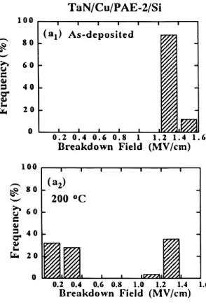
TaN/Cu/PAE-2/Si capacitors.—Figure 3 illustrates the
distribu-tions of breakdown field for the Cu- and Al-gate MIS capacitors thermally annealed at various temperatures. The sample was consid-ered a failure with a breakdown field less than 1 MV/cm. Compared with the Al-gate capacitors, severe degradation occurred for the Cu-gate capacitors annealed at 2008C, implying massive penetration of Cu into the PAE-2 layer, as confirmed by the results of SIMS depth profile measurements shown in Fig. 4. A substantial amount of Cu was found deep within the PAE-2 layer after 2008C annealing (Fig. 4b),
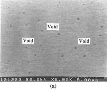
leading to the failure of dielectric strength; the small amount of Cu presented in the as-deposited sample was presumably due to the knock-on effect of ion bombardment during the SIMS profiling.17 The degradation of the breakdown field is generally believed to be correlated with Cu contamination in the dielectric layers, which may induce dielectric thinning18-20or result in increase of injection elec-tron currents,21-26thus leading to poor breakdown strength. Figure 5 illustrates the SEM micrographs showing the surface morphology of TaN/Cu/PAE-2/Si samples annealed at 200 and 4008C. A large num-ber of voids nonuniformly appeared on the topmost TaN surface (Fig. 5a), and the size of some voids enlarged as the annealing tem-perature was increased to 4008C (Fig. 5b). The results of electrical analyses indicated that the device failure was closely related to the formation of these voids.
TaN/Cu/(Ta, TaN)/PAE-2/Si capacitors.—Figure 6 illustrates the
distribution of breakdown field for the Cu-gate capacitors having a
Figure 2. Variations of (a) thickness, (b) percentage shrinkage of thickness,
and (c) refractive index of PAE-2 films annealed at various temperatures for 30 min in N2ambient.
S0013-4651(99)04-046-X CCC: $7.00 © The Electrochemical Society, Inc.
25 nm thick Ta as well as TaN diffusion barrier. Compared with the samples without diffusion barrier, significant improvement in ther-mal stability was obtained, apparently due to the barrier
effective-ness of Ta and TaN layers. In fact, it was reported that 25 nm thick Ta and TaN barriers in the structure of Cu/barrier/p1n junction diodes can sustain a 30 min thermal annealing up to 550 and 7508C, Figure 3. Breakdown field distributions of (a) TaN/Cu/PAE-2/Si and (b)
Al/PAE-2/Si capacitors annealed at various temperatures.
respectively, without causing degradation to the devices’ electrical characteristics.10Thus, the premature degradation at 4508C for the TaN/Cu/Ta/PAE-2/Si MIS capacitor is believed to be associated with the thermal instability of the complex Ta/PAE-2 system. Figure 7
shows the SIMS depth profiles for the as-deposited as well as 4508C annealed TaN/Cu/Ta/PAE-2/Si capacitors. It can be seen that a sub-stantial amount of Cu had permeated into PAE-2 (Fig. 7b). On the other hand, the SIMS depth profiles for the TaN/Cu/TaN/PAE-2/Si
Figure 6. Breakdown field distributions of (a) TaN/Cu/Ta/PAE-2/Si and (b) TaN/Cu/TaN/PAE-2/Si capacitors annealed at various temperatures. Figure 5. Top-view SEM micrographs showing the surface morphology of TaN/Cu/PAE-2/Si samples annealed at (a) 200 and (b) 4008C.
S0013-4651(99)04-046-X CCC: $7.00 © The Electrochemical Society, Inc. samples annealed at the same temperature show much less
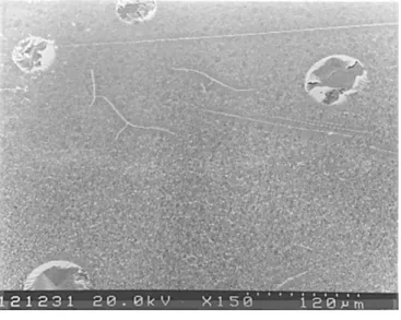
perme-ation of Cu into PAE-2 (not shown). Figure 8 illustrates the scanning electron microscopy (SEM) micrographs showing the surface mor-phology of TaN/Cu/(Ta, TaN)/PAE-2/Si samples annealed at 4508C. Many voids were found on the surface of the TaN/Cu/Ta/PAE-2/Si sample, while few were found on the sample of TaN/Cu/TaN/PAE-2/Si. The temperatures at which these voids appeared coincided with the temperature of electrical degradations; similar coincidence was also observed for the samples without barrier layers, as shown in Fig. 5. Since device failure is closely related to the formation of the voids, one can infer that electrical degradation occurred in the TaN/Cu/Ta/PAE-2/Si sample annealed at 4508C. Figure 9 illustrates the SEM micrographs showing the surface morphology of TaN/PAE-2/Si and Ta/PAE-TaN/PAE-2/Si samples annealed at 4508C. The surface mor-phology of the TaN/PAE-2/Si sample remained stable after anneal-ing at 4508C (Fig. 9a). However, blister- and/or knob-like artifacts were observed on the Ta surface for the 4508C annealed Ta/PAE-2/Si sample (Fig. 9b and c). We have found that the structure of Cu/(Ta, TaN)/SiO2/Si was able to remain intact at temperatures up to at least 4508C, as confirmed by the results of breakdown field measurements shown in Fig. 10, indicating the superior stability of the (Ta, TaN)/SiO2 system. There were reports that the blistering effect resulted in enhanced void formation in Al metal lines;27-29to the contrary, however, these local defects provided shortcuts for Cu per-meation, leading to dielectric degradation.
TDS analysis.—To clarify this observed phenomenon, we
pro-pose a failure mechanism regarding the outgassing behavior of PAE-2 with respect to the strength of the adhesive force between the bar-rier and PAE-2. An interfacial pressure-cooking state under the Ta layer may be produced by a gaseous pressure originating from the massive outgassing of PAE-2 at 4508C, as confirmed from the meas-ured TDS spectra shown in Fig. 11, wherein the primary peaks ob-served are H2O with a major mass peak at 18 and H2with a major mass peak at 2. Small mass peaks were also observed at 28, 44, and 76. It can be seen from Fig. 11 that the desorption occurred at a temperature as low as 1508C and increased drastically at temperatures above 4508C. It should be noted that the desorption of water (H2O) predominated among the outgassing species during the entire measurement period. The TDS measurement was conducted dynamically with a heating rate of 108C/min except that the temperature of 420 as well as 5008C was held constant for 10 min each. Thus, the extent of outgassing should be more serious for the samples of PAE-2 MIS capacitor ther-mally annealed at 4508C for 30 min. The early deterioration of the barrier layer would occur provided the outgassing-induced gaseous pressure exceeded the yielding strength of the barrier layer. Because
Figure 7. SIMS depth profiles of TaN/Cu/Ta/PAE-2/Si capacitor (a)
as-deposited and (b) 4508C annealed.
Figure 8. Top-view SEM micrographs showing the surface morphology of
(a) TaN/Cu/Ta/PAE-2/Si and (b) TaN/Cu/TaN/PAE-2/Si samples annealed at 4508C.
(a)
the upward gaseous stress forced the Ta film to deform downward and finally ruptured the surface, as shown in Fig. 9d, the impact that the gaseous pressure might have on the MIS sample studied may be gov-erned by the adhesive force between the overlying barrier layer (Ta or TaN) and the underlying dielectric (i.e., PAE-2). This inference was supported by the result of a pull test, which indicated that the adhesion between the TaN film and PAE-2 layer is much better than that between the Ta film and PAE-2 layer (average strength: 19.7 vs. 1.2 MPa). Thus, the result of electrical measurements that show the barrier capability of TaN films superior to that of Ta films is in com-plete accord with a stronger adhesive force between TaN and PAE-2 than that between Ta and PAE-2.
It was reported that the thermal stress induced from the mismatch of the thermal expansion coefficient caused voiding in metal lines and cracking in dielectric films.13,14,27,28The thermal stress cannot be ruled out from the possible cause of enhanced blister formation; however, further evidence is needed to confirm this point. This work
investigates, in particular, a new mechanism of gaseous stress-induced voiding enhanced by massive outgassing of PAE-2 layer due to its low glass transition temperature (,2908C).30
Conclusion
Copper penetrates readily into PAE-2 dielectric and degrades its dielectric strength in the MIS capacitor of Cu/PAE-2/Si structure at temperatures as low as 2008C. We found that thin Ta and TaN films of 25 nm thickness are qualified to be effective barriers against Cu penetration at temperatures up to 400 and 4508C, respectively. Specifically, the TaN barrier is superior to the Ta barrier because of its resistance to outgassing-induced gaseous stress of PAE-2, which is believed to arise from stronger adhesion of TaN to PAE-2 than that of Ta to PAE-2, thus leading to better long-term reliability.
Acknowledgments
The authors give their gratitude to Tong-Hsin Lee of USIC, Mong-Hsing Chuang, Jia-Chian Tsai, and Yu-Long Chin, as well as
Figure 9. SEM micrographs of 4508C annealed (a) TaN/PAE-2/Si (top view), (b) and (c) Ta/PAE-2/Si (top view), and (d) Ta/PAE-2/Si (oblique view). The
micrographs show blisters and knobs on the Ta surfaces.
(c)
(d)
(b)
(a)
S0013-4651(99)04-046-X CCC: $7.00 © The Electrochemical Society, Inc.
Yueh-Chiou Lin of TSMC and Chi-Ning Wang for their helpful tech-nical assistance and suggestions. This work was supported by the
National Science Council (ROC) under contract no. NSC 87-2215-E009-072.
Figure 10. Breakdown field distributions of (a) TaN/Cu/Ta/SiO2/Si and (b) TaN/Cu/TaN/SiO2/Si capacitors annealed at various temperatures.
The National Chiao-Tung University assisted in meeting the publication costs of this article.
References
1. M. T. Bohr, Tech. Dig. Int. Electron Devices Meet., 241 (1995). 2. X. W. Lin and D. Pramanik, Solid-State Technol., 63 (Oct 1998). 3. M.-A. Nicolet, Thin Solid Films, 54, 415 (1978).
4. M. Wittmer, J. Vac. Sci. Technol., A2, 273 (1984).
5. H. Ono, T. Nakano, and T. Ohta, Appl. Phys. Lett., 64, 1511 (1994). 6. P. Singer, Semicond. Int., 91 (June 1998).
7. B. Chin, P. Ding, B. Sun, T. Chiang, D. Angelo, I. Hashim, Z. Xu, S. Edelstein, and F. Chen, Solid-State Technol., 141 (July 1998).
8. X. Sun, E. Kolawa, J. S. Chen, J. S. Reid, and M. A. Nicolet, Thin Solid Films, 236, 347 (1993).
9. K. Holloway and P. M. Fryer, Appl. Phys. Lett., 57, 1736 (1990).
10. M. T. Wang, Y. C. Lin, and M. C. Chen, J. Electrochem. Soc., 145, 2538 (1998). 11. Y. C. Lin, M.S. Thesis, National Chiao-Tung University, Hsinchu, Taiwan (1997). 12. J. C. Chang, M.S. Thesis, National Chiao-Tung University, Hsinchu, Taiwan
(1996).
13. S. P. Jeng, M. C. Chang, L. Ting, K. Taylor, C. Lee, P. Mcanally, and R. H. Have-mann, 1995 International Symposium on VLSI Technology, Systems, and Applica-tions Conference Proceedings, p. 164 (1995).
14. C. Chiang, A. S. Mack, C. Pan, and D. B. Fraser, 1997 International Symposium on VLSI Technology, Systems, and Applications Conference Proceedings, p. 37 (1997).
15. R. N. Vrtis, K. A. Heap, W. F. Burgoyne, and L. M. Robeson, Mater. Res. Soc. Symp. Proc., 443, 171 (1997).
16. T. T. Wu, M.S. Thesis, National Chiao-Tung University, Hsinchu, Taiwan (1996). 17. P. Bai, G. R. Yang, L. You, T. M. Lu, and D. B. Knorr, J. Mater. Res., 5, 989 (1990). 18. K. Honda, A. Ohsawa, and N. Toyokura, Appl. Phys. Lett., 45, 270 (1984). 19. G. Raghavan, C. Chiang, P. B. Anders, S. M. Tzeng, R. Villasol, G. Bai, M. Bohr,
and D. B. Fraser, Thin Solid Films, 262, 168 (1995).
20. C. Chiang, S. M. Tzeng, G. Raghavan, R. Villasol, G. Bai, M. Bohr, H. Fujimoto, and D. B. Fraser, 1994 VMIC Conference Proceeding, p. 414 (1994).
21. K. I. Takeda, K. Hinode, I. Oodake, N. Oohashi, and H. Yamaguchi, 1998 IEEE IRPS Conference Proceeding, p. 36 (1998).
22. A. L. S. Loke, C. Ryu, C. P. Yue, J. S. H. Cho, and S. S. Wong, IEEE Electron Device Lett., EDL -17, 549 (1996).
23. A. L. S. Loke, J. T. Wetzel, C. Ryu, W. J. Lee, and S. S. Wong, Symp. VLSI Tech-nol. Tech. Dig., 26 (1998).
24. H. Miyazaki, K. Hinode, Y. Homma, and N. Kobayashi, Jpn. J. Appl. Phys., 35, 1685 (1996).
25. M. Vogt, M. Kachel, K. Melzer, and K. Drescher, Microelectron. Eng., 33, 349 (1997).
26. H. Miyazaki, H. Kojima, and K. Hinode, J. Appl. Phys., 81, 7746 (1997). 27. D. Pramanik, Solid-State Technol., 69 (Sept 1995).
28. N. Hirashita, I. Aikawa, T. Ajioka, M. Kobayakawa, F. Yokoyama, and Y. Sakaya, 1990 IEEE IRPS Conference Proceeding, p. 216 (1990).
29. H. G. Tompkins and C. Tracy, J. Electrochem. Soc., 136, 2331 (1989). 30. N. P. Hacker, MRS. Bull., 22, 36 (1997).