Effect of the inclusion of small metallic components in a two-dimensional dielectric photonic
crystal with large full band gap
Chien C. Chang,1 J. Y. Chi,2R. L. Chern,1 C. Chung Chang,1C. H. Lin,2and C. O. Chang1 1Institute of Applied Mechanics, National Taiwan University, Taipei 106, Taiwan, Republic of China
2Opto-Electronics & Systems Laboratories, Industrial Technology Research Institute, Hsinchu 310, Taiwan, Republic of China (Received 9 October 2003; revised manuscript received 1 March 2004; published 24 August 2004)
In this study, we investigate the effect of metallic inclusion modeled as perfect conductor on a dielectric photonic crystal(silicon/air) with large full band gap. The dielectric crystal consists of a hexagonal array of circular dielectric columns, each connected to its nearest neighbors by slender rectangular rods. It is found that inclusion of small metallic components inside the circular dielectrics sharply “turns off“ the full band gap of the dielectric photonic crystal. By increasing the radius of metallic inclusion above a threshold value, the full band gap(of the metallodielectric photonic crystal) makes its appearance again and continues to grow in size. On the other hand, metallic inclusion in the air region shows an opposite trend that the full band gap is not turned off, and its size diminishes gradually to zero with increasing the radius of inclusion. These peculiar behaviors can be explained on a unified basis by examining different types of boundary conditions for TM and TE modes, and employing variational arguments based on Rayleigh’s quotients. Moreover, the free-electron model for metallic components is also considered for TM modes. At large plasma frequencies, these modes show very close band structures to those described above for the case of perfect conductors.
DOI: 10.1103/PhysRevB.70.075108 PACS number(s): 78.20.Bh, 42.70.Qs, 02.70.Bf
I. INTRODUCTION
Photonic crystals are also known as photonic band-gap materials. The most attractive/distinguished feature of photo-nic crystals is their full band-gap structures.1,2 Large full band gaps allow strong photon localization with the gap,3,4 and a detailed manipulation of photonic defect states.5,6 In-tensive studies have been mainly concerned with dielectric materials. They have important applications such as microcavities,7optical waveguides,8defect mode lasers,9 op-tical fibers10and feedback mirror in laser diodes.11Recently, photonic crystals comprising metal or metallodielectric ma-terials have become increasingly important.
Photonic crystals with metallic components can possess much larger band gaps.12–15 They may also act like nearly perfect reflectors.16,17 New applications include high-impedance surfaces18 and resonator gyrotron.19 In addition, new electromagnetic phenomena are explored in metallic crystals such as a new forbidden band,20 band gaps in the visible range,21 strong capacitive coupling,22 extraordinary optical transmission,23extremely low frequency plasmons,24 surface enhanced Raman scattering25 and a perfect lens.26 Previous studies have shown that by including metallic com-ponents in the dielectric region the band gap can be signifi-cantly opened up or enlarged in three dimensions.13,27 How-ever, there are also disadvantages of using metals as they are usually quite lossy at optical frequencies.20
In the literature, there are three ways to model the metal property. The first one is to assume metals to be perfect con-ductors. The second one is to model metals as dispersive materials with the simple free-electron form of dielectric function. The third one is to model metals as dissipative materials with the Drude type of dielectric function. There-fore, metallodielectric photonic crystals could be modeled as combined structures of dielectric materials with one of the three types of metallic materials. In the present study,
metal-lic components in photonic crystals are modeled as the per-fect conductors. Moreover, we also consider dispersive me-tallic components with free-electron model for TM modes(E polarization). Compared to the dielectric counterpart, com-putation of photonic band structures for metallic or metall-odielectric photonic crystals is more difficult. Below the plasma frequency, metals are able to reflect most of the elec-tromagnetic radiations, and very little fields could sustain inside. Therefore, the electromagnetic field is compressed in the dielectric region, and may vary drastically in the case of large portion of metallic inclusion. This becomes even more severe for TE modes (H polarization), which intrinsically possess more irregular patterns. The computed eigenfunc-tions are more difficult to converge, especially at very long wavelengths.28 In order to resolve the more complex struc-tures of eigenfunctions, higher resolution and more efficient methods are necessary.
There are several approaches to the band structure com-putation of metallic and metallodielectric photonic crystals. The most widely used method for this purpose is plane wave expansion.16,29–31Other various techniques include the trans-fer matrix method,32 the finite-difference time-domain method,13,33–35finite difference method,17,28generalized Ray-leigh identity method,36the multiple multipole method37and the so-called order-N method.38 In our previous paper, a highly fast and accurate inverse method with multigrid ac-celeration is developed to be applicable to photonic crystals comprising dielectric materials of arbitrary shape.39The de-veloped algorithm is capable of resolving multieigenvalue band structures, and is applicable to photonic crystals with interfaces of strong contrast. In this study, we extend this method to be applicable to metallodielectric photonic crys-tals which contain both dielectric and perfectly conducting materials. The field inside the perfect conductor may be taken to be identically zero. Therefore, internal boundary conditions must be imposed on the conducting surfaces. The
eigensystem of the band structure remains a standard eigen-value problem, as is the case of dielectric photonic crystals. Furthermore, the eigensystem preserves the Hermitian prop-erty and has real eigenfrequencies.
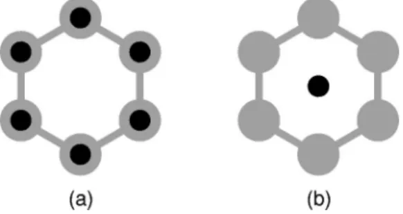
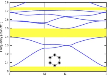
In the present study we are focused on the effect of me-tallic inclusion on band structures of dielectric photonic crys-tals. We start by considering a dielectric crystal(with lattice constant a) as the base structure, as shown in Fig. 1. The crystal consists of a hexagonal array of circular dielectric columns of radius r, each connected to its nearest neighbors by slender rectangular rods of width d.39 The reason of choosing this geometry is as follows: previous studies indi-cate that band gaps for E polarization are favored in a lattice of isolated high- region, and band gaps for H polarization are favored in a connected lattice.3 A compromise must therefore be reached between the sizes of the dielectric col-umns and the connecting rods in order to obtain an optimal full band gap. In fact, Fig. 2 shows that the optimal (and maximum) full band gap is attained when the band gaps for TM and TE modes have the simultaneous band gap, or the same band edges.40
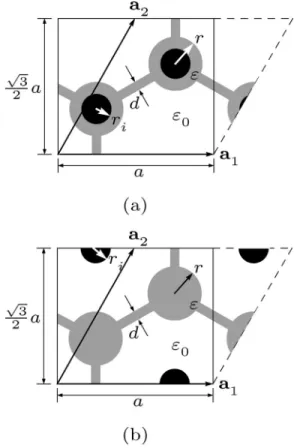
Next, we consider circular columns of perfectly conduct-ing material embedded inside the dielectric columns [Fig.
3(a)], or in the air region [Fig. 3(b)], to study the effect of metallic inclusion. The findings are several. The inclusion of metallic components in the dielectric region sharply “turns off” the full band gap of the dielectric photonic crystal, no matter how small is the size of the inclusion. The small size of metallic inclusion is advantageous for higher operating frequencies as the lossy effect will also be small. The band structure remains in the “off” state until the radius of inclu-sion reaches a threshold value. By increasing the radius of the metallic inclusion above the threshold value, the full band gap(of the metallodielectric photonic crystal) makes its appearance again. After that, the size of the full band gap increases monotonically with further increasing the radius of metallic inclusion. The latter result is consistent with early observations by other authors.15,28 On the other hand, the inclusion of perfectly conducting materials in the air region does not “turn off” the full band gap of the dielectric photo-nic crystal. In this case the size of the full band gap decreases monotonically as the radius of inclusion is increased. All these peculiar behaviors can be explained on a unified basis by examining different types of boundary conditions im-posed on TM and TE modes on the metal surfaces and employing variational arguments based on Rayleigh’s quo-tients. Finally, interesting comparisons for the TM modes are made with the free-electron model for the metallic compo-nents at different plasma frequencies in the mode shapes and band structures.
II. BASIC EQUATIONS AND NUMERICAL METHODS For linear isotropic and frequency-independent dielectric materials with permeability close to one, the time-harmonic modes in two dimensions for E polarization (TM) can be written as −
冉
2 x2+ 2 y2冊
E =冉
c冊
2 E, 共1兲and H polarization(TE) as −
冋
x冉
1 x冊
+ y冉
1 y冊
册
H =冉
c冊
2 H, 共2兲where E = Ez and H = Hz are the electric and magnetic field intensities, respectively, and =共r兲 is the dielectric func-tion. To discretize Eqs. (1) and (2), a second order central
FIG. 1. Dielectric photonic crystal(silicon-air) consisting of a hexagonal array of circular cylinders, each connected to its nearest neighbors by slender rectangular rods.
FIG. 2. (Color online) Band structure computed with a 256
⫻256 grid for the dielectric photonic crystal in Fig. 1 with r/a
= 0.155 and d / a = 0.035 for/0= 13.
FIG. 3. Metallodielectric photonic crystal with metallic circular columns embedded(a) inside the dielectric columns (b) in the air
finite difference scheme is used. Inside the perfect conductor, the electric field E vanishes, and the magnetic field H may be taken to be zero. The boundary condition on the perfectly conducting surface for E and H polarizations are, respectively,
E = 0 and H
n = 0, 共3兲
where /n is the normal derivative at a point on
the surface.41 In the present study, we also consider the dispersive free-electron model for the metallic components,
共兲 = 1 −p 2
2, 共4兲
wherepis the plasma frequency. In particular, we compute the band structures for E polarization. The eigenvalue prob-lem outside the metallic region is described by Eq.(1) while inside the metallic region it can be recast to the following form:
冋
−冉
2 x2+ 2 y2冊
+冉
p c冊
2册
E =冉
c冊
2 E. 共5兲For periodic structures, the domain of computation can be chosen as one unit cell along with suitable boundary condi-tions. For convenience of finite difference formulation, the domain of computation is chosen as a rectangle with the same area of the primitive cell of the hexagonal lattice as
shown in Fig. 4. Bloch’s theorem is applied at the domain boundary:
Ek共r + ai兲 = eik·aiEk共r兲, 共6兲
Hk共r + ai兲 = eik·aiHk共r兲, 共7兲
where Ekand Hkare the Bloch functions for the electric and
magnetic fields, respectively, associated with the wave vector
k in the first Brillouin zone, and ai共i=1,2兲 is the lattice
translation vector. For the hexagonal lattice, a1= a共1,0兲 and
a2= a共1/2,
冑
3 / 2兲. Since a2 makes 60 degrees with the x-axis, the application of Bloch’s condition in the y-direction should be additionally accompanied by one half cell in thex-direction.
From the practical point of view, the first few branches of eigenvalues are of primary interest. As a first step, it is natural for us to propose the method of inverse iteration42,43to compute the eigenvalues as well as eigenvec-tors from the smallest one. Let A be the discretization matrix of the differential operators in Eq. (1) or (2) or (5). The method of inverse iteration is based on the following equations:
共A −I兲x = v. 共8兲
The basic idea is to chooseclose to the smallest eigenvalue one wishes to compute and do the following steps.
(1) Compute the first eigenpair: (a) Pick up a random vector as the initial v. (b) Solve Eq. (8) for x and replace
v by the normalized x. (c) Repeat step (b) until 储Av−v储2⬍⑀, where⑀is a small number. The eigenvalue is obtained by the Rayleigh quotient具v,Av典. The first eigenpair is denoted by共1, q1兲.
(2) Compute the second eigenpair: (a) Pick up a random vector as the initial v.(b) Solve Eq. (8) for x and deflate the components of x in the direction of the first eigenvector q1 by
x← x − 具q1,x典q1. 共9兲 Replace v by the normalized x. 共c兲 Repeat step 共b兲 until 储Av−v储2⬍⑀, where⑀is a small number. The eigenvalue is obtained by the Rayleigh quotient具v,Av典. The second eigen-pair is denoted by共2, q2兲.
(3) Compute the nth eigenpair: (a) Pick up a random vec-tor as the initial v. (b) Solve Eq. (8) for x and deflate the components of x in the directions of the first n − 1 eigenvec-tors q1. . . qn−1by
x← x −
兺
k=1 n−1
具qk,x典qk. 共10兲 Replace v by the normalized x. 共c兲 Repeat step 共b兲 until 储Av−v储2⬍⑀, where⑀is a small number. The eigenvalue is obtained by the Rayleigh quotient具v,Av典. The nth eigenpair is denoted by共n, qn兲.
The algorithm of inverse iteration is designed as follows:
FIG. 4. Domain of computation for the metallodielectric photo-nic crystal with metallic circular columns embedded(a) inside the dielectric columns(b) in the air region.
InverseEigen { for n = 1 to S
Initial guess v
do
Solve 共A−I兲x=v by LUD or PCG
Deflate x by q1to qn−1 Set v = x /储x储
Rayleigh Quotient n=具v,Av典
until储共A−nI兲v储2⬍⑀ Set qn= v
end }
where1艋2艋¯ 艋S is the sequence of smallest eigen-values, and q1. . . qS are the corresponding eigenvectors. The inner product具·,·典 is defined as
具x,y典 =
兺
iwi¯xiyi, wi=
再
共ri兲, for E polarization; 1, for H polarization in view of the different orthogonal properties of the E field and the H field:
1
Vcell
冕
Vcell共r兲Em*共r兲E n共r兲dr =␦mn, 共11兲 1 Vcell
冕
VcellHm *共r兲H n共r兲dr =␦mn, 共12兲 where En and Hn are the nth eigenfunctions of the electric and magnetic fields, respectively. Vcelldenotes the volume of the primitive cell and␦mn is the Kronecker delta. LUD de-notes the LU decomposition solver for matrix inversion, andPCG the preconditioned conjugate gradient solver.
In the previous study, we proposed an idea to accelerate the convergence of matrix inversion in the algorithm. The idea is to embed inverse iteration in the multigrid accelera-tion structure. The basic idea of the multigrid method44,45is to solve the matrix problem by approximating the solution on a fine grid, solving the residue on a coarse grid, and then improving the solution on the fine grid. Successively apply-ing this idea on multilevel of grids causes a relaxation of errors on different resolution, and hence accelerates the con-vergence of inverse iteration.
Let there be L levels of grids. On each grid level m, the differential operator is discretized to form the matrix A共m兲. The inverse method with multigrid acceleration is imple-mented by the following steps.
(1) Given random vectors as the initial guesses, compute the first n eigenpairs共1共1兲, q1共1兲兲...共n共1兲, qn共1兲兲 on the coarsest grid level by the inverse algorithm described previously.
(2) Interpolate q1
共1兲. . . q
n
共1兲 to the next finer grid level as
the initial guesses. Replace LUD in the inverse algorithm by the multigrid V-cycle solver,44,45 and compute the first n eigenpairs共1共2兲, q1共2兲兲...共n共2兲, qn共2兲兲 on this grid level.
(3) Repeat step (2) until the eigenpairs on the finest grid level are obtained.
The algorithm of multilevel inverse iteration is designed as follows: FMGInverse { Call InverseEigen at m = 1 for m = 2 to L for n = 1 to S Interpolate qn共m−1兲to v共m兲 do Solve共A共m兲−I兲x共m兲= v共m兲by MGV Deflate x共m兲by q1共m兲to qn−1共m兲 Set v共m兲= x共m兲/储x共m兲储 Rayleigh Quotientn共m兲=具v共m兲, A共m兲v共m兲典 until储共A共m兲−n共m兲I兲v共m兲储2⬍⑀ Set qn共m兲= v共m兲 end end}
Notice that in the above algorithm, the Rayleigh quotient is
TABLE I. Computing times in CPU seconds for the first six eigenmodes at point K for the metallodielectric photonic crystal in Fig. 3(a) with different ri/ a.
Ngrid No metals ri/ a = 0.01 ri/ a = 0.02 ri/ a = 0.05 64⫻64 0.203 0.297 0.297 0.438 128⫻128 0.937 1.391 1.25 1.422 256⫻256 3.844 6.922 7.672 6.844 512⫻512 12.828 42.125 27.359 32.422 1024⫻1024 39.641 179.187 108.171 155.125
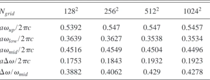
TABLE II. Convergence test for the full band gap against the grid size for the metallodielectric photonic crystal in Fig. 3(a) with ri/ a = 0.1. Ngrid 1282 2562 5122 10242 aup/ 2c 0.5392 0.547 0.547 0.5457 alow/ 2c 0.3639 0.3627 0.3538 0.3534 amid/ 2c 0.4516 0.4549 0.4504 0.4496 a⌬/2c 0.1753 0.1843 0.1932 0.1923 ⌬/mid 0.3882 0.4062 0.429 0.4278
FIG. 5.(Color online) Computing times in CPU seconds for the first six eigenmodes at point K for the metallodielectric photonic crystal in Fig. 3(a) with different ri/ a.
updated after each multigrid V-cycle solver which may pro-vide only an approximate solution to the inverse equation. As a result, the Rayleigh quotient updates more frequently and converges faster to the eigenvalue. The whole idea of pro-posing an inverse method with multigrid acceleration for computing photonic band structures has now become clear. First of all, the boundary condition(3) is used to take care of perfectly conducting inclusions. Second, the deflation in the algorithm of inverse iteration enables singling out the eigen-values one by one from the smallest even when they may be degenerate. Third, interlacing the inverse iteration and mul-tigrid acceleration makes the whole method an amazingly fast algorithm for computing photonic band structures, as demonstrated below.
III. RESULTS AND DISCUSSION
In this study, we consider the dielectric crystal in Fig. 1 as the base structure with fixed r / a = 0.155 and d / a = 0.035 for /0= 13. As an example of the test, we compute the first six
frequency bands at point K for the metallodielectric photonic crystal by embedding circular columns of perfect conductors in the base structure. Table I lists the computing times in central processing unit (CPU) seconds for different radii of metallic inclusion. The computations are performed on a Pentium 4 - 2.8 GHz PC. Figure 5 shows a plot of these com-puting times, which demonstrates that the present method is of good order N = Ngrid.
The convergence of the computed results against the grid size is illustrated by computations performed on four differ-ent grids: 1282, 2562, 5122, and 10242. Table II lists the re-sults of the band edges(up,low), midgap frequency共mid兲, band width 共⌬兲 and gap-midgap ratio 共⌬/mid兲 for the metallodielectric photonic crystal in Fig. 3(a) with ri/ a = 0.1 for the grid Ngrid艌128⫻128. It can be seen that the numeri-cal results for different grids fluctuate mildly but are in gen-erally good agreement with each other. In the present study, the grid size Ngrid= 256⫻256 will be used in most computa-tions.
Let us now start to study the effect of metallic inclusion shown in Fig. 3(a) by increasing the radius of inclusion ri/ a.
FIG. 6. (Color online) Band structure computed with a 256
⫻256 grid for the metallodielectric photonic crystal in Fig. 3(a)
with ri/ a = 0.01.
FIG. 7. (Color online) Band structure computed with a 256
⫻256 grid for the metallodielectric photonic crystal in Fig. 3(a)
with ri/ a = 0.06.
FIG. 8. (Color online) Band structure computed with a 256
⫻256 grid for the metallodielectric photonic crystal in Fig. 3(a)
with ri/ a = 0.1.
FIG. 9. (Color online) Band structure computed with a 256
⫻256 grid for the metallodielectric photonic crystal in Fig. 3(a)
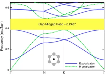
Figures 6–9 present the band structures computed with a 256⫻256 grid, respectively, for ri/ a = 0.01, 0.06, 0.1 and 0.2. At the small ri/ a = 0.01, there is no longer a full band gap, and for which we say that the metallic inclusion sharply “turns off” the full band gap of the dielectric photonic crys-tal. In a comparison of Fig. 6 with Fig. 2, we observe that the first two branches of TM modes suddenly shift upward, tres-passing into the region of the original full band gap, blocking it completely. The TE modes are relatively inactive to metal inclusion, and the band structure almost remains unchanged. The trend of the upward shift of TM modes continues. As
ri/ a is increased to about 0.06 (Fig. 7), the full band gap remains in the “off” state. However, the lower edge of the first TM branch is about to move away from the upper edge of the first TE branch. Meanwhile, the band gap of the TE modes is widening in size. After this threshold value共ri/ a = 0.06兲, the full band gap makes its appearance again, soon becoming widely open as the radius ri/ a is further increased. At ri/ a = 0.1, the lower edge of the first TM branch ap-proaches the upper edge of the widely opened band gap of the TE modes. At even larger ri/ a, the upward-shifted TM modes have moved completely out of the region of TE band gap, leaving the full band gap size to be solely determined by the TE modes. In the meantime, the first few branches of TM modes are flattening out with the group velocity almost iden-tically zero(Fig. 9). These phenomena demonstrate that the metallodielectric photonic crystals behave more like metallic photonic crystals at large ri/ a. This can be reasonably ex-pected because at ri/ a = 0.155 the metal inclusions have al-ready replaced in full the circular dielectric columns 共r/a = 0.155兲. As the metallic components become large enough, the eigenfrequencies of TM modes tend to be flattened out.36 Eventually these TM modes become standing waves with no dispersion. In the limiting case when the conducting materi-als connect to each other, both TM and TE band structures are straight lines.30This is a typical behavior of the resonant modes of cavity.46 They are standing waves confined and resonant in the dielectric region with eigenfrequencies inde-pendent of the wave vectors. The propagation of electronetic waves is shielded and neither electric field nor mag-netic field could penetrate the conducting materials.
The behaviors observed may be explained by considering the different types of boundary conditions in(3) for TM and TE modes, and employing the variational argument based on the Rayleigh quotients:
QTM= bVcell兩ⵜE兩2d bVcell兩E兩2d , 共13兲 QTE= bVcell 1 兩ⵜH兩 2d bVcell兩H兩 2d , 共14兲
respectively, for TM and TE modes, where we recall that
Vcelldenotes the volume of the primitive cell. The inclusion of metallic materials significantly modifies the band structure of TM modes by introducing a zeroth-order band gap,28 which is analogous to the cutoff behavior of conventional
waveguides. However, the origin of the cutoff behavior for the TM modes of the metallodielectric photonic crystal is very different from that of the conventional waveguide. In the conventional waveguide, the cutoff frequency originates from the sustenance of transverse oscillations,46while in the metallodielectric photonic crystals, the electric fields are identically zero inside and on the surface of the perfect con-ductors. In particular, consider the TM modes at the symmet-ric point⌫. If the zero-frequency solution (without a cutoff frequency) is allowed in the crystal, the electric field should be constant everywhere outside the perfect conductors. By the continuity of the electric field at the metal boundary共E = 0兲, this constant must be zero, resulting in a trivial solution. Therefore, TM modes with zero frequency do not exist, mak-ing an appearance of the cutoff frequency. On the other hand, the cutoff behavior is not observed in TE modes for metall-odielectric crystals. This is because constant solutions with zero frequency are allowed in the crystal without violating the boundary condition共H /n = 0兲 for TE modes.
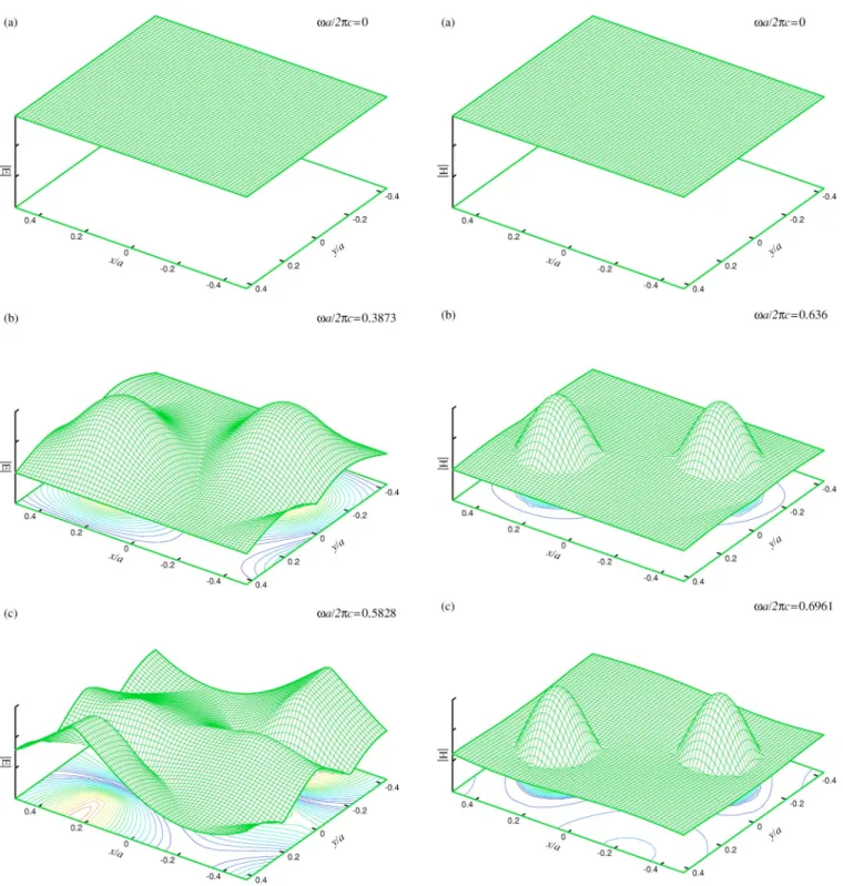
The variational analysis based on (13) and (14) argues that both TM and TE modes favor accommodation of their eigenfunctions in high- regions in order to minimize the Rayleigh’s quotients. However, because of the different boundary conditions, the inclusion of metallic components repels the eigenfunctions of TM modes outward from the inclusion more effectively than those of TE modes. In the first place, we consider the dielectric photonic crystal in Fig. 1 and plot the first three eigenfunctions in magnitude at point ⌫ for TM modes in Fig. 10 and for TE modes in Fig. 11. Since there are no internal boundary conditions, both modes allow zero-frequency eigenfunctions. As expected, all the eigenfunctions except the zero-frequency ones are concen-trated on and around the higher- circular regions, but the TM eigenfunctions are more spread out. For a strong con-trast, we next consider the metallodielectric photonic crystal in Fig. 3(a) with ri/ a = 0.02 and plot the first three eigenfunc-tions in magnitude at point⌫ for TM modes in Fig. 12 and for TE modes in Fig. 13. For TM modes, the argument based on the boundary condition has excluded the possibility of constant eigenfunctions. All the three eigenfunctions rise sharply from 0 at the metal surface to peak values, causing large gradients in the eigenfunctions and thus contributing to the sudden upshift of the eigenvalues. On the other hand, the boundary condition for TE modes does allow constant eigen-functions, and only requires at the metal surface a round shape of the eigenfunctions around the rim of the metal in-clusion. This requirement does not change effectively the TE bands and the shapes of the corresponding eigenfunctions. There is one further comparison with the case of dielectric photonic crystals that for either TM or TE modes, the eigen-functions of the metallodielectric photonic crystals tend to be even more concentrated on and near the annular high- re-gions for better minimization of the Rayleigh’s quotients. This is no longer possible if the radius of metal inclusion
ri/ a comes close to that of the dielectric circular columns
r / a = 0.155. The eigenfunction of the first TM mode rises
more abruptly from 0, while the first TE mode can adjust itself to be an even smoother function.
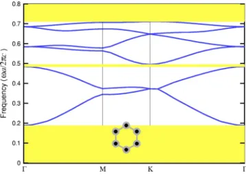
Figure 14 shows the gap map computed with a 128 ⫻128 grid for the metallodielectric photonic crystal in Fig.
3(a) by varying the radius ri/ a. As the shifted TM bands are trespassing into the original band gap region of the dielectric photonic crystals, the band structure remains in the “off” state. By increasing the size of the metallic inclusion above a threshold value, the full band gap (of the metallodielectric photonic crystals) opens again and its size continues to grow as the upward shifted TM bands are moving away from the upper band edge of the TE band gap. In this case, the thresh-old value of the metallic inclusion is about ri/ a = 0.06, and the corresponding band structure at this inclusion is shown in
Fig. 7. It is noticed that for large size of metallic inclusion, the full band gap is very large because the zeroth-order band gap for the TM mode covers the whole band gap for TE mode. This phenomenon was also identified in Ref. 28.
On the other hand, we consider metallic inclusions in the air region, as shown in Fig. 3(b). The full band gap decreases monotonically in size and finally diminishes to zero with increasing the radius ri/ a of metallic inclusion. Figure 15 shows the gap map computed with a 128⫻128 grid by vary-ing the radius ri/ a. It is observed that the cutoff behavior for
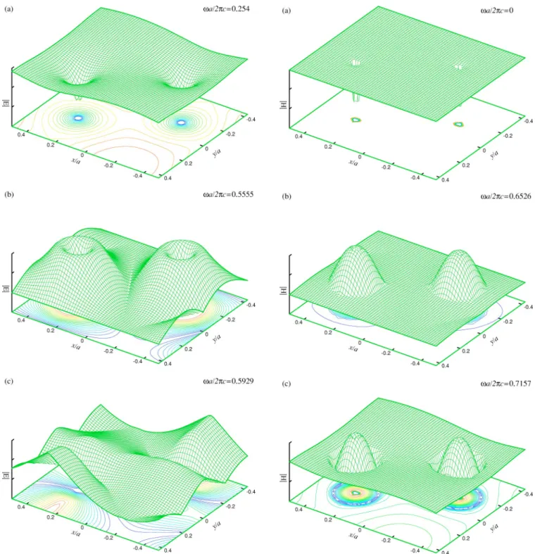
FIG. 10. (Color online) The first three TM eigenfunctions in magnitude at point⌫ for the dielectric photonic crystal in Fig. 1.
FIG. 11. (Color online) The first three TE eigenfunctions in magnitude at point⌫ for the dielectric photonic crystal in Fig. 1.
TM modes also exists, as in the case of metallic inclusion in the dielectric region. But the shifted TM bands do not tres-pass into the original band gap region of the dielectric pho-tonic crystal, and the band structure remains in the “on” state. In fact, only the first TM band in a portion near point⌫ is substantially shifted upward, while all the other higher bands are changed only slightly. The fields(TM and TE) in the air region are relatively weaker than in the dielectric region, and therefore the effect of metallic inclusion is
smaller. Meanwhile, the TE band gap begins to shrink and finally leads the full band gaps to close. Figure 16 shows the detailed band structure for the metallodielectric photonic crystal at ri/ a = 0.005. In comparison with Fig. 2, the band structure is almost identical to that for the dielectric crystal without metallic inclusion except the first TM band near point⌫. Figure 17 shows another band structure at the larger
ri/ a = 0.1. In this case, the band edges of the TE band gap
FIG. 12. (Color online) The first three TM eigenfunctions in
magnitude at point⌫ for the metallodielectric photonic crystal in Fig. 3(a) with ri/ a = 0.02.
FIG. 13. (Color online) The first three TE eigenfunctions in magnitude at point⌫ for the metallodielectric photonic crystal in Fig. 3(a) with ri/ a = 0.02.
become close to each other, making the full band gap smaller.
Next, as an intermediate structure, metallic components are only included in one of two dielectric circular columns for each primitive cell. It is expected that the band structure also behaves in an intermediate manner. This is indeed the case, as shown by the gap map in Fig. 18. The full band gap is not turned off upon inclusion of small metallic compo-nents, but is divided into two branches as ri/ a is increased to about 0.014. The upper branch diminishes to zero as ri/ a reaches 0.03, while the lower branch continues to grow gradually in size, which is however smaller than the case of double inclusion (cf. Fig. 14). These behaviors can also be explained as the result of the upward shift of the first two TM bands. As ri/ a is increased from 0, the upward shift is not strong enough to make the first TM band cross the band-gap region of TE modes, while the second TM band does trespass into the region. In trespassing, the second TM band, being narrower in size, does not completely block the band gap of the TE modes, leading to a division of the full band gap into two branches. As ri/ a is further increased, the upward shift of the second TM band eventually makes the upper branch disappear. At large ri/ a, the band structure is the balanced result of both effects of metallic and dielectric components.
Finally, we consider the free-electron model (4) for the metallic components and compute the band structures for E polarization. Figure 19 shows the second eigenfunction in magnitude at point ⌫ for TM modes for ri/ a = 0.02 at
pa / 2c = 1. The mode pattern is very similar to Fig. 12(b). It is noticed that the field inside the metal is not forced to zero and the boundary condition (3) is not applied on the metal surface. As a result, the field may somewhat penetrate into the metallic region and no sharp discontinuity exists in the interface. In spite of similarity in mode shapes, the band structures could be very different depending on the plasma frequency. In order to see a trend toward perfect conductors, band structures are presented for ri/ a = 0.01 at different plasma frequenciespa / 2c = 1, 4 and 8. At the lower value
pa / 2c = 1, Fig. 20 shows that the band structures are quite different from those presented for the case of perfect conduc-tors in two places:(i) the cutoff frequency of the first band is relatively small, and(ii) the band gap is wide-open between the second and third bands. At the medium valuepa / 2c = 4, Fig. 21 shows that the cutoff frequency becomes larger while the band gap between the second and the third bands
FIG. 14. A map of band gaps computed with a 128⫻128 grid for the metallodielectric photonic crystal in Fig. 3(a) by varying the radius ri/ a.
FIG. 15. A map of band gaps computed with a 128⫻128 grid for the metallodielectric photonic crystal in Fig. 3(b) by varying the radius ri/ a.
FIG. 16. (Color online) Band structure computed with a 256
⫻256 grid for the metallodielectric photonic crystal in Fig. 3(b)
with ri/ a = 0.005.
FIG. 17. (Color online) Band structure computed with a 256
⫻256 grid for the metallodielectric photonic crystal in Fig. 3(b)
becomes smaller. At the large value pa / 2c = 8, Fig. 22
shows that the cutoff frequency is even larger and has the value 0.188 which is pretty close to 0.211 in Fig. 6 for per-fect conductors, while the band gap between the second and the third bands is now very small. A close comparison be-tween Fig. 22(free-electron model) and Fig. 6 (perfect con-ductors) shows that the whole band structures for TM modes are in close agreement with each other. These trends are expected because as the plasma frequency becomes larger, the dielectric function becomes more negative. Equivalently, the index of refraction is purely imaginary and large in mag-nitude. The fields inside the metallic region are therefore evanescent modes. In the limit of perfect conductors, the evanescent field is completely expelled from the metal and vanishes there.
IV. CONCLUDING REMARKS
In this study, we have extended an inverse method with multigrid acceleration39 to compute the band structures of two-dimensional metallodielectric photonic crystals. The present article is focused on the effect of metallic inclusion
in a dielectric photonic crystal. The metallic components are first modeled as perfectly conducting materials. In particular, we consider two cases of inclusion: metals(i) inside dielec-tric circular columns, or(ii) in the air region of a hexagonal lattice made of silicon and air共/0= 13兲. The two types of inclusion have completely different effects on the band struc-tures and gaps. In the case(i), the full band gap is suddenly “turned off” upon metallic inclusion, remaining in the “off” state until the radius of inclusion reaches a threshold value, making its appearance again with further increasing the ra-dius, and eventually behaving like metallic photonic crystals. For the case(ii), the full band gap only changes slightly in size upon metallic inclusion, but gradually diminishes to zero with increasing the radius of inclusion. These different trends of behavior have been successfully explained on a unified basis by examining the different types of boundary condi-tions for TM and TE modes at metal surfaces, and employing a variational analysis based on Rayleigh’s quotients for the TM and TE modes. Moreover, intermediate dielectric photo-nic crystals are shown to exhibit intermediate behaviors in the band structures.
FIG. 18. A map of band gaps computed with a 128⫻128 grid for the intermediate metallodielectric photonic crystal by varying the radius ri/ a.
FIG. 19.(Color online) The second eigenfunction in magnitude at point⌫ for the metallodielectric photonic crystal (free-electron model) in Fig. 3(a) with ri/ a = 0.02 andpa / 2c=1.
FIG. 20. (Color online) A band structure computed with a 256
⫻256 grid for the metallodielectric photonic crystal (free-electron
model) in Fig. 3(a) with ri/ a = 0.01 andpa / 2c=1.
FIG. 21. (Color online) Band structure computed with a 256
⫻256 grid for the metallodielectric photonic crystal (free-electron
The perfectly conducting materials as metallic inclusion present an ideal case for studying the metallic shielding ef-fects on photonic structures. More real and complicated phe-nomena may resort to the study of dispersive, and even dis-sipative effects of metallic materials. In this study, we also consider the dispersive free-electron model and compute the band structures for the modes of E polarization. The numeri-cal results are presented at different plasma frequencies
pa / 2c. It is shown that aspa / 2c becomes large, these modes show close similarity to those computed for the me-tallic components modeled as perfect conductors. However, the present method cannot be applied straightforwardly to compute band structures of H polarization. On one hand, computation of the band structures of H polarization cannot be obviously recast to a standard eigenvalue problem: the eigenfunctions no longer constitute an orthogonal family in
the ordinary sense. On the other hand, computation of the modes of H polarization is further complicated by the exis-tence of resonant modes near the surface plasmon frequency. This special feature associated only with the H polarization has been studied using finite-difference time-domain method34 and multiple multipole method.37 The latter refer-ence might suggest that in the present formulation the eigen-value problem of the H polarization could be attacked by the technique of detection used in nonlinear eigenvalue prob-lems. For dissipative metallic materials, both the dielectric function and eigenfrequencies become complex. In addition to the plasma frequency, the relaxation time of the free elec-tron may also play important roles on the dispersion relations of metallic photonic crystals (cf. Refs. 34 and 37). These more challenging topics are currently being under investiga-tion, and the results will be reported elsewhere.
Finally, some comments are available for possible fabri-cation of the proposed metallodielectric photonic crystals. The following procedures of microelectronics fabrication technology14,47may serve this purpose. In the first phase, the silicon is deposited, patterned, and etched to the desired depth for the region of metallic components. In the second phase, the metal is deposited with high pressure, and pro-cessed by chemical mechanical polishing.48 In the third phase, the silicon and metal is patterned and etched for the air region. Then, the surface is processed by chemical me-chanical polishing to improve the surface quality.
ACKNOWLEDGMENTS
This work was supported in part by Industrial Technology Research Institute under Contract No. 92S-23-N0, National Science Council of the Republic of China under Contract No. NSC 91-2212-E-002-072, and the Ministry of Economic Affairs of the Republic of China under Contract No. MOEA 92-EC-17-A-08-S1-0006.
1E. Yablonovitch, Phys. Rev. Lett. 58, 2059(1987). 2S. John, Phys. Rev. Lett. 58, 2486(1987).
3J. D. Joannoupoulos, R. D. Meade, and J. N. Winn, Photonic Crystals(Princeton University Press, Princeton, 1995). 4K. Sakoda, Optical Properties of Photonic Crystals
(Springer-Verlag, Berlin, 2001).
5S. Lin and G. Arjavalingam, J. Opt. Soc. Am. B 11, 2124(1994). 6T. F. Krauss, R. M. De La Rue, and S. Brand, Nature(London)
383, 699(1996).
7J. S. Foresi, P. R. Villeneuve, J. Ferrera, E. R. Thoen, G.
Stein-meyer, S. Fan, J. D. Joannopoulos, L. C. Kimerling, H. I. Smith, and E. P. Ippen, Nature(London) 390, 143 (1997).
8A. Mekis, J. C. Chen, I. Kurland, S. Fan, P. R. Villeneuve, and J.
D. Joannopoulos, Phys. Rev. Lett. 77, 3787(1996).
9O. Painter, R. K. Lee, A. Scherer, A. Yariv, J. D. O’Brien, P. D.
Dapkus, and I. Kim, Science 284, 1819(1999).
10J. C. Knight, J. Broeng, T. A. Birks, and P. St. J. Russell, Science 20, 1476(1998).
11D. L. Bullock, C. Shih, and R. S. Margulies, J. Opt. Soc. Am. B
10, 399(1993).
12E. R. Brown and O. B. McMahon, Appl. Phys. Lett. 67, 2138 (1995).
13S. Fan, P. R. Villeneuve, and J. D. Joannopoulos, Phys. Rev. B 54, 11 245(1996).
14J. G. Fleming, S. Y. Lin, I. El-Kady, R. Biswas, and K. M. Ho,
Nature(London) 417, 52 (2002).
15X. Zhang, Z. Q. Zhang, L. M. Li, C. Jin, D. Zhang, B. Man, and
B. Cheng, Phys. Rev. B 61, 1892(2000).
16A. R. McGurn and A. A. Maradudin, Phys. Rev. B 48, 17 576 (1993).
17D. R. Smith, S. Schultz, N. Kroll, M. Sigalas, K. M. Ho, and C.
M. Soukoulis, Appl. Phys. Lett. 65, 645(1997).
18D. Sievenpiper, L. Zhang, R. F. J. Broas, N. G. Alexopolous, and
E. Yablonovitch, IEEE Trans. Microwave Theory Tech. 47, 2059(1999).
19J. R. Sirigiri, K. E. Kreischer, J. Machuzak, I. Mastovsky, M. A.
Shapiro, and R. J. Temkin, Phys. Rev. Lett. 86, 5628(2001).
20D. F. Sievenpiper, M. E. Sickmiller, and E. Yablonovitch, Phys.
FIG. 22. (Color online) Band structure computed with a 256
⫻256 grid for the metallodielectric photonic crystal (free-electron
Rev. Lett. 76, 2480(1996).
21A. Moroz, Phys. Rev. Lett. 83, 5274(1999).
22D. F. Sievenpiper, E. Yablonovitch, J. N. Winn, S. Fan, P. R.
Villeneuve, and J. D. Joannopoulos, Phys. Rev. Lett. 80, 2829
(1998).
23T. W. Ebbesen, H J. Lezec, H. F. Ghaemi, T. Thio, and P. A.
Wolff, Nature(London) 391, 667 (1998).
24J. B. Pendry, A. J. Holden, W. J. Stewart, and I. Youngs, Phys.
Rev. Lett. 76, 4773(1996).
25F. J. Garcia-Vidal and J. B. Pendry, Phys. Rev. Lett. 77, 1163 (1996).
26J. B. Pendry, Phys. Rev. Lett. 85, 3966(2000). 27A. Moroz, Phys. Rev. B 66, 115109(2002).
28E. I. Smirnova, C. Chen, M. A. Shapiro, J. R. Sirigiri, and R. J.
Temkin, J. Appl. Phys. 91, 960(2002).
29V. Kuzmiak, A. A. Maradudin, and F. Pincemin, Phys. Rev. B 50,
16 835(1994).
30T. Suzuki and P. K. L. Yu, Phys. Rev. B 57, 2229(1998). 31W. C. Sailor, F. M. Mueller, and P. R. Villeneuve, Phys. Rev. B
57, 8819(1998).
32J. B. Pendry and A. MacKinnon, Phys. Rev. Lett. 69, 2772 (1992).
33K. Sakoda, N. Kawai, T. Ito, A. Chutinan, S. Noda, T. Mitsuyu,
and K. Hirao, Phys. Rev. B 64, 045116(2001).
34T. Ito and K. Sakoda, Phys. Rev. B 64, 045117(2001). 35M. Qiu and S. He, J. Appl. Phys. 87, 8268(2002).
36N. A. Nicorovici, R. C. McPhedran, and L. C. Botten, Phys. Rev.
E 52, 1135(1995).
37E. Moreno, D. Erni, and C. Hafner, Phys. Rev. B 65, 155120 (2002).
38J. Arriaga, A. J. Ward, and J. B. Pendry, Phys. Rev. B 59, 1874 (1999).
39R. L. Chern, C. C. Chang, C. C. Chang, and R. R. Hwang, Phys.
Rev. E 68, 026704(2003).
40R. L. Chern, C. C. Chang, C. C. Chang, and R. R. Hwang, Jpn. J.
Appl. Phys. 43, 3484(2004).
41J. D. Jackson, Classical Electrodynamics, 3rd ed. (Wiley, New
York, 1999).
42B. N. Parlett, The Symmetric Eigenvalue Problem(SIAM,
Phila-delphia, 1998).
43G. H. Golub and C. F. Van Loan, Matrix Computations, 3rd ed. (Johns Hopkins University Press, London, 1996).
44J. W. Demmel, Applied Numerical Linear Algebra(SIAM,
Phila-delphia, 1997).
45U. Trottenberg, C. Oosterlee, and A. Schüller, Multigrid
(Aca-demic, London, 2001).
46C. A. Balanis, Advanced Enginerring Electromechanics (Wiley,
New York, 1989).
47S. Y. Lin, J. G. Fleming, D. L. Hetherington, B. K. Smith, R.
Biswas, K. M. Ho, M. M. Sigalas, W. Zubrzycki, S. R. Kurtz, and J. Bur, Nature(London) 394, 251 (1998).
48W. Patrick, W. Guthrie, C. Standley, and P. Schiable, J.