行政院國家科學委員會專題研究計畫 成果報告
40-48GHz 超寬頻無線模組及電路技術--子計畫六:超寬頻系
統整合及發射器線性化技術(3/3)
研究成果報告(完整版)
計 畫 類 別 : 整合型
計 畫 編 號 : NSC 95-2219-E-002-011-
執 行 期 間 : 95 年 08 月 01 日至 96 年 07 月 31 日
執 行 單 位 : 國立臺灣大學電信工程學研究所
計 畫 主 持 人 : 黃天偉
計畫參與人員: 博士班研究生-兼任助理:蔡政翰
碩士班研究生-兼任助理:林政豪、蔡豐能、楊弘源、張維
倫、鄭甫弘、李建賢
主持人:黃天偉
報 告 附 件 : 出席國際會議研究心得報告及發表論文
處 理 方 式 : 本計畫可公開查詢
中 華 民 國 96 年 11 月 02 日
行政院國家科學委員會補助專題研究計畫成果報告
※※※※※※※※※※※※※※※※※※※※※※※※※
※ 「40-48-GHz 無線收發系統關鍵元組件技術」
: ※
※ 超 寬 頻 系 統 整 合 及 發 射 器 線 性 化 技 術 ※
※
完 整 報 告 ( 1 / 3 ) ( 2 / 3 ) ( 3 / 3 )
※
※※※※※※※※※※※※※※※※※※※※※※※※※
計畫類別:□個別型計畫 □整合型計畫
計畫編號:NSC 93-2219-E-002-025
NSC 94-2219-E-002-011
NSC 95-2219-E-002-011
執行期間:94 年 8 月 1 日至 96 年 7 月 31 日
計畫主持人:黃天偉
共同主持人:
本成果報告包括以下應繳交之附件:
□赴國外出差或研習心得報告一份
□赴大陸地區出差或研習心得報告一份
□出席國際學術會議心得報告及發表之論文各一份
□ 國際合作研究計畫國外研究報告書一份
執行單位:國立臺灣大學電信工程學研究所
中 華 民 國 96 年 9 月 1 日
ˇ
40-48 GHz 超寬頻無線模組及電路技術
子計畫六:超寬頻系統整合及發射器線性化技術
完整報告(1/3), (2/3), (3/3)
UWB System Integration and Transmitter Linearization Techniques (1/3), (2/3), (3/3) 計畫編號: NSC 93-2219-E-002-025 NSC 94-2219-E-002-011 NSC 95-2219-E-002-011 執行期限:94 年 8 月 1 日至 96 年 7 月 31 日 主 持 人:黃天偉 國立台灣大學電信所副教授 E-mail :[email protected] 計畫參與人員:蔡政翰 李易霖 陳詩喻 張維倫 鄭甫弘 國立台灣大學電信所 一. 中文摘要(關鍵詞:毫米波,高速場效晶 體,單晶微波積體電路、放大器、混頻器。) 本三年期之計畫研製了毫米波頻段之單 晶體電路與線性化電路。積體電路之製程將使 用CIC 以及穩懋公司所提供之 0.15 微米之高 速場效電晶體(HEMT)之製程。本計劃所研製 之單晶積體之電路,包括放大器、混頻器及線 性化電路。 我們在計畫的第一年中,已成功地研製 出毫米波40-48GHz 功率放大器與混頻器,並 且針對毫米波放大器提出一線性化電路。而第 二年的研究成功地整合線性化電路與功率放 大器,並將這些積體電路完成封裝,使用在系 統測試上。 在第三年的計畫中,配合總計畫系統整 合及測試,並針對線性化的電路設計加以改 善,其中包括寬頻放大器、功率放大器及混頻 器。以上單晶積體電路皆已完成量測,並獲得 不錯的成果。 在計畫執行的三年間,有八篇國際期刊 論 文[16]-[21], [30]-[31] 與 九 篇 會 議 論 文 [22]-[29], [32]等研究成果。
Abstract (Keywords : Millimeter-wave, HEMT,
MMIC, amplifier, mixer)
The goal of this three-year project is to develop monolithic millimeter-wave (MMW) components using the GaAs MMIC process technologies (e.g. 0.15-μm gate-length HEMT). The MMIC components include power amplifiers, mixers and linearization circuits.
The power amplifier and up-converter at 40-48GHz has been demonstrated in the first year. This research utilized 0.15-μm gate-length HEMT MMIC process. Furthermore we proposed a low-loss built-in linearizer to improve the linearity of the MMW power amplifier In the second year of this project, we have already combined the power amplifier and linearizer. Using these NTU designed ICs, several NTU designed MMW modules are fabricated and applied in the MMW system integration and test.
In the third year, we have integrated and tested the system modules, and improved the circuit design, which includes broadband amplifier, power amplifier and mixer. All these MMICs have been measured and achieved good results.
During this three-year project, we have published eight journal papers [16]-[21], [30]-[31] and nine conference papers [22]-[29], [32].
二. 研究計畫之背景及目的
Wireless communication makes life more flexible, and improves the working efficiency. However, the power consumption will limit the usage of the wireless communication product. In the wireless communication system, power amplifier is the most power-wasted component. This project will use linearization technique to reduce the power consumption of the power amplifier, and achieve the linearity and reliability of wideband communication.
The traditional linearization techniques have focused on the distortion of amplifier, but less on the up-convert mixer. If we do the whole
transmitter linearization, we can reduce the nonlinear of the mixer, driver amplifier, and power amplifier. Besides, we also can directly map the nonlinear distortion to the base-band signal.
Higher MMW bands, like 60-GHz WPAN, have the bandwidth more than 1GHz, but due to the high path loss in MMW frequency, the power amplifier with large output power is very difficult to be realized. If we can apply the linearization technique to the power amplifier, we can keep it in the best power added efficiency (PAE) region, and also has the best linearization. Therefore, we will apply the transmitter linearization technique in the micro/millimeter wave band transmitter, and minimized the distortion of the broadband digital microwave communication.
三. 研究方法與結果
In this research, the design flow of MMW transmitter is presented as follows.
(1) Core circuit design: the millimeter-wave power amplifier.
(2) Core circuit design: the Sub-Harmonic resistive mixer.
(3) The linearization circuit for power amplifier.
(4) The relationship between ACPR and IM3R of millimeter wave broadband signal. (5) The circuit topology and circuit design of
millimeter wave power amplifier and up-convert mixer.
(6) The research of the millimeter wave
transmission and modulator linearization.
The results of this project are described as follow.
Power Amplifier
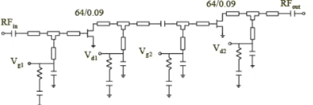
Fig. 1 shows the circuit topology and Fig. 2 shows the chip photo of the power Amplifier. In order to get higher gain in high frequency, we use 8f504 in the last stage, and we use 2f126 in the first stage to driver second stage. In the circuit design, all the transistors are biasing in class A in order to get higher output power and better linearity. We achieve broadband design by using multi-stage transmission line.
From measurement result, this circuit demonstrate small signal gain of better than 18-dB in 41-48GHz, the output power achieve 20dBm.
Sub-Harmonic Diode Mixer
Fig. 3 shows the topology of the mixer, and Fig. 4 shows the chip photo of the sub-harmonic mixer. The core of the mixer is the anti-parallel diode. When the local oscillator signal pumped into diode, due to the nonlinearity of the diode, it will generate higher order harmonics of the local oscillator. The anti-parallel diode will only keep even harmonics of the local oscillator and the mixed mode of the radio frequency remained. By using the characteristic of the diode, we can generate sub-harmonic mixed mode signal.
In the circuit design, we use λ/4 transmission line to do the isolation, and we also use quasi-lumped equivalent circuit to replace long the transmission line in order to decrease the area of the chip. According to the measurement results, this mixer demonstrates conversion loss around 14 dB±2 dB in 38-48 GHz, the isolation between LO to IF around 17 dB.
Linearization of Power Amplifier
The linearity of transmitter mainly is decided by the power amplifier in the front end, so we focus on the linearity of the power amplifier improve the whole transmitter linearity.
Fig. 5 shows the circuit topology of the power amplifier with a low-loss built-in linearizer. We can improve the linearity of the power amplifier by adding a cold mode HEMT in the input. The
benefit of the topology is that we can bias the amplifier through the linearizer without extra biasing circuit. Furthermore, the loss of the linarizer is less than 2 dB, and we can adjust the bias of the linearizer to change the characteristic. In conclusion, it is low loss, small area, no dc power consumption. This linearizer can improve the linearity of the MMW power amplifier.
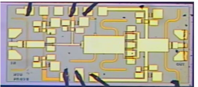
Fig. 6 shows the chip photo of the Power amplifier with linearizer. From measurement result, this circuit demonstrate small signal gain of 8-dB in 44GHz. Fig. 7 shows the comparison between power amplifier with and without linearizer. The linearity of the power amplifier can be effectively improved by adding the linearizer.
Sub-Harmonic Mixer
Fig. 7 shows the topology of the sub-harmonic mixer. The LO power generate 0° and 180° phase difference by a balun, and feed-in the gate of the pHEMT, the RF feed-in the drain of the pHEMT. The drain of the two components are connected to eliminate the odd mode harmonic without effect even mode harmonic. The IF will be extracted by a low pass filter. The LO power needs only 5-dBm, and the chip area is 0.85*0.85 mm2. Such a small chip size makes it easier to be
combined with other circuits. Fig. 8 is the chip photo of the mixer.
From measurement results, as an up-converter, when LO power is 5dBm, LO frequency is 19GHz, the conversion loss around 11-14dB, and P-1dB is -15dBm. As a down-converter, IF frequency is 2-11GHz, it has 13-15dBm conversion loss. The isolation between LO to IF and 2LO to RF are higher than 30dB.
ACPR and IM3R Correlation of Broadband Signal
We try to find out the relationship between ACPRmultitone and IM3R. the relationship between
them is:
We found the relationship can be applied to MMW broadband system, the relationship shows in Fig. 9.
40-48 GHz Ultra Wide Band System Combination
In the system level, we improve the circuit design and applied in system integration. The power amplifier and mixer are replaced by NTU designed devices. We using vector signal generator to generate the 3GHz, 20Mbps, 16-QAM, base-band digital modulation signal, then up-converted to 40-48GHz by mixer, transmitted by transmitter, radiated by antenna. Then we received the signal, and demodulated the received signal by vector signal generator, Fig. 10 is the measured result. It shows that we can correctly demodulate the signal.
Gilbert Cell Mixer
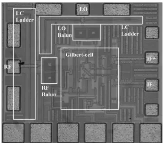
The broadband fully integrated Gilbert-cell mixer is fabricated using TSMC commercial standard 90-nm 1P9M CMOS process. The schematic of the broadband mixer is shown in Fig. 11. The Gilbert-cell configuration is selected for its double-balance implementation which offers high spur suppression in a very compact die size. The LO switching quad consists of two parallel connected NMOS pairs, are biased at near pinch-off region. The performance of the CMOS Gilbert-cell mixer can be improved by using a charge-injection method. With charge-injection circuit switching quad transistors and the voltage drop in load resistors can be reduced. Therefore the value of these load resistors can be increased, thus raising the voltage conversion gain. Two source-follower transistors are added for output impedance matching. The monolithic Marchand- type transformer is used to provide the differential RF and LO signals. In order to improve the bandwidth, the ladder matching networks are introduced in this mixer design. Fig 12 is the chip photo.
From measurement results, with broadband ladder matching networks, the flatness of conversion loss and good RF port return loss over broad bandwidth, from 25 to 75 GHz, can be achieved. The conversion gain is around 3 dB and the RF port return loss is better than 7.5 dB from 25 to 75 GHz. The input 1-dB compression point of the mixer is 2.1 and 4.5 dBm at RF of 40 and 60 GHz, The measured RF to LO and LO to RF isolation are betterthan 30 dB.
Doherty Power Amplifier
The MMW Doherty amplifier is fabricated by 0.15- μm GaAs HEMT MMIC process provided by WIN Semiconductors. Fig. 13 shows the schematic of the Doherty amplifier. It contains a 90o hybrid, a main amplifier, a peaking amplifier,
a quarter-wavelength line, offset lines, and input/output matching networks. The 90o hybrid is
implemented with a Lange coupler which delivers equal input power with 90o phase shift to the main
and peaking amplifier. The common source (CS) connected transistors of the main and peaking amplifiers both employ two-finger 126-μm HEMT device. Both amplifiers are designed to deliver maximum power when presented optimum load impedance. The offset lines are inserted to prevent leakage power from the main amplifier into the peaking amplifier. Therefore, the output power of the main amplifier can be fully delivered to the load. A quarter-wavelength line with correct characteristic impedance is required at the output of the circuit so that the main amplifier and peaking amplifier signals will combine in phase. In MMW Doherty amplifier design, the isolation between main and peaking amplifier must be high enough to avoid coupling effects from degrading the efficiency. Fig. 14 illustrates the chip photo of the MMW Doherty amplifier with a compact chip size of 2.0x1.0 mm2.
On the other hand, the linearity of the Doherty amplifier is determined by main amplifier. To obtain better gain and linearity performance in this MMW Doherty amplifier design, the Class-AB operation is selected for main amplifier. The principle of the post-distortion linearization utilizes a component with gain expansion characteristic to compensate the gain compression and to cancel IMD products at the amplifier output. In IC design stage, the compression characteristic of the Class-AB main amplifier at desirable operation power level can be estimated from simulation. Then the bias point of the Class-C peaking amplifier was adjusted to provide gain expansion at the same operation power level. After recombining the main and peaking amplifiers signals at the output, the linearity performance can be greatly improved.
The measured small signal gain is over 7 dB from 38 to 46 GHz. The input and output return losses are better than 16 dB and 15 dB, respectively. The
saturation output power is 21.8 to 19 dBm from 38 to 46 GHz. The IMD3 of quasi Doherty amplifier can be improved 18 dB at 42 GHz and the drain efficiency improved 6% at 6-dB output back-off compared with the balance amplifier operation.
Balanced Power Amplifier
The use of balanced amplifiers is a practical method for implementing a broadband amplifier that has flat gain, effective power combining, and good input and output return loss. The structure of the Q-band CMOS balanced amplifier is shown in Fig. 15. The CMOS balanced amplifier is constructed with two individual broadband amplifiers and two TFMS broad-side couplers. The input 90° broad-side coupler is known as a 3-dB power divider with 90° phase shift and the output 90° broad-side coupler as a 3-dB power combiner. The isolated port of the 90° broad-side coupler is terminated by on-chip 50Ω resistor. Taking advantage of the multi-level interconnect layers in the 90-nm CMOS process, a TFMS broad-side coupler with a tight coupling factor of 3 dB is implemented using thin-film microstrip line. With the balanced amplifier input and output return loss dependent on the coupler, the individual amplifiers can be designed for broad-bandwidth and flat gain, even if the individual amplifier return loss is high. The schematic of the two-stage individual broadband amplifier is shown in Fig. 16, and Fig. 17. shows the chip photo of the CMOS balanced medium power amplifier with chip size of 0.78×0.92 mm2.
The measured small signal gain is 14.5 dB at 48 GHz with good gain flatness of 13.5 ± 1dB and the 3-dB bandwidth is 37.2 % from 35 to 51 GHz. The balanced medium power amplifier delivers a saturated power of 10.6 dBm and output 1-dB compression points 7.5 dBm. The maximum PAE of 8 % is achieved.
Sub-Harmonic Transmitter with Post- Distortion Linearization
The schematic of the MMW sub-harmonic transmitter is shown in Fig. 18. It consists of a sub-harmonically pumped mixer, a band-pass driver amplifier, and a built-in linearizer. The exceeding LO leakage can saturate the following stage, driver amplifier, and damage the linearity of the transmitter. In conventional transmitter design,
a band-pass filter is required to diminish the LO leakage. However, the bulky band-pass filter increases the chip area. Therefore, to solve the LO leakage problem, the sub-harmonically pumped configuration is selected for the mixer with high fLO-to-fRF and 2fLO-to-fRF isolation in this work. In addition, compared with conventional mixers, the LO frequency of the sub-harmonic mixers is at a one-half frequency of the difference between the RF and IF frequency. Due to the use of an LO at relatively low frequency, the output power and phase noise performance can be superior to the fundamental LO source. To improve the LO leakage problem and eliminate the need for the band-pass filter, the driver amplifier is designed with band-pass frequency response. The driver amplifier is a three stage common source design. In this MMW sub-harmonic transmitter design, due to the finite LO driver power and limited device performance, the small diode size of the anti-parallel pair is selected to get better conversion loss. Therefore, due to the mixer linearity limitation, transmitter reaches its input 1-dB compression point before the driver amplifier input 1-dB compression point which damages the linearity of the transmitter. Therefore a built-in linearizer using a two-finger 150-μm shunt cold mode HEMT transistor is added in third stage of the driver amplifier for post- distortion linearization. The linearizer can provide post-distortion function to compensate the conversion gain compression of the mixer and whole transmitter in the nonlinear region. Fig. 19 is the chip photo.
For the digital signal measurement, the WCDMA signal is up-converted to 40 GHz with a channel power of -2 dBm and a 3.84-MHz channel bandwidth. After linearization, the spectral re-growth suppressed by 8 dB can observed.
四、參考文獻
[1] Katsutoshi tsukamoto, “Development of gigabit millimeter-wave broadband wireless access system - system overview,” Asia-Pacific Microwave Conf. Proc., Dec. 2003.
[2] B. Hughes, J. Orr, G. Martin, “MMIC 20 GHz low-noise and 44 GHz power amplifiers for phased array communication antennas designed for
manufacturability,” IEEE GaAs IC Symp. Dig., pp. 367-370, Oct. 1993.
[3] Y. Jaehyok, Y. Youngoo, P. Myungkyu, K. Wonwoo, K. Bumman, “Analog predistortion linearizer for high-power RF amplifiers,” IEEE Trans. Microwave Theory & Tech., vol. 48, no. 12, pp. 2709-2713, Dec. 2000.
[4] P. Narozny, H. Tobler, G. K. Kornfeld, R. A. Nunn, B. Adelseck, M. Ludwig, G. Eggers, “Pseudomorphic Ku-band GaAs HFET linearizer preamplifier front end for satellite TWT-amplifiers, ” IEEE GaAs IC Symp. Dig., pp. 292-295, Oct. 1995.
[5] K. Yamauchi, M. Nakayama, Y. Ikeda, H. Nakaguro, N. Kadowaki, T. Araki, “An 18 GHz-band MMIC linearizer using a parallel diode with a bias feed resistance and a parallel capacitor,” IEEE MTT-S Int. Microwave Symp. Dig., vol. 3, pp. 1507-1510, June 2000.
[6] A. Katz, S. Moochalla, J. Klatskin, “Passive FET MMIC linearizers for C, X, and Ku-band satellite applications,” IEEE MTT-S Int. Microwave Symp. Dig., vol. 1, pp. 353-356, June 1993.
[7] WIN, Inc., 0.15µm InGaAs pHEMT Power Device Model Handbook, 2003.
[8] Sonnet Software Inc., Sonnet User’s Manual, Release 6.0 Liverpoll, NY, Apr. 1999.
[9] Y. Takimoto, “Research activities on millimeter wave indoor communication systems in Japan, ” IEEE MTT-S Int. Microwave Symp. Digest, pp. 673-676, June 1993. [10] K. Kawakami, M. Shimozawa, H. Ikematsu, K. Itoh, Y.
Isota, and O. Ishida, “A millimeter-wave broadband monolithic even harmonic image rejection mixer,” IEEE MTT-S Int. Microwave Sym., pp. 1443-1446, June 1998. [11] M. Yu, Robert H. Walden, A.E. Schmitz, and M. Lui,
“Ka/Q-band doubly balanced MMIC mixers with low LO power,” IEEE Microwave and Guided Wave Letters, vol. 10, no. 10, pp. 424-426, Oct. 2000. [12] H. Morkner, S. Kumar, and M. Vice, “A 18-45 GHz
double-balanced mixer with integrated LO amplifier and unique suspended broadside-coupled balun,” Gallium Arsenide Integrated Circuit (GaAs IC) Symp., Digest , pp.267-270, Nov. 2003
[13] M.W. Chapman, S. Raman, “A 60-GHz uniplanar MMIC 4
×
subharmonic mixer,” IEEE Transactions on Microwave Theory and Techniques, vol. 50, no. 11, pp. 2580 – 2588, Nov. 2002.[14] H. Okazaki, and Y. Yamaguchi, ”wide-band SSB subharmonically pumped mixer MMIC,” IEEE Trans. Microwave Theory & Tech., vol. 45, no. 12, pp. 2375-2379, Dec. 1997.
[15] C.Y. Chang, C.C. Yang, and D.C. Niu, “A multioctave bandwidth rat-race singly balanced mixer,” IEEE
Microwave and Guided Wave Letters, vol. 9, no. 1, pp. 37-39, Jan. 1999.
[16] Jeng-Han Tsai, Hong-Yeh Chang, Pei-Si Wu, Yi-Lin Lee, Tian-Wei Huang, and Huei Wang, " Design and analysis of a 44-GHz MMIC low-loss built-in linearizer for high-linearity medium power amplifiers," IEEE Trans. on Microwave Theory and Tech., vol. 54, no. 6, pp. 2487-2496, June 2006.
[17] Jeng-Han Tsai, Wei-Chien Chen, To-Po Wang, Tian-Wei Huang, and Huei Wang, " A miniature Q-band low noise amplifier using 0.13- μ m CMOS technology," IEEE Microwave and Guided Wave Letters, vol.16, pp. 327-329, June 2006.
[18] Pei-Si Wu, Hong-Yeh Chang, Ming-Da Tsai, Tian-Wei Huang, Huei Wang, “New miniature 15-20 GHz continuous phase/amplitude control MMICs using 0.18-μm CMOS technology” IEEE Trans. Microwave Theory Tech., vol. 54, no. 1, pp. 10-19, Jan. 2006. [19] Hong-Yeh Chang, Pei-Si Wu, Tian-Wei Huang, Huei
Wang, Chung-Long Chang, and John G.J. Chern, " Design and analysis of CMOS broadband compact high-linearity modulators for gigabit microwave/millimeter-wave applications," IEEE Trans. Microwave Theory Tech., vol. 54, no. 1, pp. 20-30, Jan. 2006
[20]Pei-Si Wu, Chi-Hsueh Wang, Tian-Wei Huang, Huei Wang, “Compact and broadband millimeter-wave monolithic transformer balanced mixers” IEEE Trans. Microwave Theory Tech., vol. 53, no. 10, pp. 3106-3114, Oct. 2005
[21]Hong-Yeh Chang, Jeng-Han Tsai, Tian-Wei Huang, Huei Wang, Yongxiang Xia, and Yonghui Shu, " A W-band high-power predistorted direct-conversion digital modulator for transmitter applications," IEEE Microwave and Guided Wave Letters, vol. 15, no. 9, pp. 600-602, Sept. 2005
[22]Hsiao-Wei Chen, Hsin-Chia Lu and Tian-Wei Huang, “ The analysis of relation between Q-factor and phase noise by using substrate-integrated waveguide cavity oscillators,” Asia-Pacific Microwave Conference Proceedings, Dec. 2005.
[23]Hao-Geng Lin, Tian-Wei Huang, Ruey-Beei Wu, and Chien-Min Lin, “Model extractions of coupled bonding-wire structures in electronic packaging,” Asia-Pacific Microwave Conference Proceedings, vol. I, pp. 275-278 Dec. 2005
[24]Wei-Chien Chen, Jeng-Han Tsai, Shih-Yu Chen, and Tian-Wei Huang, “ACPR and IM3R correlation of broadband signals in microwave and millimeter wave frequencies,” IEEE International Workshop on Radio-Frequency Integration Technology Proceedings,
Nov. 2005.
[25]Wei-Chien Chen, Shih-Yu Chen, Jeng-Han Tsai, Tian-Wei Huang, and Huei Wang, “A 38-48-GHz miniature MMIC subharmonic mixer,” European Microwave Conference Proceedings, Oct. 2005.
[26]Pei-Si Wu, Tian-Wei Huang, and Huei Wang , “A millimeter-wave ultra-compact broadband diode mixer using modified marchand balun,” European Microwave Conference Proceedings, Oct. 2005.
[27]Huei-Han Jhuang, Chi-Hsueh Wang, and Tian-Wei Huang, "65GHz LTCC probing interface design and optimization," IEEE Int. Symp. on Antennas and Propagation Digest, P1.5, July 2005
[28]Hong-Yeh Chang, Pei-Si Wu, Tian-Wei Huang, Huei Wang, Yung-Chih Tsai, and Chun-Hung Chen, " An ultra compact and broadband 15-75 GHz BPSK modulator using 0.13-um CMOS process," IEEE MTT-S Int. Microwave Symp. Digest, June 2005.
[29]Jeng-Han Tsai, Hong-Yeh Chang, Pei-Si Wu, Tian-Wei Huang, and Huei Wang, " A 44-GHz high-linearity MMIC medium power amplifier with a low-loss built-in linearizer," IEEE MTT-S Int. Microwave Symp. Digest, TH2C-2, June 2005
[30]Jeng-Han Tsai, Pei-Si Wu, Chin-Shen Lin, Tian-Wei Huang, Senior Member, IEEE, John G. J. Chern, and Wen-Chu Huang, “A 25–75 GHz broadband Gilbert-Cell mixer using 90-nm CMOS technology,” IEEE Microwave and Wireless Components Letters, vol. 17, no. 4, April 2007
[31]Jeng-Han Tsai, and Tian-Wei Huang, ”A 38–46 GHz MMIC doherty power amplifier using post-distortion linearization,” IEEE Microwave and Wireless Components Letters, vol. 17, no. 5, May 2007
[32]Hong-Yeh Chang, Yi-Hsien Cho, Ming-Fong Lei, Chin-Shen Lin, Tian-Wei Huang, Huei Wang, “A 45-GHz quadrature voltage controlled oscillator with a reflection-type IQ modulator in 0.13- μ m CMOS technology,” IEEE MTT-S International Microwave Symp., Digest, pp.739-742, Jun. 2006
1 2 1 2 1 2 3 4 1 2 3 4 1 2 3 4 1 2 3 4 1 2 3 4 1 2 3 4 1 2 3 Vg1 Vg2 Vd1 Vd2 2f126 8f504 RFIN RFOUT 1 2 1 2 1 2 3 4 1 2 3 4 1 2 3 4 1 2 3 4 1 2 3 4 1 2 3 4 1 2 3 Vg1 Vg2 Vd1 Vd2 2f126 8f504 RFIN RFOUT
Fig. 2. Chip photo of Power Amplifier
Fig. 3. Circuit Topology of the Sub-Harmonic Diode Mixer
Fig. 4. Chip Photo of the Sub-Harmonic Diode Mixer Vg1 Vd1 Vgc Vd2 HEMT1 HEMT2 Vtest
Fig. 5. Circuit topology of the power amplifier with a low loss low-loss built-in linearizer.
linearizer 1.0 mm 1. 0 m m amplifier linearizer 1.0 mm 1. 0 m m amplifier
Fig. 6. Chip Photo of the power amplifier with a low loss low-loss built-in linearizer.
Fig. 7. Circuit topology of the sub-harmonic mixer.
Fig. 8. Chip Photo of the sub-harmonic mixer.
Fig. 9. The comparison between ACPR, Multi-tone ACPR and IM3
Fig. 10. The measure result of 30Msps 16-QAM
Fig. 11. Schematic of fully integrated Gilbert Cell Mixer
Fig. 12. Chip photo of fully integrated Gilbert Cell Mixer
Fig. 13. Schematic of the MMW Doherty PA with post-distortion linearization. -28 -24 -20 -16 -12 -8 -50 -45 -40 -35 -30 -25 -20 -15 -10 -5 0 5 10 18.0 19.5 21.0 22.5 24.0 25.5 27.0 28.5 30.0 31.5 33.0 34.5 36.0 Ga in ( dB ) ACPR ( d Bc ) Input Power (dBm) Measured (64-tone @ 3.84MHz) Calculated (IM3R - 1.17652) Modulated (WCDMA) Gain
Fig. 14. Chip photo of the MMW Doherty PA with post-distortion linearization.
Fig. 15. The structure of the Q-band CMOS balanced amplifier
Fig. 16. The schematic of the two-stage individual broadband amplifier
Fig. 17. The chip photo of the broadband and miniature Q-band CMOS balanced amplifier with chip size of 0.78 × 0.92 mm2.
Fig. 18. Circuit topology of the MMW sub- harmonic transmitter with built-in post-distortion linearizer.
Fig 19. Chip photo of the MMW sub- harmonic transmitter with built-in post-distortion linearizer.
出席國際學術會議心得報告
會議名稱: Asia-Pacific Microwave Conference 亞太 微波會議
會議地點: 日本 橫濱 會議時間: 2006 Dec 11-14 心得報告:
This conference is a good chance to see Japan's advanced wireless technology. During the opening session, NTT report its next generation 4G base-station test. They use four antennas on base station and four antennas on the car roof with speed of 30km/hr. Their MIMO system can achieve 1Gbps high-speed data rate. This speed can be improved to 2.5Gbps with six antenna on both side. This is a ground breaking result for cellular applications, that upgrade the 4G speed from 100Mbps to 1Gbps. This news also encourage our research on MMW gigabit wireless communications.
My student present a paper of monolithic subharmonically pumped resistivemixer, consisting of two pHEMT transistors, a LO reduced-size Marchand balun and RF/IF filters. For years, millimeter-wave
equipments and circuits have been studied and utilized for satellite communication systems and high-speed data communication systems. In these systems, mixers play a key role in these communication systems, especially for
subharmonically pumped mixers. Subharmonic mixers offer an alternative to fundamental mixers in that LO frequency is at half of the fundamental LO frequency. Due to the use of a LO at relatively low frequency, the output power and phase noise performance may be superior to the fundamental LO source. Despite low LO frequency is needed in millimeter-wave system, low LO input power is much desired as well.
The compact RF/IF diplex circuit and a reduced-size balun were used to minimize the chip size which results only 0.72 mm2
. Besides, 5 dBm LO input power is needed which is one-third of other subharmonically pumped mixers with more than 10 dBm LO power. This mixer exhibits 12.5 ± 1.5 dB
up-conversion loss and 12 ± 1 dB
down-conversion loss with 5 dBm LO input power. Up-conversion 1- dB compression output power is -15dBm and downconversion 1-dB compression output power is -12 dBm. To our knowledge, this mixer has good conversion with smallest chip size and
minimum LO input power.
After presentation, our paper has many feedbacks from the audience. One special feature of our mixer is the low LO power, +5dBm, which is lower than +10dBm in traditional sub-harmonic mixer. Our special design of diode bias point selection is appreciated by other MMIC designer.
Proceedings of Asia-Pacific Microwave Conference 2006
A Q-band Miniature Monolithic Subharmonically Pumped
Resistive Mixer
Shih-Yu Chen, Jeng-Han Tsai, Pei-Si Wu, Tian-Wei Huang, and Huei Wang
Department of Electrical Engineering and Graduate Institute of Communication
Engineering, National Taiwan University, Taipei, Taiwan 106, R.O.C.
Tel : +886-02-2363-5251, Fax: +886-02-3366-5084, Email: [email protected]
Abstract — This paper proposes a miniature
Q-band monolithic subharmonically pumped resistive mixer, consisting of two pHEMT transistors, a LO reduced-size Marchand balun and RF/IF filters. The compact RF/IF diplex circuit and a reduced-size balun were used to minimize the chip size which
results only 0.72 mm2. Besides, 5 dBm LO input
power is needed which is one-third of other subharmonically pumped mixers with more than 10
dBm LO power. This mixer exhibits 12.5
±
1.5 dBup-conversion loss and 12
±
1 dB down-conversionloss with 5 dBm LO input power. Up-conversion 1-dB compression output power is -151-dBm and down-conversion 1-dB compression output power is -12 dBm. To our knowledge, this mixer has good conversion with smallest chip size and minimum LO input power.
Index Terms — Marchand balun, MMIC,
millimeter-wave, resistive mixer, subharmonic.
I. INTRODUCTION
For years, millimeter-wave equipments and circuits have been studied and utilized for satellite communication systems and high-speed data communication systems [1]. In these systems, reduction of cost and power consumption is much desired. Mixers play a key role in these communication systems, especially for subharmonically pumped mixers. Subharmonic mixers offer an alternative to fundamental mixers in that LO frequency is at half of the fundamental LO frequency. Due to the use of a LO at relatively low frequency, the output power and phase noise performance may be superior to the fundamental LO source. Despite low LO frequency is needed in millimeter-wave system, low LO input power is much desired as well.
Passive mixers have the advantage of zero DC power consumption, which include diode mixers and resistive mixers. Anti-parallel and ring-quad topologies [2]-[4] have been used most commonly for diode mixers, but they suffer from high LO input power and low linearity. The resistive mixers [5], [6] has been demonstrated to exhibit high linearity, good intermodulation
characteristics, and a natural separation between LO and radio frequency/intermediate frequency (RF/IF) ports. However, the needs of the baluns, band-pass filter and quarter-wave length stub make the chip area of these resistive mixers large.
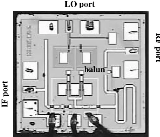
In this paper, we present a Q-band MMIC subharmonically pumped resistive mixer with a compact chip size and low LO input power using 0.15-μm GaAs HEMT MMIC process. To minimize the chip size, a transformer balun consisting of two intertwining spiral coils and compact RF/IF diplexing circuit were used [8]. The presented MMIC achieves the up-conversion loss of 12.5 ± 1.5 dB from 39 to 48 GHz with a miniature chip of 0.72 mm2. Compared with other reported subharmonically pumped resistive mixer [2]-[6], the mixer has good conversion with smallest chip size and requires no off-chip baluns.
II. DEVICE CHARACTERISTIC AND MMICPROCESS
This circuit was fabricated with 0.15-μm GaAs HEMT MMIC process on 100-μm GaAs substrate provided by WIN Semiconductors. The unit current gain frequency (fT) of the device is about 85 GHz, and the maximum oscillation frequency (fmax) is over 200 GHz. Typical breakdown voltage is 10V and the peak of transconductance (Gm) is 495 mS/mm. Other passive components such as thin-film resistors, MIM capacitors, spiral inductors, and air-bridges are available. The 6” wafer is thinned down to 4-mil for the gold plating of the backside, and slot via holes are used for dc grounding [7].
III. CIRCUIT DESIGN
The schematic of the 39-48 GHz subharmonically pumped resistive mixer is shown in Fig. 1. The resistive mixer is composed of a reduced-size Marchand balun, RF/IF diplex circuits and two identical pHEMT transistors with total gate width 100μm in a common source
configuration. Through the balun, the LO signal is pumped to the gates of the devices individually with 180° phase shift, while the RF signal is pumped at the drain in phase through high-pass filter. At low drain voltages, the channel of device operates as a linear resistancecausing frequency mixing.Furthermore, two devices are connected at drains directly to cancel fundamental (odd) harmonic mixing terms without diminishing second-order (even) harmonic mixing terms. The IF signal we need is extracted from the drain through the low pass filter providing RF filtering. Vice versa, if IF signal is pumped into the devices through IF path, the up-converted RF signal will be extracted from the drain and be obtained via RF port.
To minimize chip size, a reduced-size Marchand balun, which composes of two intertwining spiral coils, was used with compact area of 170 x 315 mm2 [8]. Besides, capacitors and quarter-wave lengths were chosen as good RF/IF diplex circuits instead of bulk bandpass filters. Two small capacitors were put in series in the path of RF signal to avoid IF signal from leaking into RF port. Two quarter-wave length lines were designed to block RF signal as band-reject filter preventing RF frequency from leaking to IF port. Fig. 2 shows the fabricated chip photo and the total size is only 0.72 mm2.
Balun
LO
RF IF
Fig. 1. Schematic of the subharmonically pumped resistive mixer.
Fig. 2. Photograph of the resistive mixer chip.
0 2 4 6 8 10 12 14 -30 -25 -20 -15 -10 -5 0 Co nv e rs ion Lo ss (d B) IF freq.(GHz) CL LO input power = 5 dBm LO input frequency = 19GHz IF input power = -30 dBm
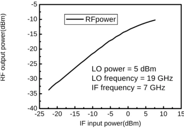
Fig. 3. Up-conversion loss of the subharmonically pumped mixer. -25 -20 -15 -10 -5 0 5 10 15 -40 -35 -30 -25 -20 -15 -10 -5 RF ou tpu t po w e r(dB m ) IF input power(dBm) RFpower LO power = 5 dBm LO frequency = 19 GHz IF frequency = 7 GHz
Fig. 4. IF-RF power of the subharmonically pumped mixer.
IV.MEASUREMENT RESULTS
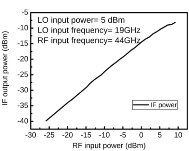
The fabricated chip was measured via probes and the measured up-conversion and down-conversion characteristics are plotted in Fig.3 through Fig.6. Conversion loss is measured at a fixed 19 GHz LO frequency under a 5 dBm LO drive for both up- and down-conversion. In Fig. 3, the mixer exhibits an up-conversion loss of 12.5 ± 1.5 dB having output RF frequency ranges from 39 GHz to 48GHz. As for linearity, the observed 1-dB compression RF output power is -15 dBm under 5 dBm LO power, as shown in Fig. 4 Besides, the measured LO-to-RF isolation is more than 29 dB, and 2LO-to-RF isolation is better than 35 dB.
balun LO port
IF port
On the other hand, Fig.5 depicts the measured down-conversion loss of 12 ± 1dB generating IF frequency from 2 to 11 GHz. The observed 1-dB compression IF output power is -12 dBm under 5 dBm LO power in Fig. 6. The measured LO-to-IF and 2LO-to-RF isolation exceed 30 dB. To sum up, we list all the measured results of this resistive mixer and other reported subharmonically pumped mixers in Table I. It can be easily seen from Table I, the mixer we present has good conversion with smallest chip size and low LO input power.
38 40 42 44 46 48 50 -30 -25 -20 -15 -10 -5 0 Co nv ersi on Los s (dB ) RF freq(GHz) CL LO input power = 5 dBm LO input frequency = 19GHz RF input power = -30 dBm
Fig. 5. Down-conversion loss of the subharmonically pumped mixer. -30 -25 -20 -15 -10 -5 0 5 10 -40 -35 -30 -25 -20 -15 -10 -5 IF ou tp ut p o we r (d B m ) RF input power (dBm) IF power LO input power= 5 dBm LO input frequency= 19GHz RF input frequency= 44GHz
Fig. 6. RF-IF power of the subharmonically pumped mixer.
V.CONCLUSION
A miniature Q-band subharmonically pumped resistive mixer is presented. The compact RF/IF diplexing circuit and a reduced-size balun were used to reduce the chip size which is only 0.72 mm2 while low LO input power is needed. This
mixer exhibit 11-14-dB up-conversion loss and 13-15-dB down-conversion loss with 5 dBm LO power. Good linearity of the mixer is also presented. Up-conversion 1-dB compression output power is -15dBm and down-conversion 1-dB compression output power is -12 1-dBm. To our knowledge, this mixer has good conversion with smallest chip size and minimum LO input power.
ACKNOWLEDGEMENT
This work is supported in part by National Science Council (NSC 95 – 2219 - E - 002 - 011 and NSC 93 - 2752 - E - 002 – 003 -PAE). The chip is fabricated by WIN Semiconductors Corp. through the Chip Implementation Center (CIC), Taiwan, R.O.C.. The authors would like to thank Yi-Lin Lee and Sheng-Yan Chen of National Taiwan Univ. for the help of measurement setup.
REFERENCES
[1] Katsutoshi Tsukamoto, et.al., “Development of gigabit Millimeter-Wave broadband wireless access system - system overview,” in Proc. Asia-Pacific Microwave Conf., Seoul, Korea, 2003, pp. 957-960.
[2] H. Morkner, S. Kumar, and M. Vice, “A 18-45 GHz double-balanced mixer with integrated LO amplifier and unique suspended broadside-coupled balun,” 2003 Gallium Arsenide Integrated Circuit Symposium, pp. 267-270, November 2003. [3] K. Kawakami, M. Shimozawa, H. Ikematsu, K.
Itoh, Y. Isota, and O. Ishida, “A millimeter-wave broadband monolithic even harmonic image rejection mixer,”1998 IEEE MTT-S Int. Microwave Sym., pp. 1443-1446, June 1998.
[4] W.-C. Chen, S.-Y. Chen, J.-H. Tsai, T.-W. Huang, and H. Wang, “A 38-48-GHz miniature MMIC subharmonic mixer,” in European Microwave Conference Proceedings, Oct. 2005.
[5] K. S. Ang, A. H. Baree, S. Nam, and I. D. Robertson, “A millimeter-wave monolithic sub-harmonically pumped resistive mixer,” in Proc. Asia-Pacific Microwave Conf., vol. 2, pp. 222-225, 1999.
[6] M.-F. Lei, P.-S. Wu, T.-W. Huang, H. Wang, ” Design and analysis of a miniature W-band MMIC subharmonically pumped resistive mixer,” 2004 IEEE MTT-S Int. Microwave Sym., vol. 1, pp. 235-238, June 2004.
[7] WIN, Inc., 0.15 μm InGaAs pHEMT Power DeviceModel Handbook, 2003.
[8] P.-S. Wu, C.-H. Tseng, T.-W. Huang, and H. Wang, “A singly balanced millimeter-wave mixer using a compact transformer,” 2003 APMC Digest, vol. 3, pp. 649-652, Nov. 2003.
TABLEI
PERFORMANCE COMPARISON OF REPORTED SUBHARMONICALLY PUMED MIXER
Reference Technology RF(GHz) CL(dB) LO (dBm) Chip size(mm2) Mixing type
[2] GaAs
pHEMT 18-45 10-12 17 0.73
Ring- quad diode mixer [3] GaAs HEMT 24-44 13-16 16 3.48 Anti-parallel diode mixer [4] GaAs pHEMT 38-48 12-15 10 0.72 Anti-parallel diode mixer [5] GaAs pHEMT 34-40 9.5-13 5 2.31 Resistive mixer [6] GaAs pHEMT 75-88 14-18 5 1.50 Resistive mixer
This work GaAs
pHEMT 39-48 11-14 5 0.72
出席國際學術會議心得報告
會議名稱: Asia-Pacific Microwave Conference 亞太 微波會議
會議地點: 日本 橫濱 會議時間: 2006 Dec 11-14 心得報告:
This conference is a good chance to see Japan's advanced wireless technology. During the opening session, NTT report its next generation 4G base-station test. They use four antennas on base station and four antennas on the car roof with speed of 30km/hr. Their MIMO system can achieve 1Gbps high-speed data rate. This speed can be improved to 2.5Gbps with six antenna on both side. This is a ground breaking result for cellular applications, that upgrade the 4G speed from 100Mbps to 1Gbps. This news also encourage our research on MMW gigabit wireless communications.
My student present a paper of monolithic subharmonically pumped resistivemixer, consisting of two pHEMT transistors, a LO reduced-size Marchand balun and RF/IF filters. For years, millimeter-wave
equipments and circuits have been studied and utilized for satellite communication systems and high-speed data communication systems. In these systems, mixers play a key role in these communication systems, especially for
subharmonically pumped mixers. Subharmonic mixers offer an alternative to fundamental mixers in that LO frequency is at half of the fundamental LO frequency. Due to the use of a LO at relatively low frequency, the output power and phase noise performance may be superior to the fundamental LO source. Despite low LO frequency is needed in millimeter-wave system, low LO input power is much desired as well.
The compact RF/IF diplex circuit and a reduced-size balun were used to minimize the chip size which results only 0.72 mm2
. Besides, 5 dBm LO input power is needed which is one-third of other subharmonically pumped mixers with more than 10 dBm LO power. This mixer exhibits 12.5 ± 1.5 dB
up-conversion loss and 12 ± 1 dB
down-conversion loss with 5 dBm LO input power. Up-conversion 1- dB compression output power is -15dBm and downconversion 1-dB compression output power is -12 dBm. To our knowledge, this mixer has good conversion with smallest chip size and
minimum LO input power.
After presentation, our paper has many feedbacks from the audience. One special feature of our mixer is the low LO power, +5dBm, which is lower than +10dBm in traditional sub-harmonic mixer. Our special design of diode bias point selection is appreciated by other MMIC designer.
Proceedings of Asia-Pacific Microwave Conference 2006
A Q-band Miniature Monolithic Subharmonically Pumped
Resistive Mixer
Shih-Yu Chen, Jeng-Han Tsai, Pei-Si Wu, Tian-Wei Huang, and Huei Wang
Department of Electrical Engineering and Graduate Institute of Communication
Engineering, National Taiwan University, Taipei, Taiwan 106, R.O.C.
Tel : +886-02-2363-5251, Fax: +886-02-3366-5084, Email: [email protected]
Abstract — This paper proposes a miniature
Q-band monolithic subharmonically pumped resistive mixer, consisting of two pHEMT transistors, a LO reduced-size Marchand balun and RF/IF filters. The compact RF/IF diplex circuit and a reduced-size balun were used to minimize the chip size which
results only 0.72 mm2. Besides, 5 dBm LO input
power is needed which is one-third of other subharmonically pumped mixers with more than 10
dBm LO power. This mixer exhibits 12.5
±
1.5 dBup-conversion loss and 12
±
1 dB down-conversionloss with 5 dBm LO input power. Up-conversion 1-dB compression output power is -151-dBm and down-conversion 1-dB compression output power is -12 dBm. To our knowledge, this mixer has good conversion with smallest chip size and minimum LO input power.
Index Terms — Marchand balun, MMIC,
millimeter-wave, resistive mixer, subharmonic.
I. INTRODUCTION
For years, millimeter-wave equipments and circuits have been studied and utilized for satellite communication systems and high-speed data communication systems [1]. In these systems, reduction of cost and power consumption is much desired. Mixers play a key role in these communication systems, especially for subharmonically pumped mixers. Subharmonic mixers offer an alternative to fundamental mixers in that LO frequency is at half of the fundamental LO frequency. Due to the use of a LO at relatively low frequency, the output power and phase noise performance may be superior to the fundamental LO source. Despite low LO frequency is needed in millimeter-wave system, low LO input power is much desired as well.
Passive mixers have the advantage of zero DC power consumption, which include diode mixers and resistive mixers. Anti-parallel and ring-quad topologies [2]-[4] have been used most commonly for diode mixers, but they suffer from high LO input power and low linearity. The resistive mixers [5], [6] has been demonstrated to exhibit high linearity, good intermodulation
characteristics, and a natural separation between LO and radio frequency/intermediate frequency (RF/IF) ports. However, the needs of the baluns, band-pass filter and quarter-wave length stub make the chip area of these resistive mixers large.
In this paper, we present a Q-band MMIC subharmonically pumped resistive mixer with a compact chip size and low LO input power using 0.15-μm GaAs HEMT MMIC process. To minimize the chip size, a transformer balun consisting of two intertwining spiral coils and compact RF/IF diplexing circuit were used [8]. The presented MMIC achieves the up-conversion loss of 12.5 ± 1.5 dB from 39 to 48 GHz with a miniature chip of 0.72 mm2. Compared with other reported subharmonically pumped resistive mixer [2]-[6], the mixer has good conversion with smallest chip size and requires no off-chip baluns.
II. DEVICE CHARACTERISTIC AND MMICPROCESS
This circuit was fabricated with 0.15-μm GaAs HEMT MMIC process on 100-μm GaAs substrate provided by WIN Semiconductors. The unit current gain frequency (fT) of the device is about 85 GHz, and the maximum oscillation frequency (fmax) is over 200 GHz. Typical breakdown voltage is 10V and the peak of transconductance (Gm) is 495 mS/mm. Other passive components such as thin-film resistors, MIM capacitors, spiral inductors, and air-bridges are available. The 6” wafer is thinned down to 4-mil for the gold plating of the backside, and slot via holes are used for dc grounding [7].
III. CIRCUIT DESIGN
The schematic of the 39-48 GHz subharmonically pumped resistive mixer is shown in Fig. 1. The resistive mixer is composed of a reduced-size Marchand balun, RF/IF diplex circuits and two identical pHEMT transistors with total gate width 100μm in a common source
configuration. Through the balun, the LO signal is pumped to the gates of the devices individually with 180° phase shift, while the RF signal is pumped at the drain in phase through high-pass filter. At low drain voltages, the channel of device operates as a linear resistancecausing frequency mixing.Furthermore, two devices are connected at drains directly to cancel fundamental (odd) harmonic mixing terms without diminishing second-order (even) harmonic mixing terms. The IF signal we need is extracted from the drain through the low pass filter providing RF filtering. Vice versa, if IF signal is pumped into the devices through IF path, the up-converted RF signal will be extracted from the drain and be obtained via RF port.
To minimize chip size, a reduced-size Marchand balun, which composes of two intertwining spiral coils, was used with compact area of 170 x 315 mm2 [8]. Besides, capacitors and quarter-wave lengths were chosen as good RF/IF diplex circuits instead of bulk bandpass filters. Two small capacitors were put in series in the path of RF signal to avoid IF signal from leaking into RF port. Two quarter-wave length lines were designed to block RF signal as band-reject filter preventing RF frequency from leaking to IF port. Fig. 2 shows the fabricated chip photo and the total size is only 0.72 mm2.
Balun
LO
RF IF
Fig. 1. Schematic of the subharmonically pumped resistive mixer.
Fig. 2. Photograph of the resistive mixer chip.
0 2 4 6 8 10 12 14 -30 -25 -20 -15 -10 -5 0 Co nv e rs ion Lo ss (d B) IF freq.(GHz) CL LO input power = 5 dBm LO input frequency = 19GHz IF input power = -30 dBm
Fig. 3. Up-conversion loss of the subharmonically pumped mixer. -25 -20 -15 -10 -5 0 5 10 15 -40 -35 -30 -25 -20 -15 -10 -5 RF ou tpu t po w e r(dB m ) IF input power(dBm) RFpower LO power = 5 dBm LO frequency = 19 GHz IF frequency = 7 GHz
Fig. 4. IF-RF power of the subharmonically pumped mixer.
IV.MEASUREMENT RESULTS
The fabricated chip was measured via probes and the measured up-conversion and down-conversion characteristics are plotted in Fig.3 through Fig.6. Conversion loss is measured at a fixed 19 GHz LO frequency under a 5 dBm LO drive for both up- and down-conversion. In Fig. 3, the mixer exhibits an up-conversion loss of 12.5 ± 1.5 dB having output RF frequency ranges from 39 GHz to 48GHz. As for linearity, the observed 1-dB compression RF output power is -15 dBm under 5 dBm LO power, as shown in Fig. 4 Besides, the measured LO-to-RF isolation is more than 29 dB, and 2LO-to-RF isolation is better than 35 dB.
balun LO port
IF port
On the other hand, Fig.5 depicts the measured down-conversion loss of 12 ± 1dB generating IF frequency from 2 to 11 GHz. The observed 1-dB compression IF output power is -12 dBm under 5 dBm LO power in Fig. 6. The measured LO-to-IF and 2LO-to-RF isolation exceed 30 dB. To sum up, we list all the measured results of this resistive mixer and other reported subharmonically pumped mixers in Table I. It can be easily seen from Table I, the mixer we present has good conversion with smallest chip size and low LO input power.
38 40 42 44 46 48 50 -30 -25 -20 -15 -10 -5 0 Co nv ersi on Los s (dB ) RF freq(GHz) CL LO input power = 5 dBm LO input frequency = 19GHz RF input power = -30 dBm
Fig. 5. Down-conversion loss of the subharmonically pumped mixer. -30 -25 -20 -15 -10 -5 0 5 10 -40 -35 -30 -25 -20 -15 -10 -5 IF ou tp ut p o we r (d B m ) RF input power (dBm) IF power LO input power= 5 dBm LO input frequency= 19GHz RF input frequency= 44GHz
Fig. 6. RF-IF power of the subharmonically pumped mixer.
V.CONCLUSION
A miniature Q-band subharmonically pumped resistive mixer is presented. The compact RF/IF diplexing circuit and a reduced-size balun were used to reduce the chip size which is only 0.72 mm2 while low LO input power is needed. This
mixer exhibit 11-14-dB up-conversion loss and 13-15-dB down-conversion loss with 5 dBm LO power. Good linearity of the mixer is also presented. Up-conversion 1-dB compression output power is -15dBm and down-conversion 1-dB compression output power is -12 1-dBm. To our knowledge, this mixer has good conversion with smallest chip size and minimum LO input power.
ACKNOWLEDGEMENT
This work is supported in part by National Science Council (NSC 95 – 2219 - E - 002 - 011 and NSC 93 - 2752 - E - 002 – 003 -PAE). The chip is fabricated by WIN Semiconductors Corp. through the Chip Implementation Center (CIC), Taiwan, R.O.C.. The authors would like to thank Yi-Lin Lee and Sheng-Yan Chen of National Taiwan Univ. for the help of measurement setup.
REFERENCES
[1] Katsutoshi Tsukamoto, et.al., “Development of gigabit Millimeter-Wave broadband wireless access system - system overview,” in Proc. Asia-Pacific Microwave Conf., Seoul, Korea, 2003, pp. 957-960.
[2] H. Morkner, S. Kumar, and M. Vice, “A 18-45 GHz double-balanced mixer with integrated LO amplifier and unique suspended broadside-coupled balun,” 2003 Gallium Arsenide Integrated Circuit Symposium, pp. 267-270, November 2003. [3] K. Kawakami, M. Shimozawa, H. Ikematsu, K.
Itoh, Y. Isota, and O. Ishida, “A millimeter-wave broadband monolithic even harmonic image rejection mixer,”1998 IEEE MTT-S Int. Microwave Sym., pp. 1443-1446, June 1998.
[4] W.-C. Chen, S.-Y. Chen, J.-H. Tsai, T.-W. Huang, and H. Wang, “A 38-48-GHz miniature MMIC subharmonic mixer,” in European Microwave Conference Proceedings, Oct. 2005.
[5] K. S. Ang, A. H. Baree, S. Nam, and I. D. Robertson, “A millimeter-wave monolithic sub-harmonically pumped resistive mixer,” in Proc. Asia-Pacific Microwave Conf., vol. 2, pp. 222-225, 1999.
[6] M.-F. Lei, P.-S. Wu, T.-W. Huang, H. Wang, ” Design and analysis of a miniature W-band MMIC subharmonically pumped resistive mixer,” 2004 IEEE MTT-S Int. Microwave Sym., vol. 1, pp. 235-238, June 2004.
[7] WIN, Inc., 0.15 μm InGaAs pHEMT Power DeviceModel Handbook, 2003.
[8] P.-S. Wu, C.-H. Tseng, T.-W. Huang, and H. Wang, “A singly balanced millimeter-wave mixer using a compact transformer,” 2003 APMC Digest, vol. 3, pp. 649-652, Nov. 2003.
TABLEI
PERFORMANCE COMPARISON OF REPORTED SUBHARMONICALLY PUMED MIXER
Reference Technology RF(GHz) CL(dB) LO (dBm) Chip size(mm2) Mixing type
[2] GaAs
pHEMT 18-45 10-12 17 0.73
Ring- quad diode mixer [3] GaAs HEMT 24-44 13-16 16 3.48 Anti-parallel diode mixer [4] GaAs pHEMT 38-48 12-15 10 0.72 Anti-parallel diode mixer [5] GaAs pHEMT 34-40 9.5-13 5 2.31 Resistive mixer [6] GaAs pHEMT 75-88 14-18 5 1.50 Resistive mixer
This work GaAs
pHEMT 39-48 11-14 5 0.72