非同步8051微控器之解碼器設計
44
0
0
全文
(2) 非同步 8051 微控器之解碼器設計 Decoder Design of the Asynchronous 8051 Microcontroller 研 究 生:王端傑. Student:Tuan-Chieh Wang. 指導教授:陳昌居. Advisor:Chang-Jiu Chen. 國 立 交 通 大 學 資 訊 科 學 與 工 程 研 究 所 碩 士 論 文. A Thesis Submitted to Institute of Computer Science and Engineering College of Computer Science National Chiao Tung University in partial Fulfillment of the Requirements for the Degree of Master in Computer Science June 2006 Hsinchu, Taiwan, Republic of China. 中華民國九十五年六月.
(3) 非同步 8051 微控器之解碼器設計. 研究生:王端傑. 指導教授:陳昌居 國立交通大學 資訊科學與工程學系 摘要. 近來可攜式裝置的使用越來越普遍,因此低耗電的設計成為重要的目標,由 於資料驅動的特性使得非同步電路適用於低耗電設計,我們會提出一個新的非同 步 8051 微控制器的解碼器設計,這是由於 8051 是最普遍使用的解碼器之一,而 且往往在其應用上低耗電特性是相當重要的。 在 本 論 文 中 電 路 設 計 使 用 Balsa 語 言 , 一 種 以 CSP (Communication Sequential Process)為基礎的非同步電路硬體描述語言並且可以合成非同步電 路,由 Balsa 可以合成適用於 Xilinx 合成器的 Verilog netlist,我們可以比 較非同步與同步電路在 Xilinx FPGA 上的表現或使用其它 CAD 工具來實現晶片設 計.. i.
(4) Decoder Design of the Asynchronous 8051 Microcontroller. Student :Tuan-Chieh Wang Advisor : Dr. Chang-Jiu Chen Department of Computer Science National Chiao-Tung University. Abstract Recently mobile devices have been popularly used, and low power is becoming an import subject. With the data-driven feature, the asynchronous circuit is suited to be used for low-power design. We will propose a new decoder design of the asynchronous 8051 microcontroller because the 8051 is one of the most popular microcontroller and is often used in applications where low energy consumption is important. The circuit is a complied VLSI-program, using Balsa as VLSI-programming language which is a CSP-based asynchronous hardware description language and synthesis tool. A Verilog netlist for XST (XILINX Synthesis Tool) is generated by Balsa. We will compare asynchronous 8051 and synchronous 8051 in XILINX FPGA and then use Cadence tools and Synopsys tools to synthesis the layout of the circuit.. ii.
(5) Acknowledgment 完成這篇論文要感謝眾多在我週遭幫助我的人,首先是陳昌居老師在這兩年 的辛苦指導,另外是鄭緯民學長熱心的協助我論文的完成,還有蔡瑞夫同學的合 作,另外實驗室的其他同學與學弟也給我很多的支持與鼓勵,最後還要感謝我的 家人,讓我能夠安穩的完成學業。. iii.
(6) CONTENTS 摘要 ................................................................................................................................i ABSTRACT..................................................................................................................ii ACKNOWLEDGMENT ........................................................................................... iii CONTENTS ................................................................................................................iv LIST OF FIGURES ....................................................................................................vi LIST OF TABLES......................................................................................................vii CHAPTER 1 INTRODUCTION................................................................................1 1-1 Motivations.....................................................................................................1 1-2 Asynchronous circuit design .........................................................................1 1-3 Balsa synthesis tool ........................................................................................3 1-4 The organization of this thesis......................................................................5 CHAPTER 2 RELATED WORKS.............................................................................6 2-1 Overview of 8051 ...........................................................................................6 2-2 Instruction Set................................................................................................7 2-3 Balsa Back-End............................................................................................ 11 2-3-1 Basic Elements.................................................................................. 11 2-3-2 Handshake Components..................................................................14 CHAPTER 3 THE DESIGN .....................................................................................18 3-1 The architecture of the pipelined asynchronous 8051..............................18 3-2 The design of IF stage..................................................................................19 3-2-1 Mem Interface ..................................................................................19 3-2-2 Buffers ...............................................................................................20 3-2-2 Fetcher Ctrl.......................................................................................21 3-3 The design of ID stage .................................................................................22. iv.
(7) 3-3-1 The ID1 stage ....................................................................................22 3-3-2 The ID2 stage ....................................................................................23 CHAPTER 4 IMPLEMENTATION AND VERIFICATION ................................25 4-1 The design flow of FPGA ............................................................................25 4-2 Verification ...................................................................................................26 CHAPTER 5 THE RESULT.....................................................................................29 5-1 Simulation result..........................................................................................29 5-1-1 The performance of the decoder .....................................................29 5-1-2 The performance of the pipelined asynchronous 8051 .................30 5-2 Area cost .......................................................................................................31 5-3 The discussion of the result.........................................................................32 CHAPTER 6 CONCLUSIONS AND FUTURE WORKS .....................................34 REFERENCE.............................................................................................................35. v.
(8) LIST OF FIGURES 1-1 An example of asynchronous circuit ....................................................................2 1-2 Balsa design flow....................................................................................................4 2-1 Architecture of 8051 core ......................................................................................7 2-2 Eight addressing mode ..........................................................................................9 2-3 The Muller C-element .........................................................................................12 2-4 The NC2P-element...............................................................................................13 2-5 The S-element.......................................................................................................13 2-6 The multiplexer....................................................................................................14 2-7 The de-multiplexer ..............................................................................................14 2-8 The Fetch Component .........................................................................................15 2-9 The Sequence Component ..................................................................................15 2-10 The Concurrent Component.............................................................................16 2-11 The Variable Component ..................................................................................16 3-1 The architecture of asynchronous pipelined 8051 ............................................18 3-2 The architecture of IF stage ................................................................................19 3-3 the flow chart of the mem interface ...................................................................20 3-4 the flow chart of the buffer .................................................................................21 3-5 the flow chart of the fetcher ctrl.........................................................................21 3-6 The architecture of ID stage ...............................................................................22 3-7 The flow chart of the ID1 stage ..........................................................................23 3-8 The flow chart of the ID2 stage ..........................................................................24 4-1 The FPGA design flow.........................................................................................26 4-2 PA8051 simulation environment ........................................................................27 4-3 THE ROM MODEL............................................................................................28 vi.
(9) LIST OF TABLES 2-1 ISA of 8051 ...........................................................................................................10 5-1 The comparison of different numbers of buffers..............................................29 5-2 The comparison of different sizes of buffers .....................................................30 5-3 The The performance of the whole pipelined asynchronous 8051 with different sizes of buffers ............................................................................................30 5-4 The comparison between the 1-cycle asynchronous 8051 and the pipelined asynchronous 8051 .....................................................................................................31 5-5 The Cost of Every Part of 8051 ..........................................................................32. vii.
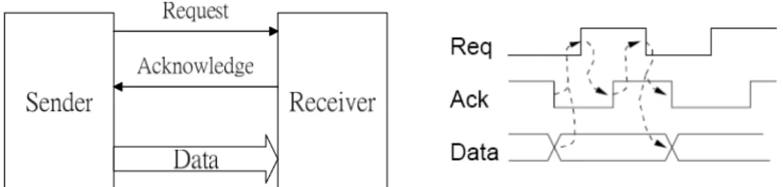
(10) Chapter 1 INTRODUCTION The goal of this thesis is to design and implement a new decoder for a pipelined asynchronous 8051 microcontroller. In this chapter, section 1 describes the motivation of decoder design of asynchronous 8051 microcontroller. Section 2 discusses the advantages and challenges of the asynchronous circuit design. Section 3 describes the Balsa synthesis tool. Session 4 describes the organization of this thesis.. 1-1 Motivations Research in asynchronous circuit design can be traced back to the mid 1950s, however, because of testability and easy to design issues, synchronous design becomes the major technology of digital circuit design. However, in the late 1990s projects in academia and industry demonstrated that it is possible to design asynchronous circuits which exhibit significant benefits in nontrivial real-life examples, and therefore commercialization of the technology began to take place. We hope to design a new decoder with low power and high performance features, and thus the asynchronous design technology is the one we chose for this purpose.. 1-2 Asynchronous circuit design Because the asynchronous circuit works only when necessary, it has the potential for low power consumption. However, it is quite difficult to design the asynchronous circuit because of its complex handshake circuits. An example of asynchronous circuit is shown in figure 1-1. 1.
(11) Figure 1-1 An example of asynchronous circuit This is so the called four-phase bundled data handshake protocol. When the data of the sender is ready, the sender pulls up the request signal, Req, and then the receiver also pulls up the acknowledge signal, Ack, and receives the data at the same time. At the end, both the sender and the receiver pull down the Req and the Ack, and the handshake is completed. By using the handshake protocol, there are several advantages of asynchronous circuit. z. Low power consumption Due to fine-grain clock gating and zero standby power consumption.. z. High operating speed Operating speed is determined by actual local latencies rather than global worst-case latency.. z. Less emission of electro-magnetic noise The local clocks tend to tick at random points in time.. z. Robustness towards variations in supply voltage, temperature, and fabrication process parameters Timing is based on matched delays (and can even be insensitive to circuit and wire delays).. z. Better composability and modularity Because of the simple handshake interfaces and the local timing.. 2.
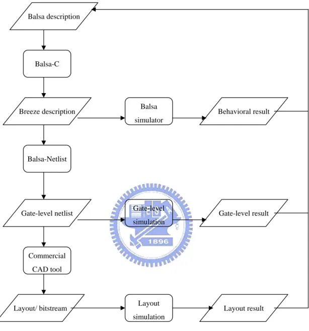
(12) z. No clock distribution and clock skew problems There is no global signal that needs to be distributed with minimal phase skew across the circuit.. On the other hand there are also some drawbacks. z. Overhead (area, speed, power) The additional handshake control circuits.. z. Hard to design Converting sync to async is hard to achieve the results.. z. Few CAD tools There are few CAD tools for asynchronous design.. 1-3 Balsa synthesis tool There is a synthesis tool for asynchronous circuits, Balsa[1], which is developed at Manchester University. This tool uses a language, Balsa, which is a CSP-based language, and is easily used to describe behaviors of asynchronous circuit. The Balsa program would be compiled automatically into a handshake circuit description. The handshake circuits are composed about 40 basic components which use handshake for communication. This tool can also provide behavioral simulations and a transformation from handshake circuits to gate-level netlists. The design flow is shown in the figure 1-2.. 3.
(13) Balsa description. Balsa-C. Breeze description. Balsa. Behavioral result. simulator. Balsa-Netlist. Gate-level netlist. Gate-level. Gate-level result. simulation. Commercial CAD tool. Layout/ bitstream. Layout. Layout result. simulation. Figure 1-2 Balsa design flow The designer writes the Balsa description, and then compiles it with Balsa synthesis tool. It will construct a Breeze description which describes the netlist of handshake components. We can use the Breeze description to do Balsa behavioural simulation or to convert it to Verilog gate level netlist.. 4.
(14) 1-4 The organization of this thesis In this thesis, we will illustrate the related work in chapter 2 including the overview and the instruction set of the 8051, the back-end of the Balsa synthesis system. In chapter 3 we will illustrate the decoder design of asynchronous pipelined 8051. In chapter 4 we will illustrate the implementation and verification. In chapter 5 we will illustrate the results. Finally, a brief conclusion and future work are discussed in chapter 7.. 5.
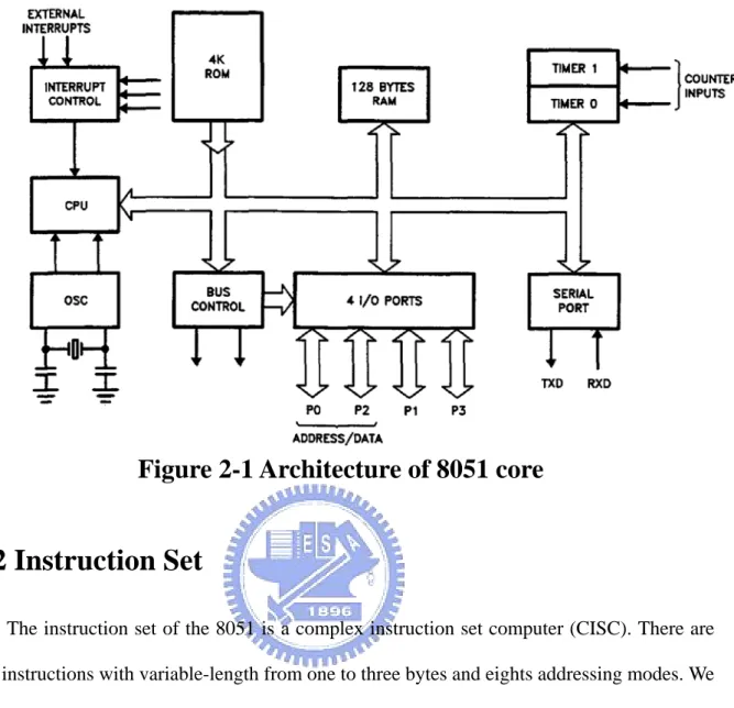
(15) Chapter 2 Related Works In this section we will describe the instruction set and the architecture of the Intel 8051[5]. Then, we will illustrate the back-end of the balsa synthesis system.. 2-1 Overview of 8051 The 8051 is the original member of the MCS-51 family, and is the core for all MCS-51 devices. The features of the 8051 core are z. 8-bit CPU optimized for control applications. z. Extensive Boolean processing (Single-blt logic) capabtilties. z. 64K Program Memory address space. z. 64K Data Memory address space. z. 32 bidirectional and individually addressable 1/0 lines. z. Two 16-bit timer/counters. z. Full duplex UART. z. 6-source/5-vector interrupt structure with two priority levels. z. On-chip clock oscillator. The basic architecture of the 8051 core is shown in figure 2-1.. 6.
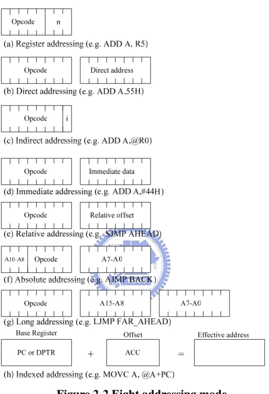
(16) Figure 2-1 Architecture of 8051 core. 2-2 Instruction Set The instruction set of the 8051 is a complex instruction set computer (CISC). There are 255 instructions with variable-length from one to three bytes and eights addressing modes. We can determine an instruction from the first byte of an instruction and the remained bytes always are operands. Besides, the 8051 is a Havard architecture and its instruction memory and data memory are separate. The eight addressing modes are depicted in figure 2-2: (a) register addressing: instructions are encoded using the three least-significant bits of the instruction opcode. (b) direct addressing: the operand is specified by an 8-bit address field in the instruction representing an address in the internal data RAM or a special-function register (SFR). (c) indirect addressing: the instruction specifies a register (R0 or R1) containing the address of the operand in data memory. 7.
(17) (d) immediate addressing: the constant operand value is part of the instruction. (e) relative addressing: a relative address (or offset) is an 8-bit signed value, which is added to the program counter to form the address of the next instruction executed. (f) absolute addressing: these instructions allow branching within the current 2K page of code memory by providing the 11 least-significant bits of the destination address. (g) long addressing: these instructions include a full 16-bit destination address as bytes 2 and 3 of the instruction. (h) indexed addressing: uses a base register (either the program counter or the data pointer) and an offset (the accumulator) in forming the effective address for a JMP or MOVC instruction.. 8.
(18) Figure 2-2 Eight addressing mode. 9.
(19) H. 0. 1. 2. 3. 4. 5. 6. 7. 8. 9. A. B. C. D. E. F. NOP. JBC. JB. JNB. JC. JNC. JZ. JNZ. SJMP. MOV. ORL. ANL. PUSH. POP. MOVX. MOVX. bit,rel. bit,rel. bit,rel. rel. rel. rel. rel. rel. DPTR,#. C,/bit. C,/bit. dir. dir. A,. @DPTR,. @DPTR. A. L 0. dara 16 1. AJMP. ACALL. AJMP. ACALL. AJMP. ACALL. AJMP. ACALL. AJMP. ACALL. AJMP. ACALL. AJMP. ACALL. AJMP. ACALL. 2. LJMP. LCALL. RET. RETI. ORL. ANL. XRL. ORL. ANL. MOV. MOV. CPL. CLR. SETB. MOVX. MOVX. addr16. addr16. dir,A. dir,A. dir,A. C,bit. C,bit. bit,C. C,bit. bit. bit. bit. A,@R0. @R0,A. RR. RRC. RL. RLC. ORL. ANL. XRL. JMP. MOVC. MOVC. INC. CPL. CLR. SET. MOVX. MOVX. A. A. A. A. dir,#data. dir,#data. dir,#data. @A+DPTR. A,@A+PC. A,@A+DPTR. DPTR. C. C. C. A,@R1. @R1,A. INC. DEC. ADD. ADDC. ORL. ANL. XRL. MOV. DIV. SUBB. MUL. CJNE A,. SWAP. DA. CLR. CPL. A. A. A,#data. A,#data. A,#data. A,#data. A,#data. A,#data. AB. A,#data. AB. #data,. A. A. A. A. 3. 4. rel 5. 6-7. INC. DEC. ADD. ADDC. ORL. ANL. XRL. MOV. MOV. SUBB. CJNE A,. XCH. DJNZ. MOV. MOV. dir. dir. A,dir. A,dir. A,dir. A,dir. A,dir. dir,#data. dir,dir. A,dir. dir,rel. A,dir. dir,rel. A,dir. dir,A. INC. DEC. ADD. ADDC. ORL. ANL. XRL. MOV. MOV. SUBB. MOV. CJNE. XCH. XCHD. MOV. MOV. @Ri. @Ri. A,@Ri. A,@Ri. A,@Ri. A,@Ri. A,@Ri. @Ri,#data. dir,@Ri. A,@Ri. @Ri,dir. @Ri. A,@Ri. A,@Ri. A,@Ri. @Ri,A. ,#data ,rel 8-F. INC. DEC. ADD. ADDC. ORL. ANL. XRL. MOV. MOV. SUBB. MOV. CJNE. XCH. DJNZ. MOV. MOV. Rn. Rn. A,Rn. A,Rn. A,Rn. A,Rn. A,Rn. Rn,#data. dir,Rn. A,Rn. Rn,dir. Rn. A,Rn. Rn,rel. A,Rn. Rn,A. ,#data ,rel. Table 2-1 ISA of 8051 10.
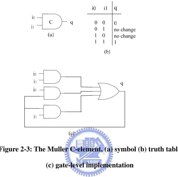
(20) Table 2-1 illustrates the full instruction set of 8051. We can determine an instruction from the first byte. In this table the rows represent the four least significant bits of the opcode while the columns represent the four most significant bits. In addition, Row 8-F are instructions of register addressing, and the register which is used is according to the last three bits. Row 6-7 are instructions of indirect addressing, and the last bit indicates which register (R0 or R1) will be used as indirect address. And A5H is reserved.. 2-3 Balsa Back-End The Balsa synthesis system could convert handshake circuits into gate-level netlists. The netlists are composed by the standard cells of the Xliinx FPGA. We will describe basic some handshake components in Balsa synthesis system.. 2-3-1 Basic Elements The standard cells of Xilinx FPGA used by Balsa are AND, OR, NOR, XOR, NADN, BUF, XNOR, INV, FD (D-type flip-flop), FDC and FDCE. And the most basic cell in asynchronous circuit is the Muller C-element as shown in Figure 2-3. It is a sequential circuit which holds the past state. With all-0 inputs, the output is set to 0. With all-1 inputs, the output is set to 1. With other inputs, the output does not change. A Muller C-element is a fundamental component that is extensively used in asynchronous circuits.. 11.
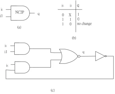
(21) Figure 2-3: The Muller C-element, (a) symbol (b) truth table (c) gate-level implementation. Figure 2-4 shows the NC2P element. It behaves a little like a C-element. When i0 is equal to 0, the output is 0. When i0 and i1 are equal to 1, the output is 1. With other inputs , the output does not change.. 12.
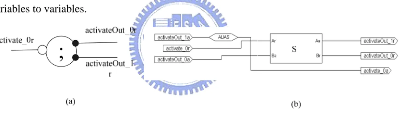
(22) Figure 2-4: The NC2P-element (a) symbol (b) truth table (c) gate-level implementation. Figure 2-5: The S-element (a) symbol (b) gate-level implementation (c) handshaking protocol Figure 2-5 shows the S-element which perform a series of handshake. An S-element has 4 pins including 2 request/acknowledge handshake pairs – ‘Ar’/’Aa’ and ‘Br’/’Ba’. It is composed by nc2p, NOR and AND gates.. 13.
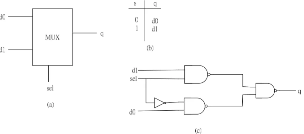
(23) Figure 2-6: The multiplexer (a) function block (b) true table (c) gate level implementation. Figure 2-7: The de-multiplexer (a) function block (b) true table (c) gate level implementation The basic multiplexer and de-multiplexer are shown in figure 2-6 and figure 2-7. They are used in many elements such as Basla full adder and BrzCase.. 2-3-2 Handshake Components There are about 40 handshake components in Balsa. Each handshake components maps to a individual gate level implementation. We will illustrate some 14.
(24) of them.. Figure 2-8: The Fetch Component (a) handshake component (b) gate level implementation Figure 2-8 shows the Fetch component. This component is used to transfer data from input channels to variables, from variables to output channels, and from variables to variables.. Figure 2-9: The Sequence Component (a) handshake component (b) gate level implementation. Figure 2-9 and figure 2-10 are sequence and concurrent component respectively. They control the executing of the components which is sequential or parallel.. 15.
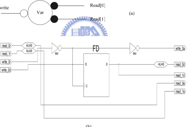
(25) Figure 2-10: The Concurrent Component (a) handshake component (b) gate level implementation. Figure 2-11: The Variable Component (a) handshake component (b) gate level implementation Figure 2-11 shows the variable component. It uses D-type flip-flop to store data. 16.
(26) When we declare variables in out Balsa programs, they will be mapped into variable components. Data is stored when the signal write_0r is set, and read when the signal read_0r or read_1r is set.. 17.
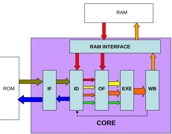
(27) Chapter 3 The Design This chapter describes the decoder design of asynchronous 8051 microprocessor. This decoder is for pipelined 8051 with IF, ID, OF, EXE, and WB stages.. 3-1 The architecture of the pipelined asynchronous 8051 The architecture of asynchronous pipelined 8051 is show in figure 3-1 RAM. RAM INTERFACE. ROM. IF. ID. OF. EXE. WB. CORE. Figure 3-1 The architecture of asynchronous pipelined 8051 There are five stages of our pipeline, and an interface between the processor core and the RAM. The IF (instruction fetch) stage fetches instructions from ROM. The ID (instruction decode) stage decodes the instruction and handles the branch instruction. The OF (operand fetch) stage fetches operands from RAM. The EXE (execute) stage execute instructions according to opcodes of instructions. The WB 18.
(28) (write back) stage write back the result into RAM.. 3-2 The design of IF stage The architecture of the IF stage is show in figure 3-2.. ctrl_2_buf1_addr interface_2_buf1_data. IF_2_ID_data ctrl_2_buf1_RnW. mem_2_IF_data. buffer1 mem. buf1_2_ctrl_data. buf1_2_interface_addr. fetcher ctrl. interface. ctrl_2_buf2_addr. interface_2_buf2_data. ctrl_2_buf2_RnW. buffer2. IF_2_mem_addr. buf2_2_ctrl_data. buf2_2_interface_addr. ID_2_IF_addr. Figure 3-2 The architecture of IF stage There are three basic components in the IF stage- mem interface, buffer, and fetcher ctrl. Mem interface is a arbitrator to arbitrate requests from one of the buffers. Buffers are controlled by fetcher ctrl. According to the control signal, buffers prefetch instructions from the external ROM or provide the target byte which fetcher ctrl needs. Fetcher ctrl receives the value of the program counter, and check if it is hit in one of the buffers or miss. If it is hit, fetcher ctrl sends a request of read to the hit buffer, and if it is miss, fetcher ctrl sends a request of prefetch to all buffers. In addition, if the buffer is read the last byte, fetcher ctrl would send a request of prefetch.. 3-2-1 Mem Interface In asynchronous systems, there exists a problem that the inputs of a merge circuit may come simultaneously. In Balsa, we can use an arbitrator component to solve this problem. The mem interface may receive a address for one of the buffers and access the ROM according to this address. However, it would happen that both buffers send addresses to the mem interface and the circuit might be error. Thus, we use the “arbitrate description” to resolve this problem. 19.
(29) arbitrate buf1_2_interface_addr then interface_2_mem_addr <- buf1_2_interface_addr; direct := 1 |buf2_2_interface_addr then interface_2_mem_addr <- buf2_2_interface_addr; direct := 0 end The mem interface behaves as the flow chart shown in Figure 3-3.. start Arbitrate buf1,buf2 y Buf1?. Buf1 fetch. n. Buf12 fetch. Figure 3-3 the flow chart of the mem interface 3-2-2 Buffers For each buffer, it receives the target address and the action signal from fetcher ctrl. If the action signal is read, it returns the target byte according to the address. If the action signal is write, it fetches 32 byte data which start from the address. The buffer behaves as the flow chart shown in Figure 3-4.. 20.
(30) start Get action and address. Read?. Return data. Fetch 32 bytes data. Figure 3-4 the flow chart of the buffer 3-2-3 Fetcher Ctrl Fetcher ctrl controls all the buffers. It fetches the value of the program counter first. Then it checks if the target byte exists in one of the buffers. If there is a buffer which has the byte, Fetcher ctrl sends a read request and the address to the buffer and then passes the target byte to the ID stage. If the target byte is the last byte of the buffer, fetcher ctrl will send a write request to the buffer. However, if no buffer has the target byte, fetcher ctrl will flush all the buffers. The behavior of fetcher ctrl is shown in Figure 3-5.. start Get PC y. n In Buf1?. Return data. y. Return data Check end. Check end. In Buf2?. n. Fill buffer. Return data. Figure 3-5 the flow chart of the fetcher ctrl 21.
(31) 3-3 The design of ID stage The architecture of the ID stage is show in figure 3-3. The ID stage is divided into ID1 and ID2 two stages. In the ID1, it fetches the first byte of an instruction, decodes this instruction, determine the remained bytes, abstract the opcode, and generate the control signal of this instruction. In the ID2, it would fetch remained bytes and provide completed control signals for the OF stage. If the current instruction is a branch instruction, the ID2 stage would calculate the target address and handle the branch action. ActionCtrl IF_2_ID_data. jmp ReadOut. ID1. WriteOut. OpcodeOut. ReadIn. ID2. WriteIn. Opcodein. ID_2_IF_addr. Figure 3-6 The architecture of ID stage 3-3-1 The ID1 stage When ID1 receives the instruction byte, it would determine that this instruction is regular or non-regular. This could decrease the size of the multiplexer. Then, according to the instruction, ID1 generates the signals needed by the following stages such as the remained bytes, the opcode, the read signal, and the write signal. In order to decrease the area cost, we use the shared procedure in Balsa, which would construct only one component whatever times this procedure is called. The example description of the shared procedure is shown in the below. shared readMEMB is 22.
(32) begin read_data.ctrl := MEMB end The behavior of the ID1 stage is shown in Figure 3-7.. start Get instruction. Check regular. Regular?. Regular case. Irregular case. Send control signals. Figure 3-7 The flow chart of the ID1 stage 3-3-2 The ID2 stage In the ID2 stage, it will fetch the remained bytes first. To avoid the race condition between the ID1 stage and ID2 stage, we use the “handshake enclosure” description in Balsa to promise that ID2 fetches the remained bytes before ID1 fetches a new instruction. The handshake enclosure is shown in the below. ActionCtrl -> then case ActionCtrl of … end After fetches all remained bytes, ID2 would transform these bytes into suitable operands and pass all signals to the OF stage. If the instruction is a branch instruction, ID2 would calculate the target address and change the PC value if the branch is taken. The behavior of the ID2 stage is shown in Figure 3-8.. 23.
(33) start Case ActionCt rl of?. 0 remained byte. 1 remained byte. Fetches 1 byte. 2 remained byte. Fetches 2 byte. Branch instruction. Handle branch. Pass the control signal. Figure 3-8 The flow chart of the ID2 stage. 24.
(34) Chapter 4 Implementation and Verification We will show the design flow of implementations and the simulation in this chapter. Because this project is cooperated with the pipelined asynchronous 8051, we will simply illustrate the hole design with the pipelined asynchronous 8051.. 4-1 The design flow of FPGA We had already implemented an asynchronous pipelined 8051 with Balsa. The Balsa program was compiled into a handshake component netlist, and finally this netlist was converted to a verilog gate-level netlist for Xilinx FPGA. With the gate-level netlist, we used other CAD tool to implement this circuit and do some simulation. Because we wanted to implement the circuit in Xilinx FPGA, first we got the gate-level netlist by Balsa. Second, we imported this netlist into Xilinx ISE, a CAD tool for Xilinx FPGA. Then we added "keep hierarchy" description for each handshake component to avoid the optimization of CAD tool because the optimization will break the timing constraint. Finally we followed the standard design flow of the Xilinx FPGA, and burned the design into FPGA. All the flow is shown in Figure 4-1. 25.
(35) .. Figure 4-1. The FPGA design flow. 4-2 Verification We can do behavior simulation for PA8051 (pipelined asynchronous 8051) in Balsa. The simulation environment is shown in figure 4-2. 26.
(36) In Balsa environment, we can use Balsa memory module to avoid duplicate calls of memory, which would construct duplicate memory modules. Figure 4-3 shows the memory module. We can write instructions into memory module, and then executing CPU core and memory parallelly. When all instructions have been executed, we can compare the result in the output ports with the result made bye 8051 simulator. If the results are not in the output ports, we should add some instructions to move the results from RAM to output port.. P0 ~ P3. Rom data. Rom address. PA8051(BALSA). Figure 4-2: PA8051 simulation environment. 27.
(37) Figure 4-3. The ROM model. 28.
(38) Chapter 5 The Result 5-1 Simulation result We have successfully completed the behavior simulation in Balsa with small benchmarks such as GCD and Fibnacci Code. The simulation results are shown in the following.. 5-1-1 The performance of the decoder Because we integrate a cache-like buffer with our decoder, we need to know the effects with different kinds of buffers. We first measured the issue rate with different numbers of buffers. The buffer size is 32 bytes, and because the programs of GCD or Fibnacci Code are small, the benchmark is 256 instruction of the additions. The result is shown in table 5-1. The consumed time The numbers of buffers. The normalized result (in Balsa units). 0. 155,062,000. 20.55. 1. 11,896,100. 1.58. 2. 7,544,200. 1. 3. 10,012,600. 1.33. Table 5-1. The comparison of different numbers of buffers. Second, we measured the issue rate in different sizes of buffers. The buffer size are 8 bytes, 16 bytes, 32 bytes and 64 bytes. The result is shown in table 5-2.. 29.
(39) The size of buffer. The consumed time. (byte). (in Balsa units). 8. 7,801,000. 1.03. 16. 7,629,800. 1.01. 32. 7,544,200. 1. 64. 7,501,400. 0.99. The normalized result. Table 5-2. The comparison of different sizes of buffers. Finally, we measured the performance of the whole pipelined asynchronous 8051 with different sizes of the buffer. The result is shown in table 5-3. The size of buffer. The consumed time The normalized result. (byte). (in Balsa units). 8. 13,681,400. 1. 16. 13,681,400. 1. 32. 13,681,400. 1. 64. 13,681,400. 1. Table 5-3. The performance of the whole pipelined asynchronous 8051 with different sizes of buffers. 5-1-2 The performance of the pipelined asynchronous 8051 The comparison of performance and cost of single-cycle asynchronous 8051 and pipelined 8051 is shown in Figure 5-1. We use the pipelined asynchronous 8051 with two 32-byte buffers to compare with the single-cycle 8051, 30.
(40) SA8051[2], which was designed by our laboratory last year. The consumed time (in Balsa unit). The normalized time. (in Balsa unit). The normalized cost. SA8051. 24,891,300. 3.30. 210,513.5. 0.43. PA8051. 7,544,200. 1. 494,752.25. 1. The cost. Table 5-4. The comparison between the 1-cycle asynchronous 8051 and the pipelined asynchronous 8051 5-2 Area cost We use the Xilinx ISE 6.3i to synthesize our PA8051 processor, and the target FPGA chip is Xilinx FPGA Spartan-IIE 300 ft256. The gate count and path delay are shown in Table 5-1. The gate and path delays of every part of PA8051 are shown in table 7. The ID stage is the most dominant stage of the whole design, taking half of the total cost of PA8051. The biggest part is the ID stage. That is because that there are 256 cases of instructions. Even though we divided the instructions into regular and non-regular instructions, they still need to be multiplexed and that causes the cost so big.. 31.
(41) Slice. gate. minimum path delay(ns). IF. 1007. 13987. 757. ID. 5353. 61973. 721. OF. 564. 7086. 34. EXE. 1284. 16938. 174. MEM_INTERFACE. 1098. 13217. 125. RAM_READ_ARBITOR. 57. 1051. 28. WB. 232. 2977. 40. TOTAL. 9595. 117229. Table 5-5. The Cost of Every Part of 8051. 5-3 The discussion of the result Through the comparison of the different numbers of buffers, we can easily find out that if there is no buffer, the delay of the memory access is huge. If there is only one buffer, it saves the memory access time. However, if there are two buffers, it not only saves the memory access time but also hides some accesses when the instructions are executed. If there are three buffers, the additional buffer doesn’t give any new contribution and the issue rate is lower. Furthermore, with the comparisons of the different buffer sizes, the simulation results show that if the buffer size increases, the consumed time decreases slightly. Because the benchmark is a simple 256-addition operation without any branch instruction, the locality is not outstanding. If we consider the benchmark program of GCD or Fibnacci Code, the 32-byte buffer design is enough. With the comparison of the performance of the whole pipelined asynchronous 8051, we got an unexpected result. The performances of different buffer sizes are the same. That is because that the memory in balsa is not a synthesizable component but is an emulation module, and hence the speed of the memory overtakes the pipeline of speed of the PA8051. If we want to obtain the 32.
(42) actual performance, we need to implement the whole design in the gate-level or other physical levels. Finally, with the comparison of the single cycle asynchronous 8051 and the pipelined asynchronous 8051, we can see that although the area cost become two times, the performance is increased to three times.. 33.
(43) Chapter 6 Conclusions and Future Works In this thesis, we proposed a new decoder design of asynchronous pipelined 8051 microprocessor. We have confirmed its correctness and implemented it in Xilinx FPGA. Although it area may be a little large, it performance has been improved. The contributions of this thesis is : z. The novel decoder for our pipelined asynchronous 8051 has been developed.. z. The design flow of using CAD tool to design an asynchronous system is confirmed.. The future works which we can do are : z. Optimizing the Balsa code to reduce the area cost.. z. Completing the layout simulation and realizing our design with CMOS chips.. 34.
(44) Reference [1]. A. Bardsley, D. A. Edwards, “The Balsa Asynchronous Circuit Synthesis. [2]. System” Yuan-Teng Chang, “SA8051: An Asynchronous Soft-core Processor for. [3]. Low-Power System-on-Chip Applications”, 2005. Cota, E.F.; Krug, M.R.; Lubaszewski, M.; Carro, L.; Susin, A.A,. [4]. “Implementing a self-testing 8051 microprocessor”, Integrated Circuits and Systems Design, 1999. Proceedings. XII Symposium on 29 Sept.-2 Oct. 1999 Page(s):202 - 205 van Gageldonk, H.; van Berkel, K.; Peeters, A.; Baumann, D.; Gloor, D.; Stegmann, G.;” An asynchronous low-power 80C51 microcontroller”, Advanced Research in Asynchronous Circuits and Systems, 1998. Proceedings. 1998 Fourth International Symposium on , 30 March-2 April 1998 Pages:96 – 107. [5] [6]. Intel, “MCS51 Microprocessor Family User’s Manual: Intel”, 1994 Martin, A.J.; Nystrom, M.; Papadantonakis, K.; Penzes, P.I.; Prakash, P.; Wong, C.G.; Chang, J.; Ko, K.S.; Lee, B.; Ou, E.; Pugh, J.; Talvala, E.-V.; Tong, J.T.; Tura, A, “The Lutonium: a sub-nanojoule asynchronous 8051 microcontroller”, Asynchronous Circuits and Systems, 2003. Proceedings. Ninth International Symposium on 12-15 May 2003 Page(s):14 – 23. [7]. Je-Hoon Lee; Won-Chul Lee; Kyoung-Rok Cho, “A novel asynchronous pipeline architecture for CISC type embedded controller, A8051”, Circuits and Systems, 2002. MWSCAS-2002. The 2002 45th Midwest Symposium on Volume 2, 4-7 Aug. 2002 Page(s):II-675 - II-678 vol.2. [8]. Chelcea, T.; Nowick, S.M.; “Resynthesis and peephole transformations for the optimization of large-scale asynchronous systems”, Design Automation Conference, 2002. Proceedings. 39th , 10-14 June 2002 Pages:405 – 410. 35.
(45)
數據
+7
Outline
相關文件
In this section, we consider a solution of the Ricci flow starting from a compact manifold of dimension n 12 with positive isotropic curvature.. Our goal is to establish an analogue
For example Competition Provisions in Hong Kong Chapter 106 Telecommunication Ordinances 7K : S.1 A licensee (entity) shall not engage in conduct which, in the opinion of
We have been promoting STEM education among schools in a holistic and coherent manner, with strategies that embrace renewing the curricula of the Science,
In this chapter we develop the Lanczos method, a technique that is applicable to large sparse, symmetric eigenproblems.. The method involves tridiagonalizing the given
The 3SEQ maximum descent statistic describes clus tering patterns in sequences of binary outcomes, a nd is therefore not confined to recombination analy sis... New Applications (1)
To convert a string containing floating-point digits to its floating-point value, use the static parseDouble method of the Double class..
In this chapter, a dynamic voltage communication scheduling technique (DVC) is proposed to provide efficient schedules and better power consumption for GEN_BLOCK
In this chapter, the results for each research question based on the data analysis were presented and discussed, including (a) the selection criteria on evaluating
