IEEE ELECTRON DEVICE LETTERS, VOL. 32, NO. 3, MARCH 2011 381
Arsenic-Implanted HfON Charge-Trapping
Flash Memory With Large Memory
Window and Good Retention
C. Y. Tsai, T. H. Lee, and Albert Chin, Fellow, IEEE
Abstract—We have fabricated the TaN–[SiO2−LaAlO3]–
HfON–[LaAlO3−SiO2]–Si charge-trapping Flash device. A large
6.4-V initial memory window, a 4.3-V 10-year extrapolated reten-tion window at 125◦C, and a 5.5-V endurance window at 106
cycles were measured under very fast 100-μs and low ±16-V program/erase. These excellent results were achieved using an As+ implant into the HfON trapping layer, which were sig-nificantly better than those of the control device without ion implantation.
Index Terms—Charge-trapping Flash (CTF), HfON, ion
implant, nonvolatile memory (NVM).
I. INTRODUCTION
T
HE metal–oxide–nitride–oxide–Si (MONOS) charge-trapping (CT) Flash (CTF) devices [1]–[15] have been used for the next-generation nonvolatile memory (NVM) be-yond the conventional poly-Si floating-gate Flash memory. This is due to the discrete trapping property of Si3N4that allows the use of a thinner tunnel oxide to improve the erase saturation. However, the much shallower trap energy in Si3N4[11] than the deep 3.15 eV in conventional poly-Si floating gates degrades the high-temperature retention characteristics [12]–[15]. The retention can be improved by using a thicker tunnel oxide, but this yields slow erase (10–100 ms). Such a retention and erase-speed tradeoff is a basic limitation of NVM. Furthermore, both a good memory window and a good endurance should be achieved simultaneously. However, a 10× degradation in endurance is the other limitation for highly scaled CTF memory devices [1] due to the smaller number of electrons stored in the Flash cell.To address these issues, we previously presented Al(Ga)N or HfON layers with deep trap energies as the trapping layer in MONOS CTF devices [12]–[15]. The better retention of high-κ Al(Ga)N MONOS CTF was confirmed by another group [16] and is listed in ITRS [1]. However, the trapping property of HfON is inferior compared to that of Si3N4which can be seen
Manuscript received October 2, 2010; revised November 24, 2010; accepted December 3, 2010. Date of publication January 20, 2011; date of current version February 23, 2011. This work was supported by the National Science Council of Taiwan. The review of this letter was arranged by Editor T. San.
The authors are with the Department of Electronics Engineering and Institute of Electronics, National Chiao Tung University, Hsinchu 300, Taiwan (e-mail: [email protected]).
Color versions of one or more of the figures in this letter are available online at http://ieeexplore.ieee.org.
Digital Object Identifier 10.1109/LED.2010.2100019
in a reduced memory window [14], [15]. In this letter, we report a CTF device with an initial 6.4-V memory window, a large extrapolated ten-year retention window of 4.3 V at 125◦C, and 106endurance under fast 100-μs and low±16-V program/erase (P/E). These excellent results were achieved using an As+ implant into the HfON trapping layer and show significant im-provement compared to the control device without the implant.
II. EXPERIMENTS
The TaN–[SiO2−LaAlO3]–HfON–[LaAlO3−SiO2]–Si de-vices were made by growing the double tunnel oxide layers of 2.5-nm thermal SiO2 on a standard p-Si substrate and 2.5-nm LaAlO3deposited by physical vapor deposition (PVD). Then, the 30-nm HfON was grown by reactive PVD as the CT layer that gives a small 8.4-nm equivalent Si3N4thickness (ENT). The As+implantation into HfON was applied at 10 keV, 1× 1015cm−2dose, and 60◦ titled angle followed by 950◦C 1-s rapid thermal annealing (RTA). Next, 8-nm LaAlO3 was deposited by PVD, and a 7-nm TEOS (Si(C2H5O)4) oxide was deposited by chemical vapor deposition to form the double blocking dielectric layers. Finally, 200-nm TaN was deposited by PVD, followed by gate definition, reactive ion etching, self-aligned 25-keV As+implantation at 5× 1015cm−2 dose, and 900 ◦C 30-s RTA to activate the dopant at the source–drain region. The capacitor size is 100 μm× 100 μm and is isolated by a field oxide. The CTF device has the same layout as that of a MOSFET with a 10-μm gate length and a 100-μm width and is isolated by a field oxide.
III. RESULTS ANDDISCUSSION
Fig. 1 shows the C–V hysteresis of HfON CT stack ca-pacitors with and without the As+ implantation. The C–V hysteresis window increases with increasing voltage, indicating the good trapping property. A large C–V hysteresis window of 11.1 V was obtained in As+-implanted CT stack capacitors under±16-V sweep. The large hysteresis window is not due to device variations, as evident from the close capacitance density in control devices. The large increase in the hysteresis window may be due to the forming deep energy levels [17] in the HfON trapping layer by the As+implant with 950◦C RTA.
Fig. 2 shows the Jg–Vgcharacteristics of the HfON MONOS
CTF devices with and without the As+ implant. The Jg–Vg
was measured at a sweep rate of 2.5 V/s. The gate leakage current obtained on As+-implanted devices is close to that on
382 IEEE ELECTRON DEVICE LETTERS, VOL. 32, NO. 3, MARCH 2011
Fig. 1. C–V hysteresis of HfON CT stack capacitors with and without As+
implant.
Fig. 2. Jg–Vgcurves of HfON MONOS CTF devices with and without As+
implant.
the control devices, indicating that the 60-tilted and 10-keV As+ implant did not reach or damage the tunnel oxide layers. The slightly lower leakage current in As+-implanted devices at high Vg is related to the better electron trapping efficiency
shown in Fig. 1, which results in an increased effective barrier height by Columbic repulsive force.
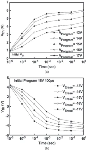
Fig. 3(a) and (b) shows the program and erase characteristics of As+-implanted HfON CTF devices. The threshold voltage (Vth) increases with increasing P/E voltage and time with a small saturation effect. At±16-V and fast 100-μs P/E, a large ΔVth memory window of 6.4 V is obtained. Such a large memory window is even better than that of the Si3N4–HfON double-trapping-layer CTF device [15]. The fast 100-μs P/E speed is due to the additional conduction and valance band discontinuity (ΔEC and ΔEV) in LaAlO3 and SiO2 barriers for easier tunneling during program and erase, respectively.
Fig. 4(a) and (b) shows the retention and endurance characteristics. For As+-implanted HfON devices at ±16-V and 100-μs P/E, large ten-year extrapolated memory windows of 5.1 and 4.3 V were obtained at 25 ◦C and 125 ◦C, respectively, which are better than the retention window of control devices. The good retention is due to the physically thicker double LaAlO3−SiO2 for carrier confinement, while the ΔECand ΔEV in LaAlO3/SiO2improve the program and erase speed. This large ten-year retention window with a small
Fig. 3. (a) Program and (b) erase characteristics of As+-implanted HfON
MONOS CTF devices for different voltages and times. For erase, the device was initially programmed at 16 V for 100 μs.
8.4-nm ENT trapping layer allows multilevel cell storage even at 125◦C [15].
At the same±16-V and 100-μs P/E condition, the control device without the As+ implant shows significantly smaller initial and ten-year retention memory windows. The control de-vice can also be programmed to reach a larger memory window at±18-V and 100-μs P/E, but the retention characteristics are slightly inferior to those of the As+-implanted device. This may be due to the generation of deep levels [17] in the trapping layer due to the As+ implantation. Additionally, the control device can only be cycled up to 105cycles at±18-V and 100-μs P/E pulse duration, which is a typical value for CTF memory cells. In sharp contrast, the As+-implanted device has 10× better endurance with a large 106cycled window of 5.5 V at±16-V and 100-μs P/E. This excellent 106 cycling is vital to allow further endurance improvement in highly scaled CTF devices with fewer electrons. Such good endurance is due to the high CT efficiency, allowing low P/E voltage, fast 100-μs P/E speed, and the existing ΔEC and ΔEV for easy tunneling that leads
to less stress in the LaAlO3−SiO2tunnel oxide.
IV. CONCLUSION
Using As+ implantation into the HfON trapping layer of the MONOS CTF device, a large 6.4-V initial memory window, a 4.3-V 10-year extrapolated retention window at
TSAI et al.: ARSENIC-IMPLANTED HfON CTF MEMORY WITH LARGE MEMORY WINDOW AND GOOD RETENTION 383
Fig. 4. (a) Retention and (b) cycling characteristics of HfON MONOS CTF devices with and without As+implant.
125◦C, and a 5.5-V endurance window at 106cycles have been demonstrated under a fast 100-μs speed and a low P/E voltage of±16 V.
REFERENCES
[1] The International Technology Roadmap for Semiconductors (ITRS), 2009. [Online]. Available: www.itrs.net
[2] S.-I. Minami and Y. Kamigaki, “A novel MONOS nonvolatile memory device ensuring 10-year data retention after 10 erase/write cycles,” IEEE Trans. Electron Devices, vol. 40, no. 11, pp. 2011–2017, Nov. 1993. [3] M. H. White, Y. Yang, A. Purwar, and M. L. French, “A low voltage
SONOS nonvolatile semiconductor memory technology,” IEEE Trans. Compon., Packag., Manuf. Technol. A, vol. 20, no. 2, pp. 190–195, Jun. 1997.
[4] M. She, H. Takeuchi, and T.-J. King, “Improved SONOS-type Flash mem-ory using HfO as trapping layer,” in Proc. IEEE Nonvolatile Semicond. Memory Workshop, 2003, pp. 53–55.
[5] C. H. Lee, K. I. Choi, M. K. Cho, Y. H. Song, K. C. Park, and K. Kim, “A novel SONOS structure of SiO2/SiN/Al2O3with TaN metal
gate for multi-giga bit Flash memories,” in IEDM Tech. Dig., 2003, pp. 613–616.
[6] C. W. Oh, S. D. Suk, Y. K. Lee, S. K. Sung, J.-D. Choe, S.-Y. Lee, D. U. Choi, K. H. Yeo, M. S. Kim, S.-M. Kim, M. Li, S. H. Kim, E.-J. Yoon, D.-W. Kim, D. Park, K. Kim, and B.-I. Ryu, “Damascence gate FinFET SONOS memory implemented on bulk silicon wafer,” in IEDM Tech. Dig., 2004, pp. 893–896.
[7] M. Specht, R. Kommling, L. Dreeskornfeld, W. Weber, F. Hofmann, D. Alvarez, J. Kretz, R. J. Luyken, W. Rosner, H. Reisinger, E. Landgraf, T. Schulz, J. Hartwich, M. Stadele, V. Klandievski, E. Hartmann, and L. Risch, “Sub-40 nm tri-gate charge trapping nonvolatile memory cells for high-density applications,” in VLSI Symp. Tech. Dig., 2004, pp. 244–245.
[8] X. Wang, J. Liu, W. Bai, and D.-L. Kwong, “A novel MONOS-type nonvolatile memory using high- κ dielectrics for improved data retention and programming speed,” IEEE Trans. Electron Devices, vol. 51, no. 4, pp. 597–602, Apr. 2004.
[9] Y. N. Tan, W. K. Chim, W. K. Choi, M. S. Joo, T. H. Ng, and B. J. Cho, “High- κ HfAlO charge trapping layer in SONOS-type non-volatile memory device for high speed operation,” in IEDM Tech. Dig., 2004, pp. 889–892.
[10] X. Wang and D.-L. Kwong, “A novel high- κ SONOS memory using TaN/Al2O3/Ta2O5/HfO2/Si structure for fast speed and long retention
operation,” IEEE Trans. Electron Devices, vol. 53, no. 1, pp. 78–82, Jan. 2006.
[11] S. H. Gu, T. Wang, W. P. Lu, Y. H. Ku, and C. Y. Lu, “Extrac-tion of nitride trap density from stress induced leakage current in silicon–oxide–nitride–oxide–silicon Flash memory,” Appl. Phys. Lett., vol. 89, no. 16, pp. 163 514–163 516, Oct. 2006.
[12] C. H. Lai, A. Chin, K. C. Chiang, W. J. Yoo, C. F. Cheng, S. P. McAlister, C. C. Chi, and P. Wu, “Novel SiO2/AlN/HfAlO/IrO2memory with fast
erase, large ΔVthand good retention,” in VLSI Symp. Tech. Dig., 2005,
pp. 210–211.
[13] A. Chin, C. C. Laio, K. C. Chiang, D. S. Yu, W. J. Yoo, G. S. Samudra, S. P. McAlister, and C. C. Chi, “Low voltage high speed SiO2/AlGaN/AlLaO3/TaN memory with good retention,” in IEDM
Tech. Dig., 2005, pp. 165–168.
[14] C. H. Lai, A. Chin, H. L. Kao, K. M. Chen, M. Hong, J. Kwo, and C. C. Chi, “Very low voltage SiO2/HfON/HfAlO/TaN memory
with fast speed and good retention,” in VLSI Symp. Tech. Dig., 2006, pp. 54–55.
[15] S. H. Lin, A. Chin, F. S. Yeh, and S. P. McAlister, “Good 150◦C retention and fast erase charge-trapping-engineered memory with scaled Si3N4,” in
IEDM Tech. Dig., 2008, pp. 843–846.
[16] K. H. Joo, C. R. Moon, S. N. Lee, X. Wang, J. K. Yang, I. S. Yeo, D. Lee, O. Nam, U. I. Chung, J. T. Moon, and B. I. Ryu, “Novel charge trap devices with NCBO trap layers for NVM or image sensor,” in IEDM Tech. Dig., 2006, pp. 979–982.
[17] M. C. Kim, S. H. Hong, H. R. Kim, S. Kim, S.-H. Choi, R. G. Elliman, and S. P. Russo, “Nonvolatile memories using deep traps formed in Al2O3
by metal ion implantation,” Appl. Phys. Lett., vol. 94, no. 11, pp. 112 110-1–112 110-3, Mar. 2009.