i
單晶片網路系統的階層式架構
研究生 : 林 煌 凱
指導教授 : 周 景 揚 博士
國 立 交 通 大 學
電 子 工 程 學 系 電 子 研 究 所 碩 士 班
摘 要
隨著半導體製程的進步,在未來十年後將有可能實現單一晶片上整合上百個運算 元件。屆時,各元件之間的通訊將會是影響系統效能的一大關鍵。IC 設計工程師 需要一個能考慮通訊效能的系統設計方法。在這篇論文中,改良傳統二維網狀單晶 片網路系統平台而提出階層式架構。此架構用以支援幾百個任務的複雜度或擁有大 量資料傳輸的應用。此外,藉由考慮傳輸資料量、資料傳輸衝突和頻寬設限損失的 任務結合方法來達到新架構的整體系統效能的提升。並在系統層級模擬單晶片網路 系統的資料傳輸行為以預測整體系統效能。建立一自動化的單晶片網路系統效能模 擬工具,IC 設計工程師在系統層級得藉此工具預測所設計平台的效能且得到所設 計平台的設計參數,補足自應用階段至 RTL 階段的設計斷層,以節省所需的設計時 間和成本。ii
Hierarchical Architecture for
Network-on-Chip Platform
Student : Huang-Kai Lin Advisor : Dr. Jing-Yang Jou
Department of Electronics Engineering
Institute of Electronics
National Chiao Tung University
ABSTRACT
As the advance of semiconductor technology, it is possible to integrate hundreds of processing elements on a single chip in the next decade. When the time comes, communication between the components will be the critical factor for system performance. IC designers need a communication-driven system design methodology. In this thesis, improving the traditional 2-D mesh Network-on-Chip (NoC) platform by the hierarchical architecture is proposed. The hierarchical architecture is used to support applications with the complexity of several hundreds of tasks or with large amount of transmission data. Besides, applying the task binding method by
iii
considering communication amount, communication data contention and bandwidth penalty to achieve the system overall performance improvement of the new architecture. Modeling the NoC system data transmission behavior at system level is applied to predict system overall performance. Then, an automatic NoC system performance simulation tool is built. Therefore, IC designers can predict the system performance and get all parameters of designed platform at system level. That will make up the design gap between the application level and RTL level to reduce the design time and the design cost.
iv
Acknowledgements
First of all, I would like to express my genuine appreciation to my advisor Professor Jing-Yang Jou for his guidance and instruction during my master studying. Then, I would also like to give my gratitude to my co-guidance advisor Professor Lan-Da Van for his suggestions. I have the honor of being their student very much. Also, I would be indebted to Cheng-Yeh Wang, Liang-Yu Lin, Zwei-Mei Lee, Pao-Jui Huang, and Chen-Ling Chou for their great help on my research and getting so much knowledge from them. Specially thanks to all members of EDA lab for their friendship. Finally, I would show my gratitude to my family and all my friends for their encouragement.
v
Contents
摘要………i Abstract………..ii Acknowledgements………...iv Contents………..v Lists of Tables………..vii Lists of Figures………viii Chapter 1 Introduction ... 1 1.1 Technology Trend ... 11.2 Communication-Driven System Design Methodology ... 3
1.3 Relative Work ... 4
1.4 Motivation ... 4
1.5 Thesis Organization... 6
Chapter 2 Overview of Network-on-Chip... 7
2.1 Network-on-Chip Platform... 7
2.2 Switch ... 9
2.2.1 Switching Strategy... 9
2.2.2 Virtual-Circuit Switching ... 12
2.2.3 Switch Architecture ... 18
vi 3.1 Hierarchical Architecture... 22 3.2 Problem Formulation... 27 3.3 Design Methodology ... 30 3.4 Task Mapping ... 31 3.4.1 Cost Function... 31 3.4.2 Simulated Annealing ... 32
3.5 Connection Path Assignment... 33
3.5.1 Routing Resource Graph ... 33
3.5.2 Cost Function... 37
3.5.3 The Path Assignment Algorithm Considering Contention ... 40
Chapter 4 Experimental results ... 47
4.1 Experimental Flow ... 48
4.2 Experimental Results... 51
4.2.1 Hierarchical Bandwidth Scalability Analysis... 51
4.2.2 Performance Analysis... 53
4.2.3 Task Graph Complexity Analysis ... 60
vii
List of Tables
Table 4.1: Comparison between traditional and hierarchical architecture at communication factor = 4 and buffer size = 2... 60
viii
List of Figures
Figure 1.1: Communication-driven system design methodology... 3
Figure 2.1: 2-D mesh topology network... 8
Figure 2.2: Example of packet switching. ... 10
Figure 2.3: Illustration of communication deadlock. ... 11
Figure 2.4: Example of virtual channel scheme. ... 13
Figure 2.5: Request-oriented weighted round-robin scheduling scheme. ... 14
Figure 2.6: Data transmission from a switch to the adjacent switch or the local processor. ... 15
Figure 2.7: Switch buffer organization... 16
Figure 2.8: Switch architecture... 18
Figure 2.9: Expression of the buffer-id... 19
Figure 3.1: Hierarchical 2-D mesh NoC platform... 22
Figure 3.2: Data transmission between two L2 switches. ... 23
Figure 3.3: Example of data transmission passing through hierarchy... 25
Figure 3.4: Buffer architecture of SW_1I... 25
Figure 3.5: Buffer architecture of SW_I... 26
Figure 3.6: Task graph of MPEG-4 encoder... 27
Figure 3.7: Example of task binding problem. ... 29
Figure 3.8: Design methodology. ... 30
ix
Figure 3.10: Routing resource graph between PE and local switch. ... 34
Figure 3.11: Routing resource graph of a switch... 35
Figure 3.12: Routing resource graph across a physical channel. ... 36
Figure 3.13: Contention occurrence in time domain. ... 38
Figure 3.14: Procedure of connection path assignment algorithm. ... 40
Figure 3.15: Pseudo-code of the Pathfinder algorithm... 41
Figure 3.16: Example of solving overuse problem. ... 43
Figure 3.17: Solution of overuse problem... 44
Figure 3.18: Solution of optimizing contention... 45
Figure 4.1: Experimental environment mapping to design methodology. ... 48
Figure 4.2: Experimental environment... 50
Figure 4.3: Latency versus different R. ... 51
Figure 4.4: Throughput versus different R. ... 52
Figure 4.5: Fail rate versus different communication factor. ... 54
Figure 4.6: Fail rate versus different buffer size... 55
Figure 4.7: Latency versus different communication factor... 56
Figure 4.8: Latency versus different buffer size... 57
Figure 4.9: Throughput versus different communication factor... 58
Figure 4.10: Network usage versus different communication factor... 59
Figure 4.11: Fail rate versus different task number. ... 61
Figure 4.12: Latency versus different task number. ... 62
x
1
Chapter 1
Introduction
1.1 Technology Trend
As the semiconductor technology advances, it is feasible to integrate multi-billion of transistors on a chip. Hence, hundreds of intellectual properties (IPs) including general propose processors and application specific functional blocks will be integrated onto a single chip. However, designers will encounter several new problems.
First, the ever-shrinking feature size causes the gate delay scaling down linearly, whereas the wire delay remains constant. Hence, the wire delay will become more
2
critical than the gate delay [1]. Though the wire delay can be conquered by wire pipelining techniques, the problem of timing uncertainty is still hard to be dealt with. On the other side, the clock skew can not be neglected any more and clock synchronization becomes another problem for designers. It is almost impossible to synchronize all components on a chip with single clock. The globally-asynchronous, locally synchronous (GALS) technique is the most suitable solution [2] for solving this problem.
Second, traditional shared-bus based network architecture is the most popular architecture in current System-on-Chip (SoC). However, high data transmission contentions between masters reduce the system performance and raise the power consumptions. Moreover, buses only can handle 3 to 10 computation elements and can not scale to higher numbers [3]-[5]. Following the technology trend, communication between computing components becomes the critical factor of system performance. Designers need to search for new communication architecture in place of shared-bus architecture.
Third, system design with integrating more computing components and verification become more complex. The traditional design flow is not sufficient to support the technology trend. The design trend is toward system level design. A communication-driven system design methodology will be applied.
3
1.2 Communication-Driven System Design Methodology
Function Modeling
Architecture Modeling
Mapping and Analysis
Software Implement
Hardware Implement
System Integration
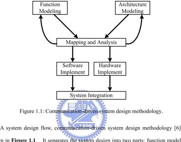
Figure 1.1: Communication-driven system design methodology.
A system design flow, communication-driven system design methodology [6], is shown in Figure 1.1. It separates the system design into two parts: function modeling and architecture modeling. Function modeling contains application modeling, task partition and job scheduling. Architecture modeling contains the simulation models of various computation, memory components and communication fabrics. Designers can make decision to select appropriate platform. In the next step, map and allocate the tasks onto the platform provided by architecture modeling. Designers can get more information of the system and make better design trade-off through performance evaluation. Applying this method, designers can refine the implementation of design at system level and shorten the try-and-error iteration.
4
1.3 Relative Work
The design methodology for communication-based design is proposed in [7]. Researchers in this paper propose a Network-on-Chip (NoC) approach to partition the communication into layers to maximize the reuse and provide programmers with an abstraction of the underlying communication framework. The integrated modeling, simulation and implementation environment are proposed in [8]. NoC infrastructure and processors are modeled, and simulation is performed to find the optimal network configuration. In [9], an algorithm called NMAP which can be applied to both the single-path routing and the spilt-traffic routing to map the cores onto NoC architecture under bandwidth constraints is proposed. A simple packet switching communication model to estimate the communication time and to propose a two-step genetic algorithm to map a parameterized task graph onto the 2-D mesh NoC architecture, which minimizes the overall execution time of the task graph is proposed in [10].
1.4 Motivation
In this world, roads make communication of two far places, for example, footpaths between countries, roads between towns, freeways between cities etc. We can find out that not all roads have the same width because of the different traffic requirement. For example, if all the roads are limited only one-lane, somewhere with heavy traffic is always crowded; if all the roads are assigned four-lane, somewhere without heavy traffic
5
wastes the resource. The freeway is wide and suitable for long distance and large traffic loading. For example, if we want to go to Chu-Pei from Hsin-Chu, we can choose the provincial road or the freeway. If the provincial road is crowded, the freeway is the better choice even the distance of the latter is longer than that of the former. Undoubtedly, the freeway will be chosen if we want to go to Kaohsiung from Taipei, because the freeway is much more unobstructed than any other roads.
To eliminate the communication bottleneck, NoC architecture is used to replace the shared-bus architecture. When the application is complex and the communication loading is heavy, long distance transmission on NoC platform is necessary. If the more complex applications implemented on NoC platform still can not achieve satisfied performance, another new improved architecture should be applied. The conception described above can be used for the communication architecture of the NoC platform. The computing elements can be looked as a city, the communication channels can be looked as provincial roads, and the data flow can be looked as the traffic flow. Therefore, we will add some resource as freeways with large bandwidth to support the complex applications. In this thesis, the hierarchical architecture for 2-D mesh NoC platform is proposed. Moreover, solve the task binding problem to maximum the system performance. Designers can benefit from the proposed framework to analyze the system performance and make decisions at higher design level because of the performance predictable of the platform.
6
1.5 Thesis Organization
In chapter 2, the traditional NoC platform, the switch design considerations and the switch configuration are introduced. Chapter 3 describes the configuration of proposed hierarchical 2-D mesh NoC platform and the communication contention-aware task binding methodology using the platform. The experiment flow and experimental results are shown and discussed in chapter 4. Finally, conclusions and future works are given in the last chapter.
7
Chapter 2
Overview of Network-on-Chip
This chapter will introduce the network-on-chip (NoC) platforms as well as the switch design of on-chip network communications. Switches are the most critical elements for on-chip networks. In this chapter, the common switch strategies, the required switch properties, the switch model, and the transaction behavior will be discussed in more detail.
2.1 Network-on-Chip Platform
8
butterfly fat-tree (BFT), 2-D mesh, etc. which are collated and discussed in [11]. The 2-D mesh topology NoCs have the properties of simple connection and easy routing for communications [12]. Such NoC architectures also have the uniform interconnection and transaction time between two elements, thus ensuring the scalability of the networks. Besides, the rectangular topology of such NoC architectures meets the IC manufacturing topology; in other words, the architectures are easy to be realized. Because of these properties described above, the 2-D mesh topology NoCs are investigated in this work.
SW PE SW PE SW PE SW PE SW PE SW PE SW PE SW PE SW PE
Figure 2.1: 2-D mesh topology network.
Figure 2.1 shows the illustration of 2-D mesh topology networks consisting of
processing elements (PE) and switches (SW). Each PE is composed of a processor with buffers, local memories and network interface, and is used to execute computing jobs. Each PE is also connected to its local switch. This switch can buffer communication data. Each switch connects to the four neighboring switches. The PEs communicate through the switches.
9
2.2 Switch
2.2.1 Switching Strategy
Three widely used switching strategies are connection-oriented switching, connectionless switching, and hybrid switching.
2.2.1.1 Connection-oriented Switching
The connection-oriented switching, named circuit switching, determines a dedicated physical path from the source to the destination before transmitting the data. This dedicated path will be reserved until all the data are transmitted. There are two connection ways of the dedicated paths. The connection ways are determined according to whether the dedicated path can be reprogrammed or not. The static way means that the decided path cannot be reprogrammed, such as point-to-point connection. In contrast, the dynamic way is reprogrammable. If a physical channel is reserved for one dedicated path of data transmission, it is not available for other paths. Such connection ways can have the full bandwidth of the physical channel. This means that the latency will be guaranteed, and the performance is predicable. Hence, the circuit switching is suitable for real-time applications and long, infrequent data transmission. However, one physical channel reserved for only one connection will make the bandwidth utilization low when the transmission is not continuous, and hence this will degrade the overall performance.
10
2.2.1.2 Connectionless Switching
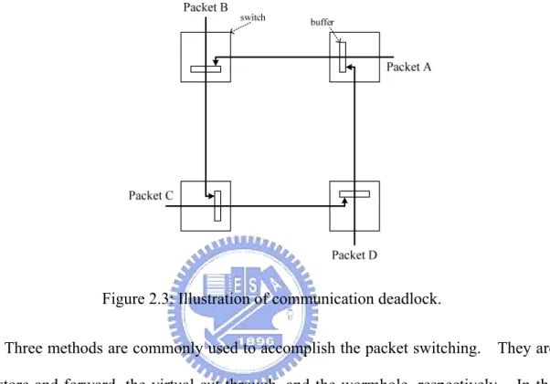
Figure 2.2: Example of packet switching.
In the connectionless switching, named packet switching, the data packets are transmitted. A packet contains the information of the destination, the packet size, and the transmission data. In contrast to the circuit switching, the connection of packet switching from the source to the destination is not reserved before data transmission. For example, a packet will be transmitted from a source PE to a destination PE as shown in Figure 2.2. There are four switches, A, B, C, and D, between the source PE and the destination PE, and there is not only one path to transmit the packet. For the switch A, there are B, C, and D, connected to A. The transmission path is not reserved before the data transmission. When the data is transmitted to A, the next passing switch, B, C, or D, is decided. When utilizing the packet switching, the buffers of a switch are released until the packet is transmitted to the next switch. If there are data buffered in the input or output of a physical channel, other data intending to access this physical channel will be stuck as well until the preceding buffers can be released. In Figure 2.3, no data can be transmitted forward because not any of the front buffers is released. In this example, it is a deadlock situation. In summary, the advantage of the packet switching is that the buffers of packet switching strategies get high utilization. But the latency is
11
unpredictable, because a packet may be blocked for uncertain time when there is heavy traffic.
Figure 2.3: Illustration of communication deadlock.
Three methods are commonly used to accomplish the packet switching. They are the store-and-forward, the virtual-cut-through, and the wormhole, respectively. In the store-and-forward, a packet is allowed to be transmitted to the next switch only when the whole packet is available, and the next switch has the capability of receiving this packet. Hence, the store-and-forward requires large buffer size to provide the capability of a whole packet. Besides, it is efficient for short, frequent transmission. In the virtual-cut-through, a switch can allocate buffers for a whole packet. The packet will be transmitted to the next switch when the routing information is available rather than the whole packet. The latency can be short, and the bandwidth utilization can be high if the routing information is not blocked. However, if the routing information is really
12
blocked, the packet will be completely buffered until it can be transmitted. Summarily, the virtual-cut-through is more efficient than the store-and-forward when considering the latency and the bandwidth utilization. Both of them require large buffer size. In the wormhole switching, a switch only has the capability of some units of a packet instead of a whole packet. It directly transmits data when the next switch has released buffer. Hence, the wormhole switching requires fewer buffers than the store-and-forward and the virtual-cut-through.
2.2.1.3 Hybrid Switching
The hybrid switching means the use of both the circuit switching and the packet switching for different communication requirements in NoC platforms. Therefore, it can have the characteristics of both the circuit and packet switching. The virtual-circuit switching is a hybrid switching when it uses dedicated virtual connections similar to the circuit switching and packet transmission similar to the packet switching.
2.2.2 Virtual-Circuit Switching
In this work, we use a switch architecture which is based on the latency-insensitive concepts [13][14] and utilize the virtual-circuit switching technique. Using the switching architecture can achieve high bandwidth utilization, guaranteed bandwidth and predictable latency under high communication loading. This switching architecture also has predictable characteristics and can support real-time applications.
13
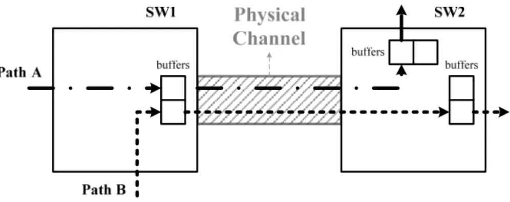
Figure 2.4: Example of virtual channel scheme.
For the virtual channel flow control [15], a physical channel can be divided into several virtual channels. For example as shown in Figure 2.4, both path A and path B try to access the physical channel between SW1 and SW2. Without using the virtual channel scheme, if path A gets the grant of the physical channel first, path B can not access the physical channel until path A finishes transmitting data. The data of the path B will be buffered in the input or output of the physical channel. When applying the virtual channel technique, path A and path B access the physical channel in turns. The waiting time for transmitting the buffered data will be reduced. Thus, the latency will be decreased, the utilization of the channel will be increased, and the system throughput will be improved.
14
Figure 2.5: Request-oriented weighted round-robin scheduling scheme.
In the virtual-circuit switching, the physical channel is divided into several virtual channels. Thus, these virtual channels share the bandwidth of the physical channel. To arrange the available bandwidth of each virtual channel, the request-oriented weighted round-robin scheduling scheme is applied. The round-robin scheduling gives grant sequentially and cyclically, and ignores the buffers without giving request. If a requested buffer has a weight number, w, it can transmit w times continuously as it gets the grant of transmission from the scheduler. The higher weight of the buffer gets the more bandwidth. For example shown in Figure 2.5, Buffer A, B, C and D have weight numbers 1, 2, 2, 1, respectively. The scheduled sequence using the physical channel will be A, B, B, C, C and D. If Buffer A, C and D make requests, Buffer B will be ignored as the sequence index reaches Buffer B in a clock cycle, and Buffer C will get the grant in this clock cycle. As finishing a round, the sequence index will be back to Buffer A. In this case, each Buffer A and D gets one-sixth of the physical channel bandwidth, and each Buffer B and C gets one-third of one.
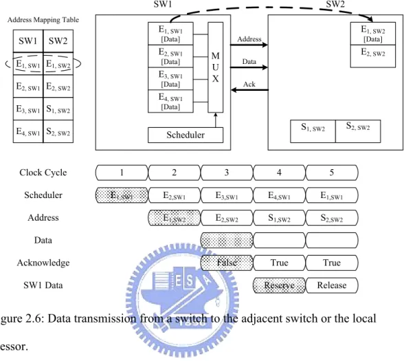
15 E2, SW1 [Data] E1, SW1 [Data] E4, SW1 [Data] E3, SW1 [Data] M U X Scheduler E2, SW2 E1, SW2 [Data] S1, SW2 S2, SW2 Address Data Ack SW1 SW2 SW1 SW2 E1, SW1 E1, SW2 E2, SW1 E2, SW2 E3, SW1 S1, SW2 E4, SW1 S2, SW2
Address Mapping Table
1 2 3 4 5 E1,SW2 False E1,SW1 Reserve Clock Cycle Scheduler Address Data Acknowledge SW1 Data E2,SW1 E3,SW1 S1,SW2 E2,SW2 E1,SW1 E4,SW1 S2,SW2 True True Release Figure 2.6: Data transmission from a switch to the adjacent switch or the local processor.
Figure 2.6 illustrates the data transmission from a switch to an adjacent switch or
to the local processor. The address mapping table in a switch records the destination buffer address of each buffer in this switch. As shown in Figure 2.6, E1, SW1 makes a connection to E1, SW2. If there are data in E1, SW1, they will be transmitted to E1, SW2. The data transmission expends four clock cycles. In the first cycle, the requested buffer E1, SW1 gets the grant from the scheduler, and E1, SW1 can transmit the data in the following cycles. In the second cycle, E1, SW1 sends the destination address of E1, SW2 to SW2 through the Address-line to request SW2 that the transmitted data should be
16
reserved in E1, SW2. In the third cycle, E1, SW2 sends an acknowledge signal back to E1, SW1 through the Ack-line to notify E1, SW1 of the status of E1, SW2. If E1, SW2 is full, the acknowledge signal will be true. On the contrary, if E1, SW2 is available, the acknowledge signal will be false. In the same cycle, E1, SW1 sends the data to E1, SW2 through the Data-line. The transmitted data will be reserved or discarded according to whether E1, SW2 is available or not. In the fourth cycle, the data in E1, SW1 that has been transmitted should be reserved or released according to the acknowledge signal issued from E1, SW2. If the acknowledge signal is false, the data should be reserved and retransmitted in the next round.
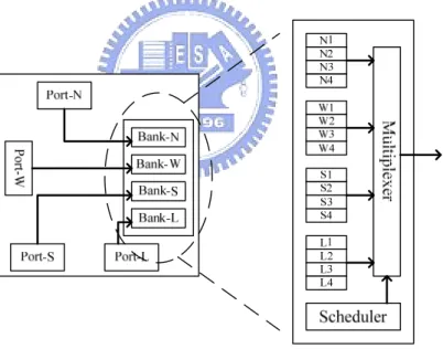
Figure 2.7: Switch buffer organization.
The switch buffer utilization is an important factor for the communication efficiency. Because that sometimes not all the switch buffers are reserved when the number of the connection paths is less than the number of the virtual channels in a
17
physical channel. We use two-port SRAM memories instead of registers to implement the switch buffers. Therefore, we provide the flexibility to make the trade-off between the buffer size and the number of the virtual channels. Figure 2.7 shows an example of the switch buffer organization. There are four buffer banks in a port and each bank only receives data from the corresponding direction. For example, bank-N of E-port only receives data from the input of N-port. Each buffer bank can be divided into several buffer queues to provide necessary virtual channels. As shown in Figure 2.7, a buffer bank is divided into four buffer queues, and there are total sixteen provided virtual channels in a port. Designers can figure out the number of the necessary virtual channels of a buffer bank in the early system design stage and make a suitable switch buffer partition. Taking a 32-word buffer bank for example, it can be divided into 4 8-word buffer queues, 8 4-word buffer queues, or 16 2-word buffer queues for different applications. Thus, this switch buffer organization will make the switch buffer utilization higher, and improve the communication efficiency.
Finally, the switch will assign the dedicated connection paths by reserving the corresponding virtual channels and buffers before the data transmission. The passing switches of connection paths and the communication behavior can be known in early stage of the system design. It means that the switch has predictable characteristics and can support real-time applications.
We utilize the switch architecture with the virtual channel scheme, the request-oriented weighted round-robin scheduling, and SRAM configuration buffers. It
18
has features of deadlock free, high bandwidth utilization, high buffer utilization, and can support real-time applications. Also, it provides capabilities of small latency and high throughput. Comparing to the traditional switching strategies, circuit switching has latency guarantee and can support real-time applications; wormhole switching has smaller buffer size and higher hardware utilization. The virtual-circuit switching has not only the capabilities of circuit switching and wormhole switching but also many other advantages mentioned before.
2.2.3 Switch Architecture
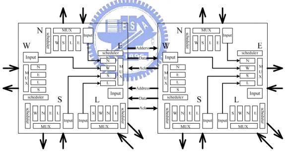
Figure 2.8: Switch architecture.
Figure 2.8 shows the architecture of the proposed switch. There are five ports,
East (E), South (S), West (W), North (N), and Local (L), in a switch. The outputs of the ports, E, S, W and N, are connected to the corresponding input ports of the adjacent
19
switches, and the L port is connected to the interface of the local PE. For example shown in Figure 2.8, the E port output of the left switch is connected to the W port input of the right switch, and two physical channels with different directions, forward and backward, are built across the two switches. Each physical channel includes Address-line, Data-line, and Ack-line. Address-line is used to transmit destination address, Data-line is used to transmit data, and Ack-line is responsible for transmitting the acknowledge signal.
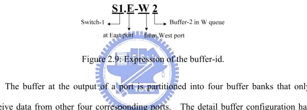
Figure 2.9: Expression of the buffer-id.
The buffer at the output of a port is partitioned into four buffer banks that only receive data from other four corresponding ports. The detail buffer configuration has been shown in Figure 2.7. A switch transmits data to the next switch according to the address in the address mapping table. The expression of the buffer-id is shown in
Figure 2.9. For example, the buffer-id S1.E-W2 means that the buffer belongs to the
second buffer in W-bank of E-port of SW1.
As mentioned in section 2.2.2, a physical channel can be divided into several virtual channels. We use a factor, channel width factor, to indicate the maximum allowable number of the virtual channels in each buffer bank in a port of a switch. For example shown in Figure 2.7, there are four virtual channels in each buffer bank. The
20
channel width factor is four, where a buffer bank can be assigned at most four virtual channels. In other words, there are at most sixteen virtual channels for a physical channel.
The traditional architecture is described in this chapter. However, when the application is complex and the communication loading is heavy, long distance transmission is necessary. We need an improved architecture to support these applications. In the next chapter, the proposed hierarchical architecture will be discussed.
21
Chapter 3
Hierarchical NoC Architecture
In this chapter, the proposed hierarchical architecture for NoC platform is presented, where the task binding method is applied to this platform. Using the hierarchical architecture for complex applications, the overall performance can be improved. The communication contention-aware methodology for the task binding method including task mapping and path assignment is discussed particularly.
22
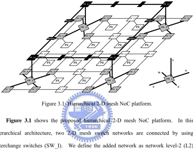
3.1 Hierarchical Architecture
Figure 3.1: Hierarchical 2-D mesh NoC platform.
Figure 3.1 shows the proposed hierarchical 2-D mesh NoC platform. In this
hierarchical architecture, two 2-D mesh switch networks are connected by using interchange switches (SW_I). We define the added network as network level-2 (L2) including SW_I and SW_L2; the traditional part is defined as network level-1 (L1). Every three PEs in x-direction and y-direction, the PE is replaced by SW_I and SW_L2. The port names of a SW_I are shown in Figure 3.1. Some vertical or horizontal physical channels are disconnected in order to release switch ports to connect to SW_I. As shown in Figure 3.1, we assume that the coordinate of a SW_I is (x, y). If the sum of x and y is odd, the horizontal physical channels will be disconnected; if the sum is even, the vertical ones will be disconnected. The buffers between two SW_L2 are relay stations without switches, and they transmit data forward directly in the next clock
23
cycle. A parameter named the physical channel width ratio, R, is used to characterize the hierarchical architecture, and is defined as
L2 L1
Physical channel width Physical channel width
R= (3.1)
The physical channel width means the available size of the transmission data. If the size of L1 transmission data is equal to one-word, and that of L2 data is equal to four-word, R will be given by four.
Figure 3.2: Data transmission between two L2 switches.
In this hierarchical architecture, the data transmission between two L2 switches requires eight clock cycles. The detail timing diagram and the address mapping table of the connections of a SW_L2 are shown in Figure 3.2. This address mapping table
24
records the destination buffer address of each buffer in this switch. In Figure 3.2, the corresponding buffer is labeled in the table. For example, the E1, SW1 buffer has a connection to the E1, SW2 buffer. In the first clock cycle, the requested buffer E1, SW1 gets the grant from the scheduler, and E1, SW1 is allowed to transmit the data in the next cycle. From the second clock cycle to the fourth clock cycle, E1, SW1 sends the address of the destination buffer, E1, SW2, to SW2 through the Address-line. In the fifth clock cycle, the address arrives at SW2, and notifies SW2 that the following data should be reserved in E1, SW2. From the fifth clock cycle to the seventh clock cycle, E1, SW2 sends an acknowledge signal back to E1, SW1 through the Ack-line. At the same clock cycles, E1, SW1 continuously sends three four-word data to E1, SW2 through the Data-line. If E1, SW2 does not have enough buffer space to save the three coming data, the acknowledge signal will be false. On the contrary, if E1, SW2 is available, the acknowledge signal will be true. In the eighth clock cycle, the three data in E1, SW1 that has been transmitted should be reserved or released according to the acknowledge signal received from E1, SW2. If the acknowledge signal is false, this means the transaction is fail, and the data should be reserved and will be transmitted again in the next round. If the acknowledge signal is true, the transaction is succeeded.
25
Figure 3.3: Example of data transmission passing through hierarchy.
For the L1 network, the width of the physical channel is one-word width. On the other hand, for the L2 network, the width is four-word width. Consider an example of a connection path shown in Figure 3.3, the source PE transmits data to the sink PE through L2. A four-word data can be transmitted from SW2 to SW3 when the four one-word data from SW1 is available. SW4 makes transactions to SW5 until the three four-word data from SW3 is available, because a SW_L2 transmits three four-word data continuously. Hence, for the SW_L2 buffers connected to another SW_L2, the weights of the round-robin scheduling are assigned at least three or six.
26
Figure 3.5: Buffer architecture of SW_I.
Since the transmission data size of L2 is four-word, some allocated buffer size should be adjusted. Taking Figure 3.3 for example, if a buffer bank is divided into 16 two-word buffers for SW_L1, we use this queue length, two-word, as a unit. While a buffer receives or sends one four-word data, the queue length should be adjusted to four times the unit. For example, bank-N of S-port of SW2, band-W of L-port of SW3, or bank-W of E-port of SW7, some queue lengths will be adjusted to eight-word. Figure
3.4 shows the buffer architecture of SW7 (SW_1I). The W-port connects to L2, and
the queue length of the buffer banks are all eight-word. Since the bank-W of E-port receives data from L2, the queue length is also eight-word. In other words, in Figure
3.4, Q is the product of q and R. Figure 3.5 shows the buffer architecture of SW3
27
a buffer receives or sends three four-word data, the queue length should be adjusted to twelve times the unit. For example, bank-L of E-port of SW4, or bank-W of L-port of SW5, the queue length will be adjusted to 24-word. The buffer architecture of SW_L2 is similar to Figure 3.4. The queue length of L-port is Q; the queue lengths of other ports are 3Q. The buffer between two SW_L2 is allocated four-word because the buffer is a relay station instead of a switch buffer queue. The large buffer allocation needs a large space and it responds to the discard of the current PE.
3.2 Problem Formulation
Figure 3.6: Task graph of MPEG-4 encoder.
We employ a directed-acyclic task graph to model an application and assume that the application can be partitioned into many communicated tasks due to parallelism. An example shown in Figure 3.6 is a task graph of MPEG-4 encoder [16]. A vertex and an edge denote a task and a data transmission between the tasks, respectively. For example, task C labeled MVMVD performs the motion vector to motion vector difference calculation. After task C is finished, it will transmit C3 unit data to task D. A task can not be executed until the whole computation data is available. For example,
28
task H can not be executed until the C4 unit data from task D and C8 unit data from task G is available.
The task binding problem can be formulated as follows. Given:
1. A directed-acyclic task graph G (V, E) that models an application. For each vertex v ∈ V is defined as a task and the weight is defined as the computation amount. For each directive edge e ∈ E is defined as the data transmission between the tasks and the weight is defined as the communication amount.
2. A NoC platform P (PE, SW) that described before. Goal:
1. To map each task v onto each PE.
2. To assign the communication path between PEs mapping to each edge e. 3. To find the most suitable task mapping and path assignment for maximizing
29 SW SW SW SW Wrapper SW SW Wrapper Wrapper SW SW SW S W X S X T W Y Wrapper T Wrapper Y Wrapper Z Z Task Mapping and Path Assignment A B C D E F G H A B C D E F G H
Figure 3.7: Example of task binding problem.
Figure 3.7 shows an example of the task binding problem and illustrates that the
tasks S, W, X, Y, Z, T are mapped onto PEs and the edges A, B, C, D, E, F, G and H are established as communication paths on the NoC platform. Path A and path D are overlapped, and it means that they will contend in the spatial domain.
30
3.3 Design Methodology
Figure 3.8: Design methodology.
To solve the task binding problem, we use an improved design methodology shown in Figure 3.8. It uses a new cost function that will be described later to obtain a better task binding solution. The NoC platform and the task graph provide the necessary in formation for solving the task binding problem. The task mapping method employs the placement techniques to map each task onto PE. A task is mapped to a PE, so that the number of PEs must be larger than the number of tasks. After task mapping procedure,
31
the connection path assignment method employs the routing techniques to establish the connection paths for the connection edges. Then, the performance analysis is performed to obtain the communication profile in time domain and calculates the contention affected parameters that will be described later. Finally, the feedback mechanism will feed the communication profiles back to the path assignment procedure. The path assignment including the profile information will produce a better path assignment result. The profile referred to as profile-driven optimization provides the more accurate contention information than the system simulation without routing information. The design flow can be proceeded iteratively to enhance the system overall performance.
3.4 Task Mapping
3.4.1 Cost Function
In this work, the goal of task mapping is to minimize the overall communication resource usage. The main idea is that any pair of connected tasks with heavy traffic loading should be allocated as next to each other as possible. A cost function ξ′ is proposed to express the criterion as following.
amount, X pair of processors, X amount, MAX
' D 1 C
C
ξ = × +⎛⎜⎜ ⎞⎟⎟
⎝ ⎠
∑
(3.2)32
destination PE, and the communication amount between a pair of connected processors, respectively. The first term, (D × 1), of the cost function indicates the resource usage of the virtual channels. It is also the conventional cost used in the FPGA placement algorithm. Not only the distance between a pair of connected PE but also the communication amounts between a pair of connected tasks will affect the system performance. The second term, (D × Camount, X / Camount, MAX), of the cost function represents the normalized value that indicates the communication effect of the physical channels, where Camount, MAX is the maximum value of all Camount, X.
3.4.2 Simulated Annealing
Figure 3.9: Example of task mapping.
33
based placers. The task mapping uses the simulated annealing technique because that the technique is simple and suitable for various architectures developed in the on-chip networks. Moreover, it can be easily adapted to different cost requirements for optimization. We take the example of Figure 3.7 as an example of the task mapping shown in Figure 3.9. Assume that the curve of Figure 3.9(b) expresses all the task mapping solutions. At first, map tasks onto PEs randomly as an initial solution, as shown in Figure 3.9(a). Then, a large number of swaps gradually improves the solution and decrease the cost calculated through the cost function list in (3.2), as shown in Figure 3.9(b). Finally, the procedure terminates until finding the local optimal or the global optimal solution, as shown in Figure 3.9(c). Since the detail of simulated annealing is not the focus of this thesis, the detail of the annealing schedule is omitted.
3.5 Connection Path Assignment
3.5.1 Routing Resource Graph
Before describing the connection path assignment procedure, we describe routing resource graph used to represent architecture internally first. In routing resource graph representation, PEs and buffers over virtual channels become nodes; virtual channels become directed edges that indicate data flows unidirectionally. For each node, two factors, capacity and occupancy, denote the maximum number of paths that can use this node and the number of paths currently using this node. Since the NoC platform is represented as a routing resource graph with all possible connections, the path
34
assignment is equivalent to find a path in the routing resource graph starting from a SOURCE node to a SINK node.
Figure 3.10: Routing resource graph between PE and local switch.
Figure 3.10 shows the routing resource graph between a PE and its local switch.
Data flow out from SOURCE node and flow to the OUT node then choose one of the four SW_IN nodes. The label in each SW_IN node indicates that this node will connect to the corresponding SW_OUT node in the local switch; in other words, it denotes the direction that data will flow to. For example, if SW_IN labeled W is chosen, the data will flow to the W port of this local switch. Furthermore, data flow into PE from one of the four SW_OUT nodes that correspond to the four sides of the
35
local switch. Then, data flow into IN node and SINK node, the data transmission is finished.
Figure 3.11: Routing resource graph of a switch.
Figure 3.11 shows the routing resource graph of a switch. It only shows edges
connected to the local port. Each port has four SW_IN nodes that connect to the corresponding SW_OUT nodes of the other four ports. And, each port has four SW_OUT nodes that receive from the corresponding SW_IN nodes of the other four ports. For example, data flow from the local PE, and it can choose to go to any of the adjacent switches; data from any of the adjacent switches can flow into the local PE.
36
Figure 3.12: Routing resource graph across a physical channel.
Figure 3.12 shows the routing resource graph across a physical channel. Only
one direction, right to left in x-direction, is illustrated. Data transmitting from any of the four SW_OUT nodes at W port of the right switch are routed to CHAN_X node. Data then go to any of the four SW_IN nodes at E port of the left switch. If the SW_IN node labeled S is chosen, data will go to the corresponding SW_OUT node at S port of the left switch. In other words, data will flow into the left switch and turn south to the next adjacent switch.
In the routing resource graph, the capacity of each SW_IN and SW_OUT node is set to be equal to the channel width factor that was described in section 2.2.3. If the channel width factor is four, for example, each of these nodes allows at most four connection paths passing through. Since SOURCE, OUT, IN, SINK, CHAN_X, and CHAN_Y nodes all have four different direction data flowing into or out, the capacity of each these nodes should be set four times the channel width factor.
37
3.5.2 Cost Function
The connection path assignment cost function ξ is proposed as following.
data, A A
penalty, A each path, X each channel, A of X amount, MAX
1+N B C ρ ξ = ⎛⎜⎜ + + ⎞⎟⎟ ⎝ ⎠
∑
∑
(3.3)To contrast with (3.2), the distance of the path assignment is the real physical channel number passed by rather than the Manhattan distance used in the task mapping. Furthermore, the transmission data number Ndata, A, the contention factor ρA and bandwidth penalty Bpenalty, A are included to describe the transmission data number of a path through a physical channel, the total effect of communication contention on a physical channel and the bandwidth constraint of a physical channel introduced by other paths.
The detailed expression of Ndata, A, ρA and Bpenalty, A are revealed in the following.
amount, X data, A amount, X , if A L1 , if A L2 C N C R ∈ ⎧ ⎪ = ⎨ ∈ ⎪⎩ (3.4)
where Camount, X is the communication amount of a path X; R is the physical channel width ratio described in section 3.1. Because of the difference between the physical channel width of L1 and that of L2, transmission data number of a physical channel is calculated according to whether this physical channel belongs to.
38 ( , )x y overlap (2 1) (6 5) t = t −t + t −t 2 1 6 5 3 1 6 4 ( ) ( ) ( ) ( ) Y X t t t t t t t t → − + − Γ = − + − , X Ndata Y Y X ρ = × Γ →
Figure 3.13: Contention occurrence in time domain.
A data, B B other paths in the channel B A N ρ → ∈ =
∑
×Γ (3.5) where Ndata, B and ΓB→A denote the transmission data number of other paths through this physical channel, and the contention density. The calculation of Ndata, B is mentioned above, and the contention density is formulated as followed.overlap, (A, B) B A commun, B t t → Γ = (3.6)
The contention density of each communication path pair can be derived from the communication profile in time domain as shown in Figure 3.13. The arrow means that the path transmits data in a time period, and the time period without an arrow means that there is no data transmission on the path. For example shown in Figure 3.13, the arrows of Path X and Path Y overlap in time domain. If there are physical channels both Path X and Path Y passed through, the two paths overlap in spatial domain. When the overlap both occurred in time domain and spatial domain, the contention occurred.
39
Therefore, to calculate the contention factor of Path X for a physical channel, pick up other paths in this physical channel from the communication profile and calculate the overlapped transmission data number through the functions above. To contrast with the design methodology described in section 3.3, the communication profile is obtained and the contention affected parameters are calculated after the performance analysis. Therefore, the contention factor, ρA, is zero during the connection path assignment procedure of the first iteration.
demanded, A provided, A demanded, A provided, A provided, A penalty, A demanded, A provided, A , if 0 , if B B B B B B B B α − ⎧ × > ⎪ = ⎨ ⎪ ≤ ⎩ (3.7)
where α, Bdemanded, A and Bprovided, A denote the penalty weight, the demanded bandwidth used by communication paths in a physical channel, and the provided bandwidth of a physical channel, respectively. The demanded bandwidth is decided by the performance constraint of the application. If the bandwidth usage of a physical channel exceeds the provided bandwidth, the performance constraint will be violated.
The connection path assignment cost function proposed in (3.3) indicates that the efficiency of a communication path is dominated by the distance of the connection path, the selection of the hierarchical or plane physical channels, the path number to share the physical channel and the bandwidth usage.
40
3.5.3 The Path Assignment Algorithm Considering Contention
After finishing the task mapping, the connection path assignment procedure is performed to assign the connection paths between any pair of interconnected processors. Since the connection path assignment procedure is required to consider the communication contention, there exists no algorithm that allows for this cost consideration. Therefore, we attempt to enhance the algorithm proposed in [17], where it was applied to solve the traditional routing problem in FPGA domain.
Figure 3.14: Procedure of connection path assignment algorithm.
Figure 3.14 shows the procedure of the connection path assignment algorithm. In
the first step, the all shortest path algorithm is applied to all nets, and no matter that there exists resources overuse or not. To apply the all shortest path algorithm, the maze router is applied. The router is essentially a variant of the maze router [18], where
41
Dijkstra’s algorithm [19] is applied to find the path with the lowest cost between the source node and the sink node in the routing resource graph.
In the second step, the overused virtual channels are solved. So that all the paths are routed uniformly and the resource usage will also be uniform. However, the overused bandwidth of some physical channels does not be resolved in this step. To solve the overused virtual channels, the Pathfinder algorithm is applied. The Pathfinder algorithm [17] performs multiple routing iterations in which some or all of the nets are ripped-up and rerouted by different paths to resolve competition for routing resources that makes the routing illegal. Note that ripping-up and rerouting these nets only affect the net ordering, and these nets are all routed by the same maze routing algorithm.
Figure 3.15: Pseudo-code of the Pathfinder algorithm.
The pseudo-code for the Pathfinder algorithm is shown in Figure 3.15. The Pathfinder algorithm repeatedly rips-up and reroutes every net until all congestion is
42
resolved. Ripping-up and rerouting every net once is called a routing iteration. During the first routing iteration, every connection path is routed for minimum cost, even if this leads to congestion, or overuse, of some routing resources. A routing in which some routing resources are overused is not a legal routing. Consequently, when overuse exists at the end of a routing iteration, more routing iteration must be performed to resolve this congestion. After each routing iteration, the cost of overusing a routing resource is increased, so that the probability of resolving all congestion increases.
The cost of using a routing resource node, n, is related to the multiple of h(n) and p(n). Where h(n) is the historical congestion of node n; it is increased after every routing iteration in which node n is overused and gives the router congestion memory. p(n) is the present congestion cost of node n; it is 1 if using this node to route the current connection will not cause any overuse, and increases with the amount of overuse of the node. The router runs Dijkstra’s algorithm according to the cost of using routing resource node to assign the connection paths. The present congestion penalty is updated whenever any net is ripped-up and rerouted according to
( ) 1 max(0,[ ( ) 1 ( )] fac)
p n = + occupancy n + −capacity n ⋅p (3.8) where occupancy(n) is the number of nets currently using routing resource n, and capacity(n) is the maximum number of nets that can legally use node n. The historical congestion penalty, h(n), is updated only after an entire routing iteration. Its value during routing iteration i is:
43 1 1, i=1 ( ) ( ) max(0,[ ( ) ( )] ), i >1 i i fac h n h n − occupancy n capacity n h ⎧⎪ = ⎨ + − ⋅ ⎪⎩ (3.9)
The values of hfac is kept constant for all routing iterations; the fact that h(n) is incremented after every iteration in which node n is overused provides sufficient increase in the historical congestion penalty. To achieve a higher quality results, pfac should initially be small, allowing congestion with little penalty, and gradually increase from iteration to iteration.
SW SW SW SW SW SW SW SW SW W S S X T W Y T X Z Y Z Path Assignment A B C D E F G H A B C D E F G H
Figure 3.16: Example of solving overuse problem.
Here, we should note that the cost of routing resource described in this section is used to solve the overuse problem, and it is independent of the cost function described in section 3.5.2. The router algorithm will solve congestion problem while maintaining all connection path costs as small as possible. We follow the example of Figure 3.7,
44
and it has finished task mapping procedure described in section 3.4.2, as shown in
Figure 3.16 and Figure 3.17. At first, all nets are assigned the shortest path, and
assume that the result is as in Figure 3.16. If the channel width factor is set to two, the four gray path lines cause the illegal routing. The cost of the overused channel will be larger than other channels. Then, rip-up and reroute all nets will prevent from routing through the overused channel according to the cost, the multiple of p(n) and h(n).
Figure 3.17 shows the result of solving overuse problem. If finishing Step 2, the
overuse problem still can not be solved, that means the channel width factor is too small. The channel width factor should be adjusted larger. In other words, Step 2 is executed for routablility and to find the suitable channel width factor.
Figure 3.17: Solution of overuse problem.
45
Step 2 are redistributed to solve the bandwidth overuse and reduce the contention. At first, sort all the connection paths by the communication cost function, (3.3). Then, rip-up and reroute all the paths in order to reduce the total cost. The router runs Dijkstra’s algorithm according to the cost calculated by the parentheses term of the communication cost function. Because the routing resource overuse problem has been solved, occupancy must be less than or equal to capacity for all routing resource node. When rerouting, the cost of the routing resource nodes that occupancy equals to capacity will be added to a large constant. Therefore, the full capacity routing resource nodes will not be chosen during running Dijkstra’s algorithm since the virtual channel un-overuse situation can not be broken. Sorting paths and rerouting all paths in order once is called a routing iteration. The routing algorithm performs multiple routing iterations until total cost reduction is saturated.
46
After solving the overused virtual channels, Step 3 to Step 7 are performed and shown in Figure 3.18. To run the Dijkstra’s algorithm, the edge weight is allocated the parentheses term in (3.3). At first, sort all nets according to the communication cost function (3.3). Path D and path E are rerouted to choose another solution to reduce the total cost. Figure 3.18 is the final connection path assignment result with the lowest communication cost.
47
Chapter 4
Experimental results
In this chapter, we use some CAD tools to analyze the system performance when applying applications onto the NoC platform. At first, we propose an experimental flow mapping to the design methodology. Then, we provide the comparison between the hierarchical and the traditional architecture through the experimental results. It turns out that the proposed architecture has better performance than the traditional one.
48
4.1 Experimental Flow
Figure 4.1: Experimental environment mapping to design methodology.
The experimental flow shown in Figure 4.2 is mapped to the design methodology, as shown in Figure 4.1. The Task Graph For Free (TGFF) [20], a user-controllable, general-purpose, pseudo-random task graph generator, is employed to generate the task graphs randomly. A generated graph is composed of many nodes and arcs. A node represents a task that can be mapped onto a processor. An arc from one node to another represents that there exists communication between the two nodes from the former to the latter. TGFF also randomly generates the computation amount of a node
49
and the communication amount of an arc. To match up the hierarchical architecture with different bandwidth of network level one and two, the generated communication amount will be adjusted to the multiple of R. In other words, we do not consider the condition that the last few data stacks in buffers, because of insufficient transmission data for hierarchy network.
The Versatile Place and Route (VPR) [21] is employed to run task mapping and path assignment where the algorithm is described in chapter 3. Besides, the routing resource graph in VPR is built as the NoC platform; the task mapping and path assignment algorithm with the communication cost function are also included in VPR.
The simulation kernel is composed of the processor model and the switch model in cycle-accurate C++ used for system design and the performance evaluation. For the processor model, we assume that a processor begins to operate only when all input data is available and the output buffer size is large enough for data generated later. For the switch model, it models the transmission behavior of the network including physical channels and buffers of virtual channels. In other words, the environment of the simulation kernel is built as all connection of using physical channels and buffers according to the path assignment result. After finishing task mapping and path assignment, the simulation kernel will run simulation and evaluate the system performance.
50
Figure 4.2: Experimental environment.
In Figure 4.2, after generating task graphs, the task graph including net list and communication information will be the inputs of VPR. The contention information is empty for the first iteration and will be generated by simulation kernel. After mapping each task onto processors and assigning all connection paths, the placement and routing results will be generated. Then, the routing result becomes the input of the simulation kernel and the simulation is run. After running simulation, the contention information is calculated and fed back to VPR in the next iteration. The timing information of each data transaction in simulation is recorded. It is used for system performance calculation. For system design automation, the interface of TGFF, VPR, simulation
51
kernel, and performance calculation is packed in Perl. Designers just give the task graph of the application without any manual control, and then find out the most suitable architecture through the final simulation result.
4.2 Experimental Results
4.2.1 Hierarchical Bandwidth Scalability Analysis
320 330 340 350 360 370 380 390 0 1 2 3 4 5 6 7 8 9 R Latency Traditional Architecture Hierarchical Architecture
52 22 23 24 25 26 27 28 29 30 31 0 1 2 3 4 5 6 7 8 9 R Thr oughpu t Traditional Architecture Hierarchical Architecture
Figure 4.4: Throughput versus different R.
Compared with the description of the hierarchical architecture in chapter 3, the physical channel width of L2 is larger than that of L1. A factor, R, has been defined as that the ratio of the physical channel width of L2 over that of L1. Figure 4.3 and
Figure 4.4 shows the relationship of the latency and the throughput versus R. In this
experiment, 100 task graphs are generated from TGFF randomly for each case where each task graph has at least 210 to 250 tasks and the maximum input/output of each task ranges from 7 to 10. The other simulation environment settings are the communication factor of four and buffer size of two. The R of hierarchical architecture is set to 1, 2, 4, and 8. In Figure 4.3, the single node on y-axis denotes the latency of the traditional architecture with R of zero. The curve denotes the relationship between the latency
53
and R. The latency decreases as R increases and is saturate at approximately 320 clock cycles. In Figure 4.4, the single node on y-axis denotes the throughput of the traditional architecture with R of zero. The curve denotes the relationship between the throughput and R. The throughput increases and tends to saturate while the increasing of R. Through these simulation results, the designer can get trade-off between the physical channel width of L2 and the system performance.
4.2.2 Performance Analysis
100 task graphs generated from TGFF randomly are used for each case, and each task graph has at least 210 to 250 tasks. The maximum inputs/outputs of each task is 7 to 10 which indicates that there are many communication paths between tasks. The communication amount is modified by multiplying the communication factor. In other words, the communication factor is the ratio of the communication amount to the computation amount. The magnitude of the communication factor indicates the communication loading degree of a communication path. In other views, the communication factor also indicates the provided physical bandwidth. Larger communication factor, smaller physical bandwidth can be obtained.
In this experiment, the communication factor is set to 0.25, 0.5, 1, 2, and 4. The task graph with the communication factor less than one implies that the application is computation intensive. On the other hand, the communication factor larger than one means that the application is communication intensive. Fail rate is defined as the
54
number of failed transactions over the number of the total transactions. Since a failed transaction needs to transmit the same data again, unnecessary power consumption will be resulted in. Higher fail rate, more power consumption used for useless transactions; thus, the total power consumption increases. The relationship between the fail rate and the communication factor by comparing the traditional architecture with the proposed hierarchical one is shown in Figure 4.5. The fail rate increases with the increasing of the communication factor and saturates at approximately 22% for traditional architecture and 17% for hierarchical one. The trend of the curve means that the fail rate would be under controlled even under communication intensive conditions. Then, the proposed hierarchical architecture improves the fail rate of 28.5% with communication factor of one and 21.8% for communication factor of four.
0.06 0.08 0.1 0.12 0.14 0.16 0.18 0.2 0.22 0.24 0 0.5 1 1.5 2 2.5 3 3.5 4 4.5 Communication Factor Fail R ate Traditional Architecture Hierarchical Architecture 28.5% improvement 21.8% improvement
55 0.04 0.09 0.14 0.19 0.24 0 5 10 15 20 25 30 35 Buffer Size Fa il R ate Traditional Architecture Hierarchical Architecture 37.6% improvement
Figure 4.6: Fail rate versus different buffer size.
The transaction is failed when the buffer of the next switch is full. Hence, a larger buffer size makes the lower fail probability. In order to reduce the fail rate, the buffer size is increased. In this experiment, the buffer size is increased from 2 to 4, 8, 16, and 32. The relationship between the fail rate and the buffer size is shown in Figure 4.6 and the fail rate decreases with the increased buffer size. Comparing with the traditional architecture, the hierarchical one provides about 37.6% improvement for the buffer size of four.
56 0 50 100 150 200 250 300 350 400 0 0.5 1 1.5 2 2.5 3 3.5 4 4.5 Communication Factor Late ncy Traditional Architecture Hierarchical Architecture 14.4% improvement
Figure 4.7: Latency versus different communication factor.
Figure 4.7 shows the communication latency versus the communication factor.
The latency is defined as the elapsed time spent for one data transmitted from the source PE to the destination PE. The latency rises linearly following the increasing of the communication factor. To compare with the traditional architecture, the hierarchical one improves the latency by 14.4% under the communication factor of four.
57 240 260 280 300 320 340 360 380 400 0 5 10 15 20 25 30 35 Buffer Size Late ncy Traditional Architecture Hierarchical Architecture 15.5% improvement
Figure 4.8: Latency versus different buffer size.
For the relationship of the latency and the buffer size, the latency decreases when the buffer size increases, as shown in Figure 4.8. That also implies that a lower fail rate makes the latency smaller. Compared with the traditional architecture, 15.5% latency improvement under the buffer size of four for the hierarchical architecture is obtained.
58 0 20 40 60 80 100 120 0 0.5 1 1.5 2 2.5 3 3.5 4 4.5 Communication Factor Th rou ghpu t Traditional Architecture Hierarchical Architecture 27% improvement
Figure 4.9: Throughput versus different communication factor.
Figure 4.9 shows the system throughput versus the communication factor. The
system throughput is defined as the executed application times during a fixed period time. In this experiment, the fixed period time is 50000 clock cycles. It can be detected that the throughput is improved by the hierarchical architecture under communication intensive applications; nevertheless, the throughput decreases under computation intensive applications. For this phenomenon, it can be explained as the different using time between computation and communication. For computation intensive applications, the total spending time for computation is more than that for communication. On the other hand, for communication intensive applications, the total spending time for communication is more than that for computation. The hierarchical
59
architecture can improve the communication efficiency indeed but for computation intensive applications, it still spends lots of time for computation. That is why the hierarchical architecture used for computation intensive applications can improve the fail rate and the latency except the throughput. Under the communication factor of four, communication intensive application, 27% throughput improvement is obtained. Undoubtedly, for communication intensive applications, the hierarchical architecture can attain better system performance. On the other hand, if the latency has higher priority than the throughput under computation intensive applications, the hierarchical architecture would also be a better choice.
0 5 10 15 20 25 30 35 40 45 0.25 0.5 1 2 4 Communication Factor U sag e (%) Usage of I Usage of L2 14.73 18.69%
Figure 4.10: Network usage versus different communication factor.