行政院國家科學委員會專題研究計畫 成果報告
奈米點記憶體元件之製作與物理機制研究(2/2)
研究成果報告(完整版)
計 畫 類 別 : 個別型 計 畫 編 號 : NSC 98-2221-E-009-001- 執 行 期 間 : 98 年 08 月 01 日至 99 年 07 月 31 日 執 行 單 位 : 國立交通大學電子工程學系及電子研究所 計 畫 主 持 人 : 施敏 計畫參與人員: 碩士班研究生-兼任助理人員:黃宥豪 碩士班研究生-兼任助理人員:陳禹鈞 碩士班研究生-兼任助理人員:鄭寶堂 博士班研究生-兼任助理人員:李泓緯 博士班研究生-兼任助理人員:盧皓彥 博士班研究生-兼任助理人員:林昭正 博士班研究生-兼任助理人員:陳緯仁 博士班研究生-兼任助理人員:蔡侑廷 處 理 方 式 : 本計畫可公開查詢中 華 民 國 99 年 09 月 06 日
I
行政院國家科學委員會補助專題研究計畫
■成果報告 □期中進度報告奈米點記憶體元件之製作與物理機制研究(2/2)
計畫類別:
■
個別型計畫 □整合型計畫
計畫編號:
NSC 98-2221-E-009-001
執行期間:2009/08/01 ~ 2010/07/31
執行機構及系所:交通大學
計畫主持人:
施敏
共同主持人:
計畫參與人員:李泓緯,陳緯仁,盧皓彥,林昭正,
黃宥豪,蔡侑廷,陳禹鈞,鄭寶堂
成果報告類型(依經費核定清單規定繳交):□精簡報告
■
完整報告
本計畫除繳交成果報告外,另須繳交以下出國心得報告:
□赴國外出差或研習心得報告
□赴大陸地區出差或研習心得報告
□出席國際學術會議心得報告
□國際合作研究計畫國外研究報告
處理方式:
除列管計畫及下列情形者外,得立即公開查詢
□涉及專利或其他智慧財產權,□一年□二年後可公開查詢
中 華 民 國 99 年 8 月 1
II
行政院國家科學委員會補助專題研究計畫期中報告
奈米點記憶體元件之製作與物理機制研究(2/2)
執行期限:
2009/08/01 ~ 2010/07/31
計劃編號: NSC 98-2221-E-009-151-
計劃主持人: 交通大學電子工程學系及電子研究所 施敏 教授
1、中文摘要
傳統非揮發性記憶體的基本構成單元主 要是由多晶矽(poly-Si)浮閘(floating gate)元件所構成,為了使得非揮發性記 憶體元件有更高操作速度,包覆多晶矽 的氧化層需要向下微縮。然而,這使得 多晶矽層內所儲存的電子更容易遺失, 導致記憶特性的消失。為了同時達到高 速操作以及長久記憶特性的要求,具有 分離式與高密度儲存中心的奈米點記憶 體被提出為解決的方法。奈米點記憶體 除了能同時達到非揮發性與高速及低能 損操作的要求之外,同時奈米點記憶體 的製程與現有之半導體製程完全相容, 而被視為下世代非揮發性記憶體。 透過金屬奈米點本身具的高度儲存狀態 (density of state)以及強耦合能力, 可使得奈米點記憶體能在小電壓操作下 即可獲得能夠邏輯電路辦別之記憶準 位,而達到高速操作的特性。 本計畫主要的目標是非揮發性奈米點記 憶體之製作與物理機制研究。第一年將 針對金屬、金屬矽化物與磁性材料物奈 米點結合高介電常數絕緣層之製作研 究,此外,並建立DLTS 以及記憶體元件 之模擬與量測分析技術。計畫的第一年 將利用各種不同的金屬、金屬矽化物與 磁性材料物質結合高介電常數之絕緣物 質以製作出金屬性奈米點(W、Mo、Co 與 Ni 等)於高介電常數絕緣層中可有效的 增加元件的操作效率。金屬性奈米點本 身因具有高功函數以及強耦合能力,結 合高介電常數物質絕緣層所具有之高介 電常數特性進而改善電荷儲存的效率與 分析奈米點儲存之物理特性。我們將利 用半導體相關的低溫製程以形成奈米 點,以期能應用於薄膜電晶體顯示器產 品。後處理製程如氫電漿、氨電漿與超 臨界處理等將研究以改善奈米點本身的 穩定度與可靠度。第二年將針對元件結 構改進之製作研究,並將驗證奈米點記 憶體的技術於場效應電晶體以及薄膜電 晶體。我們將利用第一年的研究成果, 對記憶體元件結構改進,如多層奈米點 等之研究以提升奈米點記憶體元件的儲 存能力並瞭解奈米點儲存之物理機制。 最後,將奈米點與場效應電晶體以及薄 膜電晶體整合,並針對各種寫入機制與 記憶體特性作探討。本計 畫著重於兩部分,一為奈米點記憶體結 合高介電常數物質之元件的製作與後處 理製程的影響,另一為奈米點記憶體之 物理特性探討。利用量測電流電壓特性 (IV)與電容電壓特性(CV)並搭配X-Ray 光電子能譜圖(XPS)、二次離子質量頻譜(SIMS)與穿透式電子顯微鏡(TEM)等對 所形成之奈米點做物性的探討。最後歸 納奈米點記憶體元件的電特性與材料之 間的關係,建立完整的奈米點記憶體元 件資料庫與其物理機制。 關鍵詞:非揮發性記憶體;奈米點記憶 體;高介電係數材料
Abstrac
tRecently, nanocrystals (NCs) memory has received much attention due to its discrete charge storage centers and physics originate from nano scale. It is well know that the unit cell of non-volatile memories (NVMs) is constructed with continuous floating gate (FG) embedded in silicon oxide. In order to gain high operation speed and low power consumption, the oxide layer has to be scaled down. The nanocrystal memory was proposed as the solution for these conflict requirements due to its properties of discrete charge storage centers and high density of storage states. The recent researches indicate that the metal NCs have advantages of high density of states and stronger coupling with conduction channel, which enable the device operation in low voltage and high speed.
This project focuses on the fabrication of nanocrystals memory device and investigation on their relevant physical characteristics for application on the novel nonvolatile memory devices. In the first year, we will fabricate NCs composed of several metal materials like W, Pt, as well as metal silicide materials like Ni2Si, NiSi, NiSi2, Co2Si, CoSi, CoSi2 or magnetic metals like Co, Ni, etc. Various high-k
materials will be combined with NCs to further enhance the device performance. Post treatment process including H2 plasma, NH3 plasma and supercritical fluid will be investigation to improve reliability of NCs memory device. The project is mainly divided into two parts, one is fabrication and formation of NCs device and the other is investigation of physics of NCs device。The IV and CV measurement is employed for investigation of electrical properties. XPS, SIMS and TEM are utilized for material analyses. Finally, we will summary the results of electrical and material analyses into complete database for fabrication and physics of NCs memory.
Keywords: nonvolatile memory, nanocrystal memory, high-K dielectric materials
1
2、Introduction
Flash memory (Flash memory) of the invention on behalf of the origin in the year 1960. At that time, the electronic information stored on magnetic core memory (magnetic-core memory)-based, nuclear magnetic memory as a result of the high cost of large volume and high power, in order to replace nuclear magnetic memory, I and Dr. Kahng co-invented the first stop floating (floating-gate) non-volatile memory at Bell Labs in 1967.
Today, flash memory (Flash memory) has a non-volatile memory structure of the main flow, its extensive use in personal computers, as well as two aspects of embedded memory. In recent years, with consumer electronics products pandemic and portable electronic products can quickly universal in all families, one of the most important factor is the use of convenient flash memory high-provincial electricity, high-density and lightweight characteristics of earthquake. Traditional non-volatile memory for the main structure of floating gate polysilicon (poly-Si float gate), as shown in Figure 1.
Plus the gate bias, the carrier of silicon plate can be gained large enough kinetic energy to tunnel tunneling oxide by FN and storage in the poly-crystal floating gate (floating gate). Removing the power supply in addition, the carrier in the floating gate don’t have enough kinetic energy to tunnel to substrate and cause limited sub-set of the floating gate, and then have a flat-band voltage of the translation, so that threshold voltage changes. There are different bits of the power flow for the detection of quasi-circuit judge to the effect of memory.
With non-volatile memory in the large capacity, high-speed and low energy loss of the request, the floating gate memory and between the silica substrate (Tunneling oxide layer) need to microfilm down. However, scaling down the tunneling oxide layer made floating gate non-volatile memory components to face the inevitable clinical challenge. That is, in a number of components after the operation, making leaks easily track circuit was produced in the tunneling oxide layer, once formed by the leakage of electrical path connected floating gate and substrate, stored in the floating gate of the carrier will then be through this path and all is lost, lead to the loss of memory effect. In recent years, nanocrystals have been applied to non-volatile memory (Figure 2), to solve the traditional poly-crystal silicon floating gate memory (eg, flash memory) scaling down problem. Different from
the continuous conduction of the floating gate, the charge storage center (nanocrystals) was separate. After several rounds of the components read data from and after the write process, the tunneling oxide layer caused by leakage circuit track, even with some linked nanocrystals, it will only result in the storage part of the loss of the carrier. It is still non-volatile memory the characteristics of
2 Figure 2.Structure of nanocrystal memory
The purpose of this research lies in the production and research components nanocrystals memory. In addition to nanocrystals process to do, the relevant simulation and physical components will also be a plan to carry out.
The program will target metal and magnetic materials nanocrystals combined with the high-K dielectric isolation layer improve the characteristics of memory. Using common variety of semiconductor processing process, such as hydrogen and supercritical fluid application improve the reliability of nanocrystals memory as retention and endurance. Low-temperature process to form nanocrystals will be the plan to study. It is helpful to develop and apply on thin film transistor displays. With continuing
scaling down, in order to increase the reliability and stability, multi-layered structure of the storage layer will also be in this research program was to increase the density of nanocrystals. Finally, we will be formed by the integration of nanocrystals to the MOSFET and TFT to verify the actual nanocrystals memory components as a non-volatile memory components feasibility.
3、
Result and Discussion(3.1 Charge storage characteristics of Mo nanocrystal)
3-1-1 (Experiment)
The memory cells were fabricated on 6 in. p-type Si substrate. After the substrate was cleaned with standard Radio Corporation of America process, a 5-nm-thick dry oxide was thermally grown at 950 °C on the substrate in a horizontal furnace. An 8-nm-thick Mo silicate layer was subsequently deposited on the oxide layer by cosputtering Mo and Si in Ar (24 SCCM)/O (2 SCCM) (SCCM denotes cubic centimeter per minute at STP) ambience. A 30-nm-thick Si oxide as the control oxide was deposited on the Mo silicate layer by plasma enhanced chemical vapor deposition (PECVD) at 300 °C. Thermal annealing process was performed in N2 ambience at 900 °C at 60 s to form Mo nanocrystals embedded in SiOx. Cells were then treated with
NH3 plasma in PECVD chamber for 30 min with a NH3 gas flow rate of 20 SCCM and the chamber pressure of 67
torr at power of 50 W. To measure the electric characteristics, a 500-nm-thick Al was thermally evaporated through a shadow mask on the control oxide to form the metal-oxidesemiconductor
(MOS) structure. The x-ray photoemission spectroscopy (XPS) was adopted to analyze the chemical bonding and composition of the charge storage layer. Electrical characteristics were measured using Keithley4200 and HP4284 Precision LCR meter.
3-1-2 (Discussions)
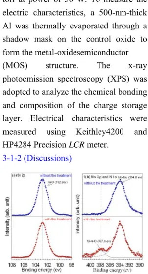
3 FIG. 3. (Color online) (a) Si 2p, (b) Mo 3p, and N 1s core-level spectra of the charge storage layer composed of Mo nanocrystals embedded in SiOx with and without the plasma treatment.
Figure 3 shows the XPS spectra of the charge storage layer with and without the plasma treatment, which was performed
by using a monochromatic Al Kα(1486.6 eV) x-ray. Figure 3(a) shows the XPS Si 2p spectra of the charge storage for the sample with and without the plasma treatment.
For the sample without the treatment in Fig. 3(a), the peak position of XPS Si 2p situated at 102.9 eV indicates that the
surrounding oxide of nanocrystals is SiOx.[1] There is no obvious difference in the peak positions between the samples with and without the treatment. However, it was found that an additional XPS peak (397.8 eV) appears in the Mo 3p and N 1s spectra of the charge storage layer after the plasma treatment, which indicates that the incomplete bonds in SiOx bonded with nitrogen after the plasma treatment, as shown in Fig. 3(b).[2]
FIG. 4. (Color online) C-V curves of the MOS structure with and without the plasma treatment. The inset of the is the simple band diagram of the structure in the flat-band state.
Figures 4(a) and 4(b) show the C-V curves of MOS structure embedded with Mo nanocrystals for the sample with and without the plasma treatment, respectively. At the smaller sweeping voltage of 2 V, there is a negligible memory window in Figs. 4(a) and 4(b) corresponding to the quasineutral state (i.e., no charge is stored in the charge
storage layer under this sweeping range). At the larger sweeping voltages, there are counterclockwise memory hystereses in Fig. 4. The counterclockwise hystereses are due to carrier transport through tunnel oxide between the charge storage layer and the Si substrate. We note that the memory windows of the sample with the plasma treatment are smaller than that without the treatment. For the smaller memory window after the treatment, we speculate the nitrogen passivation in the charge storage layer. It has been suggested that the traps in the oxide around nanocrystals can capture carriers and contribute to the memory window.[3-4] According XPS results, the nitrogen was incorporated into the oxide around the Mo nanocrystals after the treatment. The incorporated nitrogen can passivate the traps in the oxide, which reduces the charge storage centers and leads to the smaller memory window, as indicated in the insets of Fig. 4.
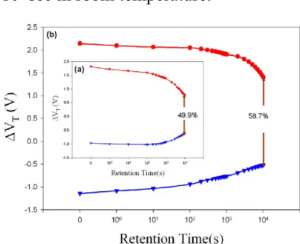
4 FIG. 5. (Color online) The retention behavior of the MOS structures with and without the plasma treatment.
Figure 5 is the comparison of the retention behavior for the samples with and without the plasma treatment. The
retention was measured by a stress voltage of 10 V on Al gate electrode for 5 s. The memory window was obtained by comparing the C-V curves after the programming to the quasineutral state. It can be found in Fig. 5 that, after the 103 s retention time, the decay rate (-66 mV/decade) of the memory window for the sample with the plasma treatment is slower than that without the treatment (-115 mV/decade).
The superior retention of the sample with the treatment can be explained by the nitrogen passivation of the traps in the oxide around Mo nanocrystals. When charges are stored in the nanocrystals, the stored charges can escape with the assistance of traps _traps assist tunneling_ in the surrounding oxide. Because the traps in the oxide were reduced after the plasma treatment, the retention was improved by suppressing the trap assisted tunneling process.
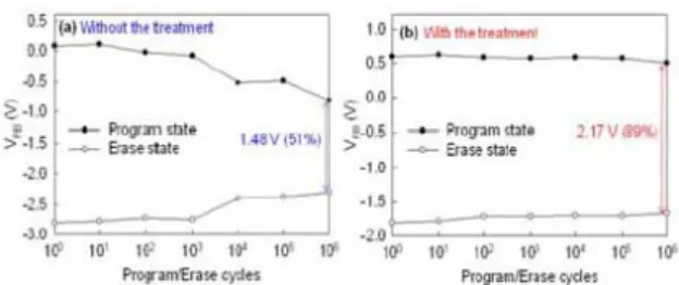
FIG. 6. (Color online) Endurance characteristic of the MOS structures (a) with and (b) without the plasma treatment.
Figures 6(a) and 6(b) presents the endurance characteristics of the samples with and without plasma treatment under the pulse conditions of VG=-15 V for 1
ms, respectively. In Fig. 6(a), the △VFB
programming and erase states) reduced significantly, and the △VFB remained 51% after 106 program/erase cycles. However, the plasma treated sample exhibits robust endurance characteristic (△VFB of 89% after 106 program/erase cycles). It is known that the △ VFB reduction during the endurance test is due to the degradation of the gate oxide.[5]
(3.2 NiSi2/SiNX nanocrystals for
nonvolatile memory devices) 3-2-1 (Experiment)
5
The better endurance characteristics of the sample with the plasma treatment can be attributed to the improvement of quality of the surrounding oxide. During the endurance test, the carriers transport between nanocrystals and the substrate can damage the surrounding oxide, which produces more traps. Because the surrounding oxide was strengthened by the nitrogen incorporation after the treatment, the generation rate of traps reduced, resulting in the better endurance characteristic.
3-1-3 (Conclusion)
The nonvolatile memory characteristics of the Mo nanocrystals were influenced by the ammonia plasma treatment. The
C-V hysteresis reduced to 3.0 V and
retention characteristic improved with decay rate of -66 mV/decade after the plasma treatment due to the nitrogen passivation of the traps in the oxide around the nanocrystals. The incorporation of nitrogen into the charge storage layer through the NH3 plasma treatment can strengthen the endurance characteristic of Mo nanocrystals memory.
This memory-cell structure was fabricated on a 6 inch p-type silicon (100) wafer. After a standard RCA process which removed native oxide and micro-particles, a 4.5-nm-thick tunnel oxide (SiO2) was thermally grown by a dry oxidation process in an atmospheric pressure chemical vapor deposition furnace. Subsequently, three type structure of NiSi2 charge-storage layer was fabricated to compare. About 5~7 nm thick NiSi2 layer was deposited for single-layer (sample A) and double-layer (sample B) nanocrystal storage structure with only Ar 50 sccm. The sample A was also used to be control sample and the two nanocrystal storage layer of sample B was separated by about 3 nm PVD oxide (SiO2). The other structure is also about 5 nm thick nanocrystal storage layer sputtering in the mixture gas of Ar (50sccm) and NH3 (10 sccm) at room temperature to induce the nitride based trap (sample C). After that, about 30nm SiO2 was deposited as control oxide. Nanocrystals can be isolated well and the oxide quality can be improved by rapid thermal anneal in O2 ambiance. Finally, the bottom and top Al electrode was patterned to form the MOS transistors.
3-2-2 (Discussions)
To confirm the formation of nanocrystal, the cross-sectional transmission electron microscope images of the single-layer
(sample A) and double-layer (sample B) structure nanocrystal without reaction gas are shown in Fig. 1(a) and Fig. 1(b), respectively. Obviously, NiSi2 atoms are activated and self-assembled into separate and granular NCs after 700℃ RTA process in O2 ambient. The densities of nanocrystal for sample A and B are estimated to be 2.73×10¹²
cm-2 and 1.43×1012 cm-2, and the
nanocrystal diameters are about 5 nm and 7 nm. The low resolution TEM images are shown in the inset of Fig. 1(a) and Fig. 1(b).
6 Fig. 1 Cross-sectional transmission electron
microscope of (a) single-layer NiSi NCs , and (b) double-layer NiSi NCs embedded in the SiO2. The insert pictures are the low resolution TEM images.
Fig. 2(a) and Fig. 2(b) show the C-V hysteresis of sample A and sample B,
and indicate the memory windows under ±4MV/cm operation are 2.5V and 8.6V, respectively. The memory window of device with double-layer structure is larger than that with single-layer structure due to the fact that more charge storage traps in double-layer structure. Although 0.5V memory window is large enough to identify logic “1” or “0” state, memory device with a larger memory window can stand more electrons loss from the nanocrystal charge storage layer and avoid misidentification.
Fig. 2 Capacitance-voltage (C-V) hysteresis characteristics of memories with (a) single-layer and (b) multi-layer NCs. The memory windows of (a) 2.5 V and (b) 8.6 V can be obtained under about ± 4MV/cm operation, respectively
Figure 3(a) and Figure 3(b) show the threshold voltage shifts (△VT) from flat
band with pulse time for samples A and B. Comparing with sample A, sample B still has an equal memory window even it is operated with a smaller effective electric field.
7 Fig. 3 Electron and hole injection induced threshold voltage shift (△VT) from flat band with pulse time for
devices with (a) single-layer and (b) double-layer nanocrystal structures.
Figure 4(a) and Figure 4(b) show the retention characteristics of the samples A and B, respectively. It can be seen that the decay ratio of sample B is large than that of sample A. Because the coulomb blockade effect induced by the electrons stored in the first layer (the closer layer from Si substrate) can exclude the electrons stored in the second layer (the further layer from Si substrate) from leaking back to the substrate, the stored carrier can be improved from 49.9% (sample A) to 58.7% (sample B) until
104sec in room temperature.
Fig. 4 Retention characteristics of (a) single-layer and (b) double-layer nanocrystal structure at room temperature. The device with double-layer structure has better retention characteristic, 58.7%, at 104 sec than that for single-layer device because of coulomb blockade effect.
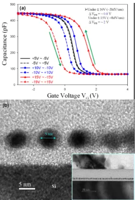
In order to combine the advantages of nonvolatile nanocrystal memory (NVM) and metal/oxide/nitride/oxide/silicon (SONOS) memory, we integrate the nitride traps with NiSi2 nanocrystal by simply reactive sputtering NiSi2 in the mixture gas of argon (Ar) and ammonia (NH3) at room temperature (sample C). The C-V curves of sample C are shown in Fig.5(a), and the memory window under ± 15V operation is about 2V, which is not much different from sample A. The cross-sectional transmission electron microscope images are also shown in Fig. 5(b), and the density and diameter of nanocrystals are estimated to be 1.23×1012cm-2and 5nm, respectively.
8 Fig. 5 (a) C-V hysteresis characteristics and (b) TEM photographs of memory with NiSi2/SiNX compound nanocrystals (CNCs) structure. The memory window under ± 4MV/cm operation is about 2V , and the nanocrystal diameter is identified about 5nm.
As shown in Fig. 6(a), the photoelectron spectra of Ni 2p3/2 of sample C can be separated to two peaks with center at 853.1eV and 855.6eV by fitting with Lorenzian-Gaussian functions. Due to the fact that the bond dissociation energy of Ni-Si (318 kJ·mol-1) is much less than that of N-Si (437.1 kJ·mol-1) , the Ni-Si bond tends to dissociate and react with nitrogen to form the bond of Ni-Si-N and Si-N during sputtering. Hence, the peak with center at 855.6 eV is attributed to the bond Ni-Si-N. As shown in Fig. 6(b), the photoelectron spectra of N 1s of sample C also verified the nanocrystals were composited of N-Si bonding (397.9 eV) and N-Si-Ni
(396.8) again. According to the X-ray photoelectron spectra analyses above, it could be judged that the nanocrystals components of sample C are composed of NiSi2 and SiNX with minor inclusion of NiSiN ternary alloy.
Fig. 6 Peak analyses of XPS spectrum of (a) Ni 2p3/2 and (b)
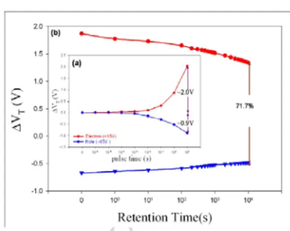
N 1s for sample C with NiSi2/SiNX CNCs structure. The threshold voltage shifts (△VT) from flat band with pulse time for sample C were also shown in Fig. 7(a). The threshold voltage shifts caused by electrons and holes injecting under ± 15V for 10 seconds are about 2.0V and 0.9V, respectively. It is noteworthy that the marked electrons and holes injection happened as the pulse time increases 10-3~10-2 seconds, indicating that the programming and erasing efficiencies of sample C is higher than that of sample A and sample B.
memory device of sample C, the retention characteristic is shown in Fig. 7(b). Since the structure of NiSi2/SiNX CNCs is formed in sample C, the additional potential barrier of nitride can reduce the tunnel probability significantly and the traps contributed by nitride can be used as memory storing centers. Furthermore, the hydrogen atoms which were dissociated from NH3
9
during depositing nanocrystal charge storage layer could passivate the shallow traps of nitride. On account of the deep traps being well below 0.7 eV, the carriers trapped in deep traps were hard to escape during retention test. Hence, in spite of the endurance test has been implemented before the retention test, the decay ratio of memory window for 104 seconds is still better than sample A and B in room temperature. According to the retention results, the proposed device with NiSi2/SiNX CNCs structure indeed exhibits superior reliability than traditional single-layer or even double-layer nanocrystals device.
Fig. 7 (a) Electron and hole injection induced threshold
voltage shift with pulse time, and (b) Retention characteristic after endurance test at room temperature. The retention
characteristic is still better than double-layer structure (sample B) even undergoing endurance test.
3-2-3 (Conclusion)
We have fabricated double-layer (sample B) NCs and NiSi2/SiNX CNCs (sample C) as comparison samples with single-layer (sample A) to investigate the improvement of reliability based MOS memory capacitor. Since the coulomb blockade effect, the nanocrystal device with double-layer structure improves the charge retention performance indeed. This study also incorporates nitrogen into NiSi2 layer by sputtering in NH3 ambience, and the NiSi2/SiNX CNCs can be easily formed after rapid thermal annealing. Comparing with double-layer device, the nitride layer surrounding NiSi nanocrystals can provide the additional tunnel barrier and deep traps to further improve the charge retention characteristic. The combination of nitride based traps with nanocrystal by simple process indeed can provide superior memory reliability for next generation and high-integrated NVM applications.
4、Reference
1. B. Gallas, C. C. Kao, S. Fisson, G. Vuye, J. Rivory, Y. Bernard, and C. Belouet, Appl. Surf. Sci. 185, 317 (2002).
2. Z. H. Lu, S. P. Tay, R. Cao, and P. Pianetta, Appl. Phys. Lett. 67, 2836 (1995).
10
3. C. Busseret, A. Souifi, T. Baron, S. Monfray, N. Buffet, E. Gautier, and M. N. Semeria, Mater. Sci. Eng., C 19, 237 (2002).
4.W. R. Chen, T. C. Chang, J. L. Yeh, S. M. Sze, C. Y. Chang, and U. S.
Chen, Appl. Phys. Lett. 91, 222105 (2007).
5. P. Pavan, R. Bez, P. Olivo, and E. Zanoni, Proc. IEEE 85, 1248 (1997). 5. 計畫成果自評 本計劃今年度延續去年奈米點元件記 憶體特性及可靠度,以解決傳統浮停 夾微縮問題,已經完成了Mo奈米點之 製作及電漿處理對於增加其非揮發性 記憶體之可靠度特性有明顯有效的成 果,且我們成功發展奈米點及高介電 常數材料之整合與多層奈米點之發展 及不同處理方式如超臨界流體處理對 奈米點非揮發性記憶體之影響,相關 成 果 已 整 理 並 逐 步 發 表 於 國 際 期 刊 上。
98 年度專題研究計畫研究成果彙整表
計畫主持人:施敏 計畫編號: 98-2221-E-009-001-計畫名稱:奈米點記憶體元件之製作與物理機制研究(2/2) 量化 成果項目 實際已達成 數(被接受 或已發表) 預期總達成 數(含實際已 達成數) 本計畫實 際貢獻百 分比 單位 備 註 ( 質 化 說 明:如 數 個 計 畫 共 同 成 果、成 果 列 為 該 期 刊 之 封 面 故 事 ... 等) 期刊論文 0 0 100% 研究報告/技術報告 0 0 100% 研討會論文 0 0 100% 篇 論文著作 專書 0 0 100% 申請中件數 0 0 100% 專利 已獲得件數 0 0 100% 件 件數 0 0 100% 件 技術移轉 權利金 0 0 100% 千元 碩士生 0 0 100% 博士生 0 0 100% 博士後研究員 0 0 100% 國內 參與計畫人力 (本國籍) 專任助理 0 0 100% 人次 期刊論文 0 0 100% 研究報告/技術報告 0 0 100% 研討會論文 0 0 100% 篇 論文著作 專書 0 0 100% 章/本 申請中件數 0 0 100% 專利 已獲得件數 0 0 100% 件 件數 0 0 100% 件 技術移轉 權利金 0 0 100% 千元 碩士生 0 0 100% 博士生 0 0 100% 博士後研究員 0 0 100% 國外 參與計畫人力 (外國籍) 專任助理 0 0 100% 人次其他成果