行政院國家科學委員會專題研究計畫 成果報告
半導體奈米結構分散性群體的磁性與磁光特性
研究成果報告(精簡版)
計 畫 類 別 : 個別型 計 畫 編 號 : NSC 100-2112-M-009-009- 執 行 期 間 : 100 年 08 月 01 日至 101 年 07 月 31 日 執 行 單 位 : 國立交通大學電子工程學系及電子研究所 計 畫 主 持 人 : 霍斯科 共 同 主 持 人 : 李建平 計畫參與人員: 博士班研究生-兼任助理人員:蘇聖凱 博士班研究生-兼任助理人員:李依珊 博士班研究生-兼任助理人員:林建宏 公 開 資 訊 : 本計畫可公開查詢中 華 民 國 101 年 10 月 16 日
中 文 摘 要 : 對於半導體元件多功能的日益需求促使了形狀複雜的半導體 奈米物件的發展,其展現出無論在光、電、量子資訊、生醫 影像的發展性。然而,奈米物件本身複雜的變異性(形狀、大 小、組成)造成其物理性質上的極大變異;為了對半導體奈米 物件有更深的了解和更精確的掌握,我們發展出一套一般性 的理論描述半導體奈米物件的物理響應,此理論根據多變異 分布函數可描述不同的物理性質的變異。 在此報告中,我們計算了半導體奈米物件的能階和其對應之 電子電洞波函數,並考慮其形狀、物質參數和分布上的變 異。為了驗證我們的方法,我們對 ZnTe/CdSe 的量子點和 InAs/GaAs 量子環做光譜和磁化率的模擬,其結果和實驗所 得數據相符。 因此我們的這一套理論方法將給予最佳化奈米物件的平均物 理特性很大的幫助。 中文關鍵詞: 磁性,磁光,半導體, 奈米物件, 多變異離散
英 文 摘 要 : Current demand for multiband and multifunctional nano-based semiconductor devices stimulates the development of novel nano-scale semiconductor components (nano-objects). Impressive progress in semiconductor technologies makes it possible to fabricate semiconductor nano-objects with very sophisticated shapes and material compositions: quantum dots, quantum dot molecules, quantum dot posts, and quantum rings, etc. The semiconductor nano-objects demonstrate unique properties those are very promising for modern optics, optoelectronics, quantum information processing, bio and medical imaging, etc. Unfortunately, the inherent dispersion of parameters (shape, size, material composition) leads to fluctuations (some time almost
uncontrollable) of the physical properties of macro-systems combined from the nano-objects. To achieve a proper quantitative description and address the
controllably of macro characteristics of ensembles of the semiconductor nano-objects in this study we have proposed and developed a general theoretical
description of the physical response of dispersive ensembles made from the semiconductor nano-objects of complex geometries and material compositions. The
description is based on the multivariate distribution function, which cumulatively reproduces variations of the objects’ parameters.
In this report we present and discuss our method of multivariate simulation of physical properties of ensembles of semiconductor nano-objects with dispersion in geometry, material parameters, and spatial distributions. Using the mapping method (recently derived by us) we are able to very
efficiently compute energy states and wave functions of electrons and holes confined in the nano-objects within a wide range of sizes, shapes, and
compositions. Thus, using the hybrid multiscale (hierarchical) method we are able to simulate ensembles of nano-objects with multiparametric (multivariate) distributions. To demonstrate our method efficiency we simulated the absorption cross section of ensembles of ZnTe/CdSe core/shell quantum dots and the unusual diamagnetic response (magnetic susceptibility) of ensembles of wobbled InAs/GaAs quantum rings. We have theoretically obtained the actual optical spectra and magnetic susceptibility in a very good agreement with experimental data.
We have proven that our multivariate statistical approach can be useful for optimization of the averaged physical characteristics of the dispersive ensembles of nano-objects.
英文關鍵詞: magnetism, magneto-optics, semiconductor, nano-objects, multivariate dispersion
1
Magnetic and magneto-optical properties of dispersive ensembles of semiconductor nano-objects
Contents
1. Introduction (Purpose and Brief Literature Review) 2
2. General description of the dispersive ensembles of semiconductor nano-objects.
Multivariate approach 4
3. Spectral characteristics of dispersive ensembles of semiconductor core-shell
quantum dots 5
4. Impact of size and shape dispersion on the averaged magnetic response of ensembles of
semiconductor quantum rings 8
2
Magnetic and magneto-optical properties of dispersive ensembles of semiconductor nano-objects
1. Introduction (Purpose and Brief Literature Review)
Advances in modern semiconductor technologies make it possible to produce semiconductor nano-objects within a wide range of geometrical shapes and material parameters (quantum dots, nano-rings, quantum dot molecules, quantum dot posts, nano-rods, etc.), investigate their properties in details, and use them for various applications (see for instance [1-3] and references therein). Those nano-objects are thought to be very promising candidates for practical use in optics [4], quantum information processing [5], nano-biology, nano-medicine [6]. Nano-structured semiconductor meta-materials [7-9] also offer a very promising direction of the future development of novel semiconductor device components and subsystems. All unique and useful properties of the systems assembled form nano-objects are derived from properties of the constituent elements. Therefore, incorporating controllable and tunable nano-objects into nano-structured systems and meta-materials leads to tunable (on the quantum level) properties of them. It is well known, that to perform large-scale quantum information processing systems assembled form many all uniform and regular nano-sized elements are required. The same requirements are of the paramount impotence in nano-optics and nano-medicine. But, the inherent dispersion of the semiconductor objects' geometrical parameters (shapes, sizes, material compositions) leads to fluctuations (some time almost uncontrollable) in the demanded in practice parameters and properties of macro-systems combined from the nano-objects. For instance in optics, the dispersion in the nano-objects parameters leads to inhomogeneous broadening in optical spectra, which can drastically decrease applicability of the integrated optical systems. In quantum information processing the fluctuations result in non-controllable decoherence in the quantum bits' entanglement.
The knowledge of the physical properties of semiconductor nano-sized objects with respect to their transport, magnetic and optical properties has increased considerably recently. However, we should conclude, that the important issue of impacts of the parameters' dispersions in ensembles of semiconductor nano-objects on the ensembles' collective properties was much less emphasized, realized, and investigated so far. Unfortunately, among all consequences of the dispersion in the physical characteristics of ensembles of nano objects only optical properties called some attention in the theory. For instance, simple descriptions of the inhomogeneous broadening in the optical absorption spectra of ensembles of semiconductor quantum dots with primitive spherical or cubic shapes are known in literature (see for instance [10,11] and references therein). For semiconductor nano-objects with primitive shapes the broadening was modeled only as a result of the primitive dispersion of the sizes (volumes): volume's variations for cubes and radius' variations for spheres. Such basic approximations for geometries allow us to investigate the broadening using simple analytical expressions, or simple numerical simulations. This "retardation" in the theoretical studies of the collective properties of dispersive ensembles of nano-objects originates from a demand of massive and severe computational tasks to be performed. Most of the present theoretical studies in this domain still focus upon a primitive description of the objects and ensembles. The corresponding knowledge about possible methods and means to insure predictable and controllable magneto and magneto-optical parameters of random and dispersive ensembles of semiconductor nano-objects is particularly weak. It is the central aim of this project to fill in the gap for this emergent research field.
The general approach to the realistic theoretical description of dispersive ensembles of semiconductor nano-objects with complex material parameters and geometrical shapes is to consider a multivariate (multidimensional) distribution function [12,13] including dispersions of all appropriate physical parameters. This requires computational methods those can optimize extensive simulations of the physical properties of semiconductor nano-objects within wide ranges of variations of their parameters. We recently developed two efficient computational methods. The fist one is the hybrid multiscale (hierarchical) method which allows us to simulate and analyze electrical, magnetic, and magneto-optical characteristics of complex semiconductor nano-structures
3
[14-17]. The second is the mapping method with which we are able in a very efficient computational manner obtain the energy states and wave functions of the electrons and holes confined in nano-objects with very sophisticated shapes and material content [18,19]. A proper combination of those two methods makes it possible to simulate and study physical properties of dispersive ensembles of semiconductor nano-objects within a wide range of changes in geometry, material parameters, and spatial distributions.
The purpose of this one-year theoretical project was to address most important problems in this emergent research field and to develop a combined computational procedure of simulations of the static magnetic and electro-dynamic characteristics of three-dimensional semiconductor nano-objects of geometries and material content changes within a wide range. This includes an implementation of the mapping method to formulate statistical description of the dynamic electric polarizability and magnetic susceptibility for single and few quasi-particle (electrons, holes, and excitons) confined in semiconductor nano-objects (such as quantum dots and nano-rings).
[1] Semiconductor nanostructures, Eds. D. Bimberg, Springer, Berlin (2008). [2] G. Konstantatos and E. H. Sargent, Nature Nanotechnonogy 5, 391 (2010). [3] B.C. Lee, O. Voskoboynikov, and C.P. Lee, Physica E 24, 87 (2004).
[4] Optics of quantum dots, Eds. G. W. Bryant, G. S. Solomon, Artech House, MA (2005).
[5] O. Voskoboynikov, Nonvolatile Quantum Memory, Chapter in the collective monograph “NONVOLATILE MEMORIES Materials, Devices and Applications”, Edited by Tseung-Yuen Tseng and Simon M. Sze, Chapter 15, Vol. 2, pp. 377-400, American Scientific Publishers, CA, USA, Jan. 2012.
[6] Biomedical Nanostructures, Eds. K. E. Gonsalves et al., John Wiley & Sons, Inc., NJ, 2008. [7] V. G. Veselago, Sov. Phys. Usp. 10, 509 (1968).
[8] W. J. Padilla, D. N. Basov, and D. R. Smith, Mater. Today 9, 28 (2006).
[9] Electromagnetics of Metamaterials, A. K. Sarychev and V. M. Shalaev, World scientific, 2007. [10] V. I. Belyavskiy and S. V. Shevtsov, Semiconductors, 36, 821, 2002.
[11] D. L. Ferreira and J. L. A. Alves, Nanotechnology 15, 975, 2004.
[12] Methods of Multivariate Analysis, A. C. Rencher, 2nd ed., Wiley-Interscience, New York, 2002.
[13] Applied Multivariate Statistical Analysis, W. Härdle and L. Simar, 2nd ed.,Springer, Berlin, 2002.
[14] O. Voskoboynikov, C.M.J. Wijers, J.J. Liu and C.P. Lee, Phys. Rev. B 71, 245332 (2005). [15] O. Voskoboynikov, G. Dyankov and C.M.J. Wijers, Microelectronics Journal 36, 564 (2005). [16] O. Voskoboynikov, C.M.J. Wijers, and C.P. Lee, Europhys. Lett. 70, 656 (2005).
[17] C. M. J. Wijers, J.-H Chu, L. J. Liu, O. Voskoboynikov, Phys. Rev. B 74, 035323 (2006). [18] L. M. Thu and O. Voskoboynikov, Phys. Rev. B 80, 15542 (2009).
4
2. General description of the dispersive ensembles of semiconductor nano-objects. Multivariate approach.
Up to now most of simulations of the statistical physical characteristics of dispersive ensembles of semiconductor nano-objects were devoted to the inhomogeneous broadening in optics of ensembles of semiconductor quantum dots. The simulations were performed for simple spherical or cubic shapes of the dots and the broadening was attributed to the dot-size (volume) primitive univariate (single-parameter, for instance the dot radius) dispersion. This approach allows for simple analytical expressions and non-extensive numerical simulations. However, it is obviously not applicable to most of the nano-objects. The general approach to the realistic theoretical description of dispersive ensembles of semiconductor nano-objects with complex material parameters and geometrical shapes is to consider a multivariate (multidimensional) distribution function including dispersions of all appropriate physical parameters (subsets of parameters of interest). This requires computational methods those can optimize extensive simulations of the physical properties of semiconductor nano-objects within wide ranges of variations of their parameters.
The spatial, geometrical, material parameters’ dispersions in ensembles of nano-objects can be described by a multivariate (multidimensional) joint distribution function P({x1, x2, . . . , xn}). The objects' spatial distribution (the actual positions within the ensembles) can be presented by a sub-set of discrete parameters {i} (objects' coordinates). The structural (geometrical and material) characteristics of the dots are presented by a sub-set of appropriate continuous parameters {j}. Then function P({i};{j}) presents the dispersions of all appropriate parameters {xk}. This gives the number of nano-objects dNi with the values of {i} and {j} inside the domain (i ;{i,i + di}) as
j j j i d P dN , .The cumulative expectation (meaningful average) of a physical quantity Q({i},{j}) characterizing the ensemble then is written as
j j j j i j i i d Q P Q };{ };{Most of the ensembles can be characterized satisfactorily when only a subset of the parameters in {xk} is of any interest. Therefore, we can consider the conditional distributions for
subsets of the parameters of interest: {xk }C ⊆ {xk}. Accordingly, when it is possible to neglect
dispersions of the other (“nuisance”) parameters we can define the appropriate conditional expectation as
C j j j j i j i C i C P Q d Q };{ };{ ) (In our consideration we assume that the parameters in a typical nano-objects’ ensemble follow the non-correlated normal distribution which is presented by
k k k P x x P5
Now to simulate the spatial disorder in ensembles of nano-objects we create a compact cluster consisting of N cubic cells within a certain volume. Nd cells of the cluster are occupied by a single nano-object in each (Nd < N). We randomly locate the occupied cells within the cluster and calculate the physical quantity of our interest Q. Then we randomly relocate occupied cells again and again. Notice that the dots density (Nd /N) remains the same for all tries. We can repeat the procedure many times and obtain the conditional average (when a sub-set {j} is fixed):
,
i i i C P Q Q where the discrete uniform distribution is presented by the number of dot relocations Z as P{i} = 1/Z.
The structural dispersion rises from variations of the individual nano-objecs' parameters when we stick with a certain set of the dots' locations in the ensemble (cluster). This multi-dimensional distribution is presented by
j , j G j P P
where the standard normal distribution for each parameter j is written as
0 , A G PGA is the normalization coefficient, 0 is a mean value, is the standard deviation of the
parameter, and G() is the Gaussian function.
C j j j j j G C j C Q P d Q 3. Spectral characteristics of dispersive ensembles of semiconductor core-shell quantum dots. One of the most exciting meeting points of the semiconductor nanophysics and nano- biology is the use of semiconductor quantum dots for "in vivo" biomedical imaging. The robust identification of targeting biomolecules conjugated with QDs requires for a very high recognition accuracy of the photoluminescence spectral characteristics of QDs' ensembles. At the same time the inherent property of semiconductor QDs is their geometrical and material parameters’ dispersions. This generates disorder in the quantum confinement of the dots and leads to non-homogenous broadening in the absorption and emission spectral lines of the dots. The broadening obviously obscures the biomedical imaging. In addition the broadening can be enhanced by the random spatial locations of the dots in bio-tissues.
We use our hybrid discrete/continuous model (L. M. Thu and O. Voskoboynikov, Phys. Rev. B 80, 15542, 2009) to describe the optical response of the ensembles (systems) of the dots by means of polarizabilities of effective discrete dipoles dl embedded into a continuous transparent dielectric medium with the dielectric constant m . We can assume that a dipole dl is located in the center of the lth cell of the ensemble (cluster) like it was described above. In the linear discrete dipole approximation (DDA) the dipole is characterized by the excess bare polarizability tensor Bl() of a single QD, which at the near of optical resonance transition can be written as:
), ( ) ( Sl lD l B α α α
6
where is the incident light frequency, S() is the static part and D() is the dynamic part of the polarizability.
The light absorption cross section defined as the following:
}, 3 2 Im 4 * 3 * * 1 2 0 abs l l N l l Dl l m k k C d d d d d E
where
1
1 Bl lS Dl α t α is the dressed polarizability, tS is the full electromagnetic self-interaction tensor for the QDs, k = /c and E0 stand for the wave vector and electric field amplitude of the incident light, c is the light
speed in the vacuum.
The dipole strength dl should be found from the following system of equations
, ' '
l Xi l lld E T where
, ˆ 6 , ) 1 ( 3 0 3 ' ' 1 ' ' I t t F t α T c i m S l l ll ll l Bl ll ll and Fll' is the vacuum intercellular (inter-dipole) transfer tensor (the dyadic Green’s function in the DDA).
The dynamic part is described by means of Kramers/Heisenberg type of polarizabilities. Ignoring quantum nonlocal effects the dynamic part of the tensor of the bare embedded polarizability (which has been derived by us) can be written in terms of the electro-hole overlap integrals and transition energies. To find the static part of the polarizability tensor we implemented an appropriate boundary-value problem for a local electrostatic potential in a complex three-dimensional cubic domain of the host material including one nano-object.
Considering in the vicinity of the ground state excitonic resonant optical transition of the dot (which generates a peak in an optical spectrum), we can write the dynamic part of the polarizability as the following [10]:
i E f E e ex ex T eh eh ex D r r α * 2 ) (
where fex = ex(r)2 is the squared electron-hole overlap integral, ex(r) and Eex stand for excitonic wave function and energy, represents the homogeneous (temperature) broadening of the peak, and reh is the semiconductor bulk interband optical matrix element.
For the dynamic part of the polarizability we computed the transition energies and wave functions of electrons and holes confined in the semiconductor nano-object. Our general method allows us to simulate the nano-objects of arbitrary shapes. The electron states are described by means of the effective one-band Hamiltonian with the energy and position dependent effective mass. The valence-band hole states in semiconductor nano-objects (preferably III-V semiconductor compounds) we describe with multiband (4x4) k·p Hamiltonian that allowed for valence subband mixing. The electrostatic characteristics, energy states and wave functions of electrons and holes confined in the quantum dot molecules are obtained numerically form solutions of the Schrödinger equation with the appropriate effective Hamiltonians (we use realistic semiconductor material parameters for strained semiconductor heterostructures, with corrected to the strain condition band parameters, etc.) by the nonlinear iterative method using COMSOL multiphysics package.
We applied the approach described above to ensembles of type-II ZnTe/CdSe core/shell QDs in the toluene solution (the ensembles those were experimentally investigated, see Fig. 1)
7
Figure 1. (a) ZnTe/CdSe core/shell QDs.
(b) Potential profiles for electrons and holes.
We first consider the spatial disorder and choose h =1.2 nm for all dots within the cluster. According to our simulation experience, for several tries of the dot random relocations, the averaged absorption cross section barely differs from an individual try's result. The homogeneous broadening (variations of ) does not affect this finding. When we repeated the procedure choosing different h we found the same stable behaviour of the averaged absorption cross section. Therefore, we conclude that the spatial disorder has a weak influence on the broadening. This suggests a weak interaction between the semiconductor dot dipoles in the cluster (in contrast to the clusters of metallic nano-particles).
We model the structural dispersion within the dot ensembles using our numerical solutions for few different values of h. Then we fit the results of those simulations to the excitonic energy Eex and the squared overlap fex as functions of the shell thickness h using the following guesses: Eex(h) = 1. 923h-0.27 eV and fex(h) = -0.001+0.98 (h+1.3)-1 - 0.42(h+1.3)-2 (h is presented in nm).
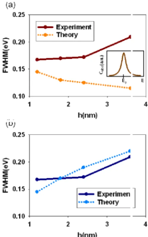
Figure 2. FWHM for (a) uniform (inset: Ep
marks the peak position) and (b) non-uniform
Figure 2a shows results of our simulations of the full width at half maximum (FWHM) of the excitonic spectral peaks at the room temperature (T = /kB = 300 K, kB is the Boltzmann constant)
8
when the relative standard deviation of the shell thickness (RSDST) h/h0 is chosen to be of 0.15
(uniform) for all ensembles. We should notice that at the present time an actual value for the RSDST cannot be clearly restored from experimental data. Therefore, in this study we can only speculate that the RSDST can vary within a range of 0.1 ÷ 0.3. Clearly (see Figure 2a), the proposition of the uniform RSDST cannot explain the general tendency of the experimental data. To comprehend the experimental results we should impose an increase of h/h0 (when the shell
thickness increases) as the following: h/h0 = 0.1 for h0 = 1.2 nm, h/h0 = 0.13 for h0 = 1.8 nm,
h/h0 = 0.16 for h0 = 2.4 nm, and h/h0 = 0.20 for h0 = 3.6 nm. Figure 2b shows the FWHM for the
ensembles with the RSDST corrected as it was proposed above. The tendency demonstrates a very good agreement with the experiment.
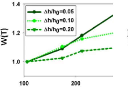
Figure 3. Normalized FWHM for different
relative standard deviations and h0=3.6 nm .
In addition, in Figure 3 we demonstrate the accumulated impacts of the structural dispersion and temperature on the FWHM of excitonic peaks. We present a normalized value: W(T) = FWHM(T)/FWHM(T=100 K). Clearly, the homogeneous broadening plays a minor role when the structural dispersion is large. At the same time, at higher temperatures and moderated structural dispersions the temperature influence becomes significant.
4. Impact of size and shape dispersion on the averaged magnetic response of ensembles of semiconductor quantum rings
Using the mapping method we address the issue of the statistical description of the static magnetic response of dispersive ensembles of three-dimensional InxGa1−xAs/GaAs self-assembled quantum rings (SAQRs) - nano-objects with a very complex geometry. According to recent experimental results the SAQRs demonstrate controllable flexibility of geometrical and material characteristics. The most intriguing property of the SAQRs, that has attracted much attention, is their three-dimensional nonsimply connected topology. The property enables topological quantum effects for charged particles confined in the SAQRs (similar to the Aharonov-Bohm effect). This results in a very specific static magnetic response of the rings: when the external magnetic field is applied in the SAQR growth direction, the nonsimply connected topology enables the Aharonov-Bohm oscillations of the ring’s magnetization and generates a positive peak in the differential magnetic susceptibility. effect has to be addressed to the crossing between the two lowest-energy states of the electron confined in the ring. The effect was recently experimentally confirmed at low temperatures for InxGa1−xAs/GaAs self-assembled capped wobbled quantum rings. It was shown that for one-electron rings the wobbling asymmetry can have a strong effect on the magnitude of the first magnetization oscillation and susceptibility peak as well as their positions. However, the actual experimental magnitude of the peak’s height and its temperature dependence remain in a contradiction to the conventional expectations. Unlike the conventional simulations, the experimental peak demonstrates a negligible temperature effect.
Using our mapping method we analyze conditional and simultaneous impacts of the multivariate dispersion of different geometrical properties (parameters) of the SAQRs on the first
9
oscillation in the magnetic response of the rings’ ensembles. We show that our approach makes it possible to verify which specific parameter can play a crucial role in the unusual magnetic response. In addition, we address the issue of the temperature stabilization of the static magnetic response of the dispersive ensemble of SAQRs. In our method we assume (this is a very standard condition)
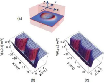
Figure 4. (a) Capped wobbled InxGa1−xAs/GaAs
self-assembled quantum ring. Two projections of the electronic confinement potential on (b) (x,0,z) and(c) (0,y,z) planes (Rr = 11.5 nm,
ξ = 0.2).
that the object was grown at a flat substrate parallel to (x,y) plane (Fig. 3). The height of the object in z-direction (the system growth direction) is presented by a function h(x,y). Using analysis of the experimental structural and composition information obtained from AFM (atomic force microscopy) and X-STM (cross-sectional scanning tunneling microscopy) measurement the function h(x,y) can be readily discovered and even analytically approximated for most of the objects.
,
. ; 0 ) , ( , , 1 ) , ( ; 0 , , , ) , ( 1 ) , ( 2 2 2 2 2 2 2 2 2 2 0 2 2 2 2 2 0 0 2 2 2 2 0 r M r r M R y x y x r y x r y x r h y x y x h h y x h y x r y x r y x r R R h y x y x h h y x h where Rr is the ring’s rim radius; h0,hr , and h∞ correspondingly stand for the height at the center of the rings, at the rim, and far outside of the ring; γ0 and γ∞, respectively, determine the inside and outside slopes near the ring’s rim. The wobbling parameter ξ defines the anisotropy (asymmetry) of the ring height on the x-y plane.
The three-dimensional confinement potential V(x,y,z) (Fig. 4) for electrons can be found from the composition dependent band offset.
a y x h z a z E z y x Ve C 1 tanh 1 tanh ( , ) 4 1 1 ) , , (
10
where EC is the electronic band offset in the system. The mapped confinement potentials we use to define the mapping functions
, , , 1 ) , , ( C e E z y x V z y x M
This function accumulates all experimental information about geometrical shapes and compositions of the rings and it allows us to present the position-dependent effective band parameters of electrons (holes) (effective masses, band gaps, etc.) and dielectric constant of the system as well. The energy of the electronic eigenstates Ei and corresponding envelop wave functions of electrons now can be found like it was described in Section 3 (see Fig. 5).
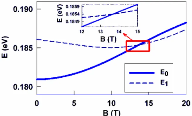
Figure 5. Two lowest electron energy levels for the ring with Rr = 11.5 nm and ξ = 0.2. Inset: crossing region.
At low temperatures the magnetization
i B i i T k B E B B E Z B F T B M( , ) 1 ( )exp ( ) and susceptibility B T B M T B ( , ) ) , ( of a ring are defined by the magnetic-field dependencies of the lowest-energy states. It is known that the first oscillation of the magnetization and correspondingly the first positive peak of the susceptibility appear at the crossing of the ground E0 and first excited E1 electron energy levels (manifesting the Aharonov-Bohm effect). Therefore, for clarity in this study we concentrate on the first oscillation of the magnetic parameters of the rings. At the neighborhood of the crossing point Bc we can suggest that (see also as an illustration Fig.5)
C B B B (B) E C ) (B - B ) + C (B E (B) E , C C , 1 0 1 , 0 1 , 0 0 1 0
Actual values of the electronic energies near the first crossing, amplitudes of the magnetization oscillation, and susceptibility peak [defined by Bc and C0(1)] strongly depend on the actual
11
geometrical and material parameters of the rings such as effective radii, heights, material content, strain, etc. Therefore, in general, within our approach we can characterize them by a set of parameters {xi} ⇒ {Rr , ξ, h0, hr, . . . ,m in(out) . . .}. From an experiment one actually obtains values
of the magnetic characteristics averaged over an ensemble of the rings with dispersions of certain selected parameters combined into the conditional set {xi}C.
We have to keep the parameters’ variations within certain bars to guarantee the appearance of the crossing and oscillations. Therefore, in this paper we confine ourselves to a bivariate (two-dimensional) distribution for the variations when only the parameters Rr and ξ vary (the conditional subset {Rr ,ξ }C). For this subset the meaningful averages for the magnetization and differential magnetic susceptibility characterizing the ensemble can be written as
and
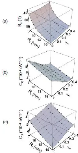
The energy states are obtained numerically from solutions of the full three-dimensional eigenvalue problem. Values of BC({Rr ,ξ }C) and C0(1) ({Rr ,ξ }C) are reproduced from the calculation results for the corresponding sets {Rr ,ξ }C (see Fig. 6).
Figure 6. Dependencies of the electronic energy
characteristics on the rim radius Rr and wobbling parameter ξ: (a) crossing point Bc, (b) coefficient C0, and (c) coefficient C1. Dots,
simulation data; surface plots, appropriate fitting functions.
The results of those simulations we fit to the two-dimensional functions BC({Rr ,ξ }C) and C0(1) ({Rr ,ξ }C)Bc({Rr ,ξ }C) using the following guess:
d dR R P R T B M T B M r r r r R ) , ( ) , , , ( = ) , (
. ) , ( ) , , , ( = ) , ( d dR R P R T B T B r r r r R
12
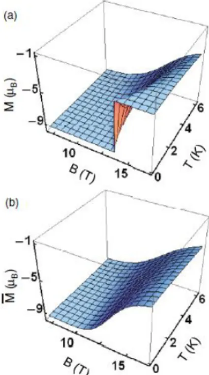
Figure 7. Dependence of the magnetization M on
the temperature and magnetic field for (a) individual ring (Rr = 11.5 nm, ξ = 0.2) and (b) rings’ ensemble ( Rr = 11.5 nm, ξ = 0.2,
dispersion 5%).
Xk(Rr ,ξ ) = ak + bkξ + ckξ 2 + dkξ 3 + ekRβk
where k = 0,1,c and Xk(Rr ,ξ ) = (C0,C1,Bc). According to our experience, the best fit can be achieved with the fitting parameters given in Table I (in appropriate International System units).
Using Bc(Rr ,ξ ) and C0(1)(Rr ,ξ ) from the fit we are now able to simulate the conditional meaningful averages for the magnetization and differential magnetic susceptibility characterizing dispersive ensembles of one-electron InxGa1−xAs/GaAs SAQRs and compare that with magnetic properties of an individual ring and the actual experimental data. Figures 7 and 8 show results of our simulation for the temperature-dependent magnetization and differential magnetic susceptibility of an individual InxGa1−xAs/GaAs ring with Rr = 11.5 nm and ξ = 0.2 and the same values averaged within the ensembles of the rings with the mean values Rr = 11.5 nm, ξ = 0.2 when the geometrical parameter dispersions are taken to be 5% both for Rr and ξ . Clearly, for the individual SAQR at very low temperatures the magnetization rapidly oscillates [Fig. 7(a)] and the differential magnetic susceptibility demonstrates a very sharp symmetrical positive peak [Fig. 8(a)] near the crossing point.
Figure 8. Dependence of the differential magnetic
susceptibility χ on the temperature and magnetic field for (a) individual ring (Rr = 11.5 nm, ξ = 0.2) and (b) ring ensemble
The oscillation and peak become wider and disappear very rapidly when the temperature increases. This is in contrast to the experimental data, where the relatively wide peak reveals itself even when the temperature increases. The temperature stable magnetization oscillation and temperature stable
13
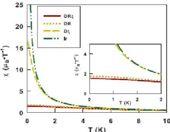
wide peak (inhomogeneous broadening) of the differential magnetic susceptibility indeed can be explained only by the geometry dispersion in the ring ensembles even if the dispersions are taken to be only 5%. To demonstrate that, in Figs. 7(b) and 8(b) we present the simulation results for the conditional averages of the magnetization and magnetic susceptibility of the ensemble of the rings with Rr = 11.5 nm and ξ = 0.2. Our conditional multivariate approach allows us to clarify which parameter’s fluctuations are most relevant to the temperature stabilization of the differential magnetic susceptibility of the chosen model of the geometry of the wobbled InxGa1−xAs/GaAs SAQRs. In Fig. 9 we show the temperature dependence of the conditional averages of the height of the positive peak of the magnetic susceptibility (at the crossing point Bc) when two parameters (Rr and ξ) are varying separately and simultaneously while the mean values Rr = 11.5 nm and ξ = 0.2. Clearly, within the low-temperature range, in this ensemble the broadening due to the ring’s rim radius variation (the crossing point deviations) plays a crucial role in the overall inhomogeneous broadening and temperature stability of the positive peak of the differential magnetic susceptibility.
Figure 9. Temperature dependence of the height of
the peak of the magnetic susceptibility (inset: small temperature region). DRξ, DR, Dξ , and Ir correspondingly stand for conditional
bivariate dispersion of Rr and ξ (mean values: average Rr = 11.5 nm, ξ = 0.2, dispersion
5%), univariate dispersion of Rr (mean value: Rr = 11.5 nm, dispersion 5%, ξ = 0.2), univariate dispersion of ξ (mean values : Rr = 11.5 nm, ξ = 0.2, dispersion
5%), and individual ring with Rr = 11.5 nm, ξ = 0.2.
In Fig. 10 we present a wider view of the Rr and ξ dispersions’ impact on the temperature stabilization of the magnetic response of dispersive ensembles of the ring for conditional averages Rr = 11.5 nm and ξ = 0.2. For both δR =Rr/Rr and δξ = ξ/ξ the dispersion interval expansion obviously stabilizes the temperature characteristics of the response.
Figure 10. Dependence of the height-to-height ratio
for the averaged peaks of the magnetic susceptibility at 1.2 K ( χ1.2)
14
In general, for a large dispersion the stabilization is achieved at small values of the peak magnitudes. At the same time an appropriate δξ can make the ensemble magnetic characteristics more tolerant to the deviations of Rr (see Fig. 10). The optimization of the ensemble characteristics by a proper control of Rr and ξ gives us an opportunity to design an ensemble of the rings with a large enough and temperature stable peak in the collective magnetic response.
We should note that, using our multivariate approach, we are able to draw a conditional “statistical portrait” of the magnetic response of the ensembles. This makes it possible to clarify the important question of which geometrical parameters’ dispersions are crucial for the formation and properties of the physical response of ensembles of self-assembled semiconductor quantum rings. Therefore, our simulation results for the InxGa1−xAs/GaAs SAQRs within a bivariate geometrical dispersion model suggest directions to the optimization of the unusual static magnetic response for dispersive ensembles of the rings. We suggest that the optimization of the rings’ characteristics can help to design ensembles of the rings with large enough and temperature stable unusual collective magnetic response. This can be potentially useful for further fabrication of composite systems (metamaterials) with principally new magnetic properties.
15
Publication list (August 2011-July 2012) Referred publications:
1. L. M. Thu and O. Voskoboynikov, “Electromagnetic Response of Three-Dimensional Arrays of Quantum Dot Molecules”, AIP Conf. Proc., Vol. 1400, pp. 405-410, Dec. 2011.
2. Yu L. Hsueh, Le M. Thu, O. Voskoboynikov, “Simulation of Spectral Characteristics of Dispersive Ensembles of Semiconductor Quantum Dots”, International Journal of Advances and Trends in Engineering Materials and their Application, Vol. 1, No. 1, pp. 31-39, Jan. 2012. 3. O. Voskoboynikov, “Nonvolatile Quantum Memory”, Chapter in the collective monograph
“NONVOLATILE MEMORIES Materials, Devices and Applications”, Edited by Tseung-Yuen Tseng and Simon M. Sze, Chapter 15, Vol. 2, pp. 377-400, American Scientific Publishers, CA, USA, Jan. 2012, ISBN: 1-58883-250-3.
4. L. M. Thu, W. T. Chiu, and O. Voskoboynikov, “Effect of size and shape dispersion on the averaged magnetic response of ensembles of semiconductor quantum rings”, Phys. Rev. B, vol. 85, no. 20, pp. 205419-1-9, May. 2012.
Conference abstracts:
1. O. Voskoboynikov, "Why the "negative”-diamagnetism of ensembles of semiconductor nano-rings is so temperature stable?", Nanophotonics and nanoelectronics: materials and physics II, Taiwan-Russian Joint Symposium 2010, NCHU, Taiwan, Oct. 2010.
2. O. Voskoboynikov, L. M. Thu, W. T. Chiu, “Geometrical asymmetry and suppression of diamagnetic shifts of excitonic energies in self-assembled quantum rings”, Nanomaterials and Nanotechnology, Peer Reviewed Book, Abstracts of ICNANO-2011, p. 45, VBRI PRESS, India, Delhi, Dec. 2011.
3. O. Voskoboynikov, L. M. Thu, W. T. Chiu, “Excitonic wave function collapse in asymmetrically wobbled self-assembled quantum rings”, 10th International Conference on Excitonic Processes in Condensed Matter, Nanostructures and Molecular Materials, Abstract Book, P134, Groningen, The Netherlands, July 2012.
國科會補助計畫衍生研發成果推廣資料表
日期:2012/10/16國科會補助計畫
計畫名稱: 半導體奈米結構分散性群體的磁性與磁光特性 計畫主持人: 霍斯科 計畫編號: 100-2112-M-009-009- 學門領域: 半導體物理-理論無研發成果推廣資料
100 年度專題研究計畫研究成果彙整表
計畫主持人:霍斯科 計畫編號: 100-2112-M-009-009-計畫名稱:半導體奈米結構分散性群體的磁性與磁光特性 量化 成果項目 實際已達成 數(被接受 或已發表) 預期總達成 數(含實際已 達成數) 本計畫實 際貢獻百 分比 單位 備 註 ( 質 化 說 明:如 數 個 計 畫 共 同 成 果、成 果 列 為 該 期 刊 之 封 面 故 事 ... 等) 期刊論文 0 0 100% 研究報告/技術報告 0 0 100% 研討會論文 0 0 100% 篇 論文著作 專書 0 0 100% 申請中件數 0 0 100% 專利 已獲得件數 0 0 100% 件 件數 0 0 100% 件 技術移轉 權利金 0 0 100% 千元 碩士生 0 0 100% 博士生 0 0 100% 博士後研究員 0 0 100% 國內 參與計畫人力 (本國籍) 專任助理 0 0 100% 人次 期刊論文 80 80 100% 研究報告/技術報告 100 100 100% 研討會論文 100 100 100% 篇 論文著作 專書 7 7 100% 章/本 申請中件數 0 0 100% 專利 已獲得件數 0 0 100% 件 件數 0 0 100% 件 技術移轉 權利金 0 0 100% 千元 碩士生 0 0 100% 博士生 3 3 100% 博士後研究員 0 0 100% 國外 參與計畫人力 (外國籍) 專任助理 0 0 100% 人次其他成果
(
無法以量化表達之成 果如辦理學術活動、獲 得獎項、重要國際合 作、研究成果國際影響 力及其他協助產業技 術發展之具體效益事 項等,請以文字敘述填 列。)Cooperation with RAS (Russia Academy Science), Twente University (the Netherlands) 成果項目 量化 名稱或內容性質簡述 測驗工具(含質性與量性) 0 課程/模組 0 電腦及網路系統或工具 0 教材 0 舉辦之活動/競賽 0 研討會/工作坊 0 電子報、網站 0 科 教 處 計 畫 加 填 項 目 計畫成果推廣之參與(閱聽)人數 0