1997 IEEE International Symposium on Circuits and Systems, June 9-12,, 1997, Hong Kong
Analog Maximum, Median and Minimum Circuit
Shen-Iuan Liu, Poki Chen, Chin-Yang Chen and Jenn-Gwo Hwu Department of Electrical Engineering
National Taiwan University
Taipei, Taiwan, R.O..C. China
Abstract
In this paper, we present a new analog maximum, median and minimum circuit with a new preamplifier. This circuit can be used for sorting multiple-input analog signals. The median circuit has been implemented in a 0.8pm single-poly double-metal (SPDM) CMOS process. The measured output error of this median circuit is less than 2.5mV. Its frequency response can be up to 1MHz. The maximum and minimum circuit are also verified by simulations. The experimental and simulation results confirm with the theoretical analysis.
I. Introduction
Median filters play an important role in many applications, such as digital signal
processing and image processing [ 1-71.
Median circuit is the core circuit for a median
filter. Maximum and Minimum circuits are also the important building blocks for fuzzy applications such as process control, robotics
and expert systems [8- 1 01. Conventionally,
the median, maximum, minimum circuits can be implemented in either digital or analog forms [l-71. For the median circuits, the most
common analog approach is based on a
feedback configuration [ 5 ] . However, there is
a poor transfer characteristic with important 'corner' errors. One way to decrease the corner errors is to use a limiting amplifier with a reduced linear range in stead of simple differential pairs. But the errors is still
significant. An improved approach is to place
an additional gain stage in the front of the
differential pairs [ 5 ] . This method requires an amplifier for each input and becomes fairly complex for multiple- input circuits. In this
paper, we proposed a new median, maximum
and minimum circuit with a new preamplifier which can be used for multiple inputs and this circuit is quiet compact.
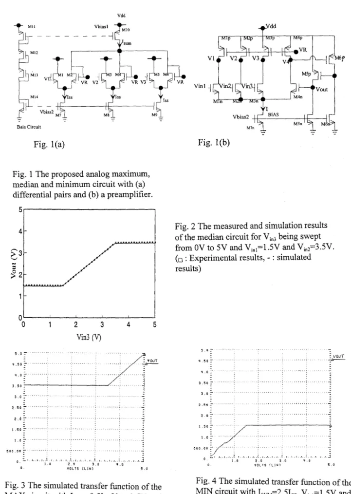
11. Circuit Description
The core circuit of this proposed analog maximum, median, and minimum circuit, which consists of three conventional
differential pairs and a current source Ism, is
shown in Fig. l(a). The operation principle of
this circuit is explained as follows: Assume
that these three differential pairs are matched.
Let the voltages Vk (k=1,2 and 3 ) be input
voltages and V, be the output voltage (in fact, the voltages V, and V, are not the true input voltages and the output voltage). If a maximuim (MAX) operation is required, i.e.,
one of the voltages V, (k=1,2 and 3) is
required to be equal to the output voltage VR and the remaining two voltages will be
smaller than V,. Assuming that the
differences among the remaining two
voltages and V, are enough large, then the
total current flowing through three
diode-connected nMOS transistors (M2, M4, M6), which are connected to the voltage V,,
should be equal to 2.51,,. To operate the
MAX function by this circuit, the current
source ISUM must be equal to 2.51ss. That is to
say, if we design the I,,, to be equal to 2.51,,, the output voltage V, will be the maximal voltage among the voltages V, (k=l,2 and 3). Similarly, if a minimum (MIN) operation is required, the current source ISuM should be equal to OSI,,. Moreover, if a median (MED) operation is required, the current source I,,, must be equal to 1 .5ISs.
However, if any input voltage vk
(k=1,2 or 3) is not equal to V,, their voltage difference should be enough large to flow the
current I,, or no current through the
diode-connected transistors in Fig. 1 (a). Thus, a new preamplifier circuit, which is shown in Fig. l(b), is developed to enlarge their voltage differences. For example, let us design an median circuit with IS"M=1 SI,,. The gate voltages of the matched PMOS transistors M,,-M4, in the preamplifier circuit are connected to the voltage V, of the circuit
in Fig. l(a). The voltages V, , V, and V, in
Figs. l(a) and l(b) are also connected together. The matched nMOS transistors MI,-M,, of the preamplifier circuit are in
common source configuration. The
transistors Mh (k=l, 2 and 3) and M,, can be viewed as differential pairs. The transistors
M5,, M6,, M5, and Mhn are used to reduce the
channel length modulation effect to make the voltage V, to be approximate to the voltage V,. If any one of the voltages Vlnk (for k=l, 2 and 3) >Vout, the equilibrium condition
requires that M,, will enter into the triode
region since Mk, and M,, have the same source-gate voltage. Similarly, if any one of
VInk(for k=l, 2 and 3)<V,,,, the corresponding
Mkp will also enter into the triode region.
Thus, once any VInk (for k=l, 2 and 3) is not
equal to V,,,, their difference is amplified to
be the voltage difference between V, (k=l, 2
or 3) and V,. These voltage differences will
be enough large for the circuit in Fig. l(a) to operate properly. It will force the voltage V, to be equal to the median among V,, V, and
~
258
V3 provided that I,,,=l SIss. Finally, V,,,
will be equal to the median of VI,,, VI,,, and VI",. Thus, this preamplifier amplifiers the difference between V, (or V,) and any non
median Vlnk (k=l, 2 or 3) to be larger than the
linear range of the differential pairs, the
"corner" errors will be effectively
suppressed. Similarly, the MAX and MIN circuits can also be realized by the same ways. Since the polarity of the voltage Vk and VInk (k=1,2 and 3) are out of phase, the MAX
operation will need that I,,, =0.51,, which is
different from the explanation in the beginning of this section. The MIN operation can also be obtained provided that I,,, =2.51,,. Therefore, this circuit can be used to be a sorting circuit with three inputs by
programming the current source I,,,.
111. Experimental and Simulation Results To verify the theoretical analysis, the
median circuit with the proposed
preamplifier in Figs. l(a) and l(b) has been fabricated in a 0.8pm SPDM CMOS process. The aspect ratios for all the transistors are listed in Table 1. The supply voltage is 5V.
Fig. 2 show the measured DC transfer
characteristic by using Vinl=l .5V and
V1,,=3.5V while Vln3 was swept from 0 to 5V.
The measured error is quiet small (<2.5mV) that is consistent with the simulated one (<2.5mV) when Vi,, is the median. However,
when Vlnl or Vln2 is the median, the error is
larger than 2.5mV. Its frequency response can be up to 1MHz.
The simulation results of the MAX and MIN operation for a 3-input circuit are
also given. Fig. 3 shows the transfer function
for a MAX circuit with I,,, =0.51,, and
V1,,=1.5V and V1,,=3.5V. Fig. 4 shows the
transfer function for a MIN circuit with I,,,
experimental and simulation results confirm the theoretical analysis.
IV. Conclusions
We have presented the simple maximum, median and minimum circuit with the compact preamplifier which can be used to be an analog sorting circuit. Experimental and simulation results have been presented to
verify the theoretical analysis. This
configuration can be easily generalized to a
multiple-input maximum, median and
minimum circuit by programming the current IsW. Moreover, by properly choosing the
value of the current source IsuM, this circuit
can be made to select any other rank, such as the maximum or minimum.
V. Acknowledgment
The authors would like to thank the National Science Council for financial supporting and thank Chip Implementation
Center (CIC), National Science Council,
Taiwan, R.O.C., for the fabrication of the test
chip. This work was sponsored by
NSC-85-22 15-E-002-02 1.
References
[ 13 K. Oflazer, "Design and implementation
of a single-chip 1-D median filter", IEEE Trans. on Acoustics, Speech on Signal
Processing, ASSP-3 1, (5), pp. 1 164-1 168,
Oct. 1983.
[2] Y. H. Lee and S. A. Kassam,
"Generalized median filtering and related nonlinear filtering techniques", IEEE Trans. on Acoustics, Speech on Signal Processing, ASSP-33, (3), pp. 672-683, March 1985.
[3] P Heinonen and Y. Neuvo, "FIR-median
hybrid filters", IEEE Trans. on Acoustics,
~
259
Speech on Signal Processing, ASSP-35, (6),
pp. 832-838, June 1987.
[4] J. S. Li and W. H. Holms,"Analog
implementation of median filters for
real-time: signal processing', IEEE Trans. Circuits and Systems, CAS-35, (8), pp.
[5] P. Dietz and R. Carley, "An analog circuit
technique for finding the median", IEEE
Custom Integrated Circuit Conf., pp.
[6] P. Dietz and R. Carley, "Simple networks
for pixel plane median filtering", IEEE Trans. Circuits and Systems, Pt: 11,
CASII-40, pp. 797-801
,
Dec. 1993.[7] I. Opris and G. Kovacs, "Improved
analogue: median filter", Electron. Lett., vol.
[8] T. Yamakawa, 'I A programmable
fuzzifier integrated circuits -synthesis,
design, and fabrication", Information
Sciences, vol. 45, pp. 75-1 12, 1988.
[9] M. !Sasaki, T. Inoue, Y. Shirai and F.
Ueno, "Fuzzy multiple-input maximum and minimunn circuits in current mode and their
analyses using bounded-di fference
equations", IEEE Trans. Computers, vol. 39, pp. 768-774, June 1990.
[lo] S. I. Liu, Y. S. Hwang and J. H. Tsay, "CCII-based fuzzy membership function and MAX/MIN circuits", Electronics Letters, vol.
1032- 10:33, 1988.
6.1.1-6.1.4, 1993.
30, (4), F~P. 284-285, 1994.
29, pp. 116-1 17, Jan. 1993.
Table 1. The aspect ratios of the transistors in Fig. l(a) and Fig. l(b)
Vdd
Fig. l(a) Fig. l(b)
Fig. 1 The proposed analog maximum, median and minimum circuit with (a)
differential pairs and (b) a preamplifier.
Fig. 2 The measured and simulation results
of the median circuit for Vin3 being swept
from OV to 5V and Vin,=l .5V and Vin2=3.5V.
(0 : Experimental results,
-
: simulatedresults) 0' 1 0 1 2 3 4 5 Vin3
(V)
5 0 _ ... . . : . ...,. . . . . . - i!,*
. . . \ . . .-
, 5 0 -- . . . . . . . . . . . - l , o ~.-
I o o o n = . - . . . . . . a . = ( J . . L . I _ . I t . 9 I LL.,..,. I t . 1 . 1 , . I . . I . . I I L 1 , I f 1 . a 2 . a 3 . 0 4 . 0 5 . 0 0 . V O L T S C L I N )Fig. 3 The simulated transfer h c t i o n of the
MAX circuit with Is~=0.51ss,Vin~=l .5V and
vin,=3. 5 v . ... 5 . G _ . . . . _ I V W T 9 5 0 7 ... . . . --P- . . . .~. . . - q.0 T ... ... . . . - 3 , 1 0 -- ... . . . ...,. . . q.0 T . . . . . . ...,.. . .
-
* - 5 a ~ ...-
* - 5 a ~ ... . . . . . . I . . . . . - 5 o;///-:
~ ... 1 . a 7 ... loo . . . - L,..,.,..i ,. , . , . . i... .. I I i ... i.
1 . a 2 . 0 3 . O Y . 0 0 V O L T S C L I N ) 5 . 0Fig. 4 The simulated transfer function of the
MIN circuit with Ism=2.5ISs, Vin1=1.5V and
vin,=3.5v.