The reaction of Co and Si
1
−x
Ge
x
for
MOSFET with poly-Si
1
−x
Ge
x
gate
K.M. Chen
a, H.J. Huang
a, C.Y. Chang
a,∗, T.Y. Huang
a, G.W. Huang
b, L.P. Chen
baDepartment of Electronics Engineering and Institute of Electronics, National Chiao-Tung University, Hsin-Chu, Taiwan, ROC bNational Nano Device Laboratory, Hsin-Chu, Taiwan, ROC
Received 13 April 2000; received in revised form 25 May 2000; accepted 26 May 2000
Abstract
The effects of Ge on the interfacial reaction between Co and poly-Si1−xGexmaterials were studied. Poly-Si1−xGexlayers prepared at
580◦C by ultra-high vacuum chemical molecular epitaxy (UHVCME) system were subjected to Co silicidation at various rapid thermal annealing (RTA) temperatures ranging from 500 to 900◦C. From X-ray diffractometry (XRD), Co(Si1−yGey) cubic structure was formed
with RTA temperature ranging from 500 to 800◦C forx = 0.09, while CoSi2was formed at 900◦C. However, forx = 0.21, Co(Si1−yGey) persisted even after 900◦C RTA annealing, and CoSi2was not found. These results indicate that Ge atoms retard the formation of CoSi2.
As a result, the RTA temperature needed to obtain low sheet resistance has to be increased with increasing Ge content. Finally, p-channel metal-oxide-semiconductor (MOS) transistors with poly-Si1−xGex-gate have been successfully integrated with Co salicidation process.
© 2001 Elsevier Science B.V. All rights reserved.
Keywords: Poly-SiGe; Co; Silicide
1. Introduction
Polycrystalline silicon-germanium (poly-Si1−xGex)
ma-terial has recently been shown to be a promising alternative to pure polycrystalline silicon (poly-Si) for various applica-tions in IC technologies [1–3]. By taking advantage of its lower processing temperature, thin film transistor (TFT) with processing temperature not exceeding 550◦C can be fabri-cated with poly-Si1−xGex films [1]. Furthermore, the
com-patibility with existing silicon processing technology and the ability of threshold voltage adjustment by changing the Ge content have made heavily doped p-type poly-Si1−xGex
a very promising gate-electrode material for deep sub-micrometer complementary metal-oxide-semiconductor (CMOS) technologies [2,3]. In order to reduce the intercon-nection and contact resistance for high-performance circuit applications, metal silicidation of poly-Si1−xGex-gate and
Si-source/drain is indispensable. Significant efforts have thus been made to understand the phase formations and properties of metal/Si1−xGexreactions. Among the potential
metal silicides, CoSi2 depicts many advantages including
low resistivity, relatively small lattice mismatch with Si, and compatibility with self-aligned silicide (salicide) scheme
∗Corresponding author.
E-mail address: [email protected] (C.Y. Chang).
[4,5]. Three cobalt silicide phases, i.e., Co2Si, CoSi, and
CoSi2, are known to form in sequence after annealing Co/Si
bilayer structure [6]. In the past few years, the reaction of Co/epitaxial-Si1−xGex/Si system has been actively studied
[7–11], while the studies of Co/poly-Si1−xGex reaction
still lack. For the ternary phase diagram of the Co–Si–Ge system, a miscible ternary compound, Co(Si1−yGey), is
found after low temperature furnace annealing (in the range 400–700◦C) [9]. However, for the different crystal structures of CoSi2 and CoGe2, addition with preferable
reaction between Co and Si, only the CoSi2 phase can
be observed at higher temperatures (∼700◦C by furnace annealing) [9]. For the poly-Si1−xGex used as the gate in
metal-oxide-semiconductor (MOS) transistor, it is usually highly doped to degeneration. During thermal process-ing, the dopants may redistribute and interfere with the Si–Co interaction. A surface accumulation of boron redis-tributed from Si1−xGex consumption layer is observed in
the Co/epitaxial-Si1−xGex system, and boron in the
under-lying unconsumed Si1−xGex region is unaltered [12,13].
We expect that the reaction of Co with poly-Si1−xGex has
the same result to avoid the poly-gate-depletion effect in poly-Si1−xGex-gated MOS device.
In this paper, we have studied the interfacial reaction of Co with p+ poly-Si1−xGex film in salicide processes suitable
for MOS transistor application. The effects of Ge content
0254-0584/01/$ – see front matter © 2001 Elsevier Science B.V. All rights reserved. PII: S 0 2 5 4 - 0 5 8 4 ( 0 0 ) 0 0 3 8 5 - 0
Table 1
Phase formation and crystal orientation after the reaction of Co and poly-Si1−xGex at different RTA temperatures
Temperature (◦C) Co/poly-Si0.91Ge0.09 Co/poly-Si0.79Ge0.21
500–700 Co(Si1−yGey): (2 1 0), (2 1 1) and (2 0 0) Co(Si1−yGey): (2 1 0), (2 1 1) and (2 0 0)
800 CoSi: (2 1 1) CoSi: (2 1 1)
CoSi2: (3 1 1)
900 CoSi2: (1 1 1), (2 2 0) and (3 1 1) CoSi: (2 1 1)
on the compound formation and boron redistribution during silicidation were also studied.
2. Experimental
In this work, 6 in. (1 0 0) Si wafers coated with a thermal nitride were used as the substrates. Poly-Si0.91Ge0.09 and
poly-Si0.79Ge0.21films about 2000 Å thick were grown by an
ultra-high vacuum chemical molecular epitaxy (UHVCME) system, and were doped by BF2implantation to a boron
con-centration of∼ 1×1020cm−3. The strain of grain was small in the as-deposited poly-Si1−xGex films [14]. Wafers with
grown poly-Si1−xGexfilms were then cleaned by a standard
RCA-clean, and dipped in HF:H2O (1:50) for 30 s for native
oxide removal. After rinse and spin-dry, wafers were imme-diately loaded into a sputter-deposition chamber to deposit a 17 nm-thick Co thin film and a 30 nm-thick TiN-capping layer on top of the Co film. The Co/poly-Si1−xGex reaction
was performed at different temperatures in a conventional rapid thermal annealing (RTA) system under N2 ambient
for 30 s. After silicidation process, TiN capping layer and the unreacted Co film were selectively removed by wet etching in 4H2SO4:1H2O2 (30%) solution for 5 min. The
sheet resistance was determined by four-point probe mea-surement. While the structural and compositional properties of the reacted thin films were carefully examined by X-ray diffractometry (XRD), Auger electron spectroscopy (AES), and Secondary ion mass spectroscopy (SIMS).
In this study, p-channel MOS transistors with p+ -poly-Si1−xGex gate were also fabricated on 6-in. p-type Si
wafer using the nitride(30 Å)/oxide(30 Å) layer as the gate dielectric structure [3]. The 200 nm-thick undoped poly-Si0.64Ge0.36 layer was grown by UHVCME system.
Standard poly-Si plasma etch recipe was then used to pat-tern the poly-Si1−xGex film. The source/drain junctions
were formed by BF2 implantation. After a cleaning step
and HF dip, 10 nm Co and 30 nm TiN were sputtered on the wafer. The Co salicide was performed by a two-step RTA annealing. The first-step annealing was 480◦C for 30 s. TiN capping layer and the unreacted Co film were selectively removed by wet etching. Then, the second-step annealing was performed at 850◦C for 30 s.
3. Results and discussion
The phase formation, together with its crystal ori-entations after Co silicidation on poly-Si0.91Ge0.09 and
poly-Si0.79Ge0.21 layers was monitored by XRD in the θ–2θ geometry. The measurement results are summarized
in Table 1. We can see that in the range 500–700◦C of RTA temperature, the predominant phase is Co(Si1−yGey),
as Co2Si phase could be removed during the selective wet
etching of TiN/Co film. However, the diffraction peaks as-sociated with Co(Si1−yGey) move towards those of CoSi
with increasing RTA temperature. This indicates that the Ge content in Co(Si1−yGey) decreases with increasing RTA
temperature. The result was also observed on the reaction of Co and epitaxial-Si1−xGex[13]. By Vegard’s law, the Ge
indices y in Co(Si1−yGey) can be calculated from the
loca-tions of X-ray diffraction peaks. For Co/poly-Si0.91Ge0.09
samples, the calculated Ge indices are 0.08, 0.06, and 0.03 for the samples annealed at 500, 600, and 700◦C, respec-tively. Above 800◦C, only CoSi and CoSi2 are found and
no Co–Ge phase is observed. It has been reported that the heat formation of CoSi (−7 Kcal (g atom)−1) is much lower than that of CoGe (−4 Kcal (g atom)−1) [9]. Thus, in Co/Si1−xGex reaction at 600–800◦C, Ge may be rejected
in favor of Co–Si reaction [9]. This implies that more Ge atoms are segregated from the Co(Si1−yGey) phase with
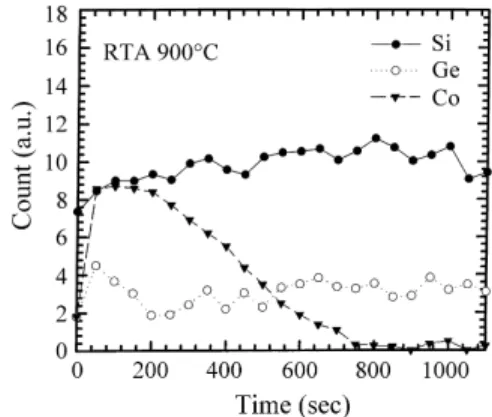
increasing temperature. Fig. 1 shows the AES spectra of Co/poly-Si0.91Ge0.09 sample annealed at 900◦C. In this
fig-ure, TiN capping layer and the unreacted Co film have been removed. As illustrated, the segregated Ge atoms accumu-late in the surface of the sample, and the Ge/Si atomic ratio in the middle of the reacted layer is less than that of the underlying poly-Si1−xGexlayer. This is similar to previous
observation on the reaction of Co and epitaxial-Si1−xGex
[7,12,13]. Because the transformation of CoSi to CoSi2can
Fig. 1. AES spectra after Co annealing on poly-Si0.91Ge0.09 layers at 900◦C.
Fig. 2. Temperature dependence of sheet resistance for various Co/poly-Si1−xGex and Co/poly-Si samples.
only occur when Co diffusion dominates at the interface be-tween the Co and the reacted region, the Ge-rich interfacial layer will act as diffusion barrier, and retard the forma-tion of CoSi2 [7]. This phenomenon is more severe for
Co/poly-Si0.79Ge0.21 sample, so no CoSi2is observed even
after 900◦C annealing. While for Co/poly-Si0.91Ge0.09
sam-ple, CoSi2phase could be identified after 900◦C annealing,
and the main diffraction peaks correspond to (1 1 1), (2 2 0) and (3 1 1) orientations. In addition, the main crystal orien-tations of CoSi2are the same as that of the poly-Si1−xGex
[14]. This indicates that CoSi2 has the tendency to grow
along the underlying poly-Si1−xGexorientation.
Fig. 2 demonstrates the dependence of sheet resistance on the RTA temperatures for Co/poly-Si0.91Ge0.09 and
Co/poly-Si0.79Ge0.21samples. The conventional Co/poly-Si
samples were also measured for comparison. At 500 and 600◦C, the sheet resistance of Co/poly-Si sample is much higher than that of the Co/poly-Si1−xGex sample.
This is probably because of the relatively low resistiv-ity of the CoGe phase. On the other hand, the sheet resistance of the reacted Co/poly-Si1−xGex films after
700 and 800◦C annealing is much higher than that of the Co/poly-Si counterparts. This is believed to be due to the formation of a Ge-rich surface layer by Ge segregation and the high-resistive CoSi growth in Co/poly-Si1−xGex films.
While the low-resistivity CoSi2 phase has already been
formed for Co/poly-Si reaction at these intermediate temper-atures (i.e., 700 and 800◦C), as is confirmed from the X-ray diffraction spectra. In addition, the sheet resistance begins to decrease for Co/poly-Si0.91Ge0.09 with 800◦C annealing,
but the sheet resistance for Co/poly-Si0.79Ge0.21 remains
high. This indicates that the formation of CoSi2 is indeed
retarded in high Ge content samples. This may be due to the decrease of Co or Si diffusion as a result of the Ge accumu-lation at the Co/poly-Si1−xGexreaction interface [7]. While
the sheet resistance of Co/poly-Si0.91Ge0.09 samples is
re-duced to less than 10/䊐after 900◦C annealing, indicating the conversion of CoSi phase to CoSi2 phase, the sheet
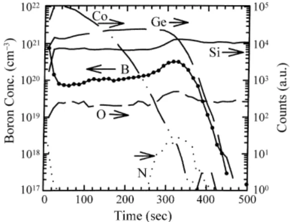
Fig. 3. The SIMS depth profile for Co(10 nm)/poly-Si0.79Ge0.21(200 nm) on nitride/oxide gate dielectric structure after 850◦C RTA annealing.
resistance of Co/poly-Si0.79Ge0.21 sample increases instead
with increasing RTA temperature. As illustrated by X-ray diffraction results, more reduction in Ge content is found in Co(Si1−yGey) phase with increasing RTA temperature.
This leads to the increase of relatively high-resistive CoSi in Co(Si1−yGey) phase. From Fig. 2, the lowest RTA
tempera-ture required to achieve the lowest sheet resistance are∼700, 900, and >900◦C for Co/poly-Si, Co/poly-Si0.91Ge0.09, and
Co/poly-Si0.79Ge0.21, respectively. These values are higher
than those of the Co/epitaxial-Si1−xGex case as found in
our previous experiment, which are∼650, 800, and 800◦C for Co/Si, Co/Si0.91Ge0.09, and Co/Si0.8Ge0.2, respectively
[13]. These results are intriguing, as it indicates that the re-action of Co and Si1−xGexis influenced by the orientation
of the Si1−xGexsubstrate.
For the reaction between Co and heavily boron-doped poly-Si1−xGex, boron may redistribute in the reacted
re-gion during RTA annealing and affect the Co/Si1−xGex
interaction. Fig. 3 shows the SIMS depth profile of Co/poly-Si0.79Ge0.21 sample annealed at 850◦C. Because
of the low solubility of boron in Co silicide [12], the boron atoms could be released from the consumed Si1−xGex
re-gion, and accumulate near the silicide surface, as illustrated in the Fig. 3. It is worthy to note here that, although the boron concentration is reduced within the silicide region, its concentration still remains high enough in the unreacted poly-Si1−xGex(∼ 1 × 1020cm−3) layer. This is extremely
important, as it is necessary to avoid poly-gate depletion effect for poly-Si1−xGex-gated MOS transistor
applica-tions. Furthermore, a weaker surface accumulation of Ge atoms was observed in Fig. 3 than in Fig. 1, this is due to either resolution limitation of SIMS apparatus or the relatively higher Ge content of unreacted films in Fig. 3. In addition, the Ge content near the poly-Si1−xGex/nitride
interface remains essentially unchanged as compared to the as-deposited poly-Si1−xGex film. These features
en-sure that the threshold voltage is well controlled with the incorporation of Co silicidation process.
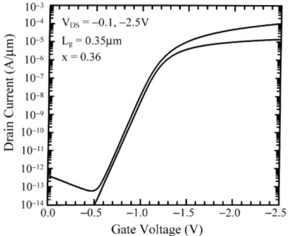
Fig. 4. Transfer characteristics of p-channel MOSFET with Co-salicided poly-Si0.64Ge0.36 gate.
The subthreshold characteristics of a typical p-channel MOS transistor with Co-salicided poly-Si0.64Ge0.36 gate
are shown in Fig. 4. The effective channel length Leff is
0.35m for the device. From the figure, the subthreshold slope is found to be approximately 83 mV dec−1, and the drain-induced barrier lowering (DIBL) is approximately 15 mV V−1. The off-state leakage current is less than 10 pAm−1. These values are essentially the same as those of the device without Co salicidation, an indication that the Co salicidation process does not degrade the device perfor-mance. In addition, we have also measured the gate-drain leakage and its value is found to be less than 0.01 pAm−1, indicating that no bridging occurs between gate and drain (or source). Finally, by comparing the drive current, the de-vice with Co salicide (∼0.102 mA m−1 atVGS= VDS =
−2.5 V) shows a higher drive current than its counterpart
without Co salicide (∼0.093 mA m−1 at VGS = VDS =
−2.5 V). This can be explained by the lower source/drain
sheet resistance (∼15 /䊐, compared to ∼50/䊐 with-out Co salicide). Although the higher sheet resistance of
Fig. 5. The dependence of sheet resistance on line width for Co/Si, Co/poly-Si, and Co/poly-Si0.64Ge0.36 after 850◦C RTA annealing. The thickness of Co was 10 nm.
Co/poly-Si1−xGex gate, compared to Co/poly-Si,does not
affect the DC performance of the device, it may increase the gate delay time. This disadvantage can be overcome by capping a sacrificial Si layer on top of the poly-Si1−xGex
film. In this way, the resultant sheet resistance can be low-ered by about an order of magnitude, as shown in Fig. 5. In addition, the sheet resistances of Co/poly-Si-gate had comparable values with those of Co/Si-source/drain.
4. Conclusion
In this paper, a detailed comparison on the Co reaction with poly-Si0.91Ge0.09 and poly-Si0.79Ge0.21 were studied.
The phase sequence in the reaction of Co with poly-Si0.91
-Ge0.09 is found to be Co(Si1−yGey), CoSi+ CoSi2, and
CoSi2, from 500–700, 800, to 900◦C annealing, respectively.
However, the phase sequence in the reaction of Co with poly-Si0.79Ge0.21 is found to be Co(Si1−yGey), and CoSi
from 500–700, to 800–900◦C annealing, and no CoSi2phase
is found even after high temperature annealing. The retar-dation of the CoSi2phase formation is believed to be due to
the Ge atoms segregated to the upper silicide region and the monosilicide (and disilicide) boundaries, as observed from AES analyses. Because of the retardation of CoSi2phase in
higher Ge content samples, the RTA temperature has to be increased to achieve the desired low sheet resistance, which is not compatible with the trend of low thermal budget. This disadvantage, however, can be overcome by employing a sacrificial poly-Si layer on top of the poly-Si1−xGexfilm for
MOS device fabrication. Finally, we have successfully fab-ricated p-channel poly-Si1−xGex-gated MOSFET with Co
salicide. The device shows an improved drive current with otherwise the same device parameters, as compared to the device without salicide, presumably due to its lower series resistance.
Acknowledgements
The authors would like to thank Dr. F.M. Pan, Dr. W.F. Wu, and Dr. H.C. Lin for experimental assistance. This work was supported in part by the National Science Council of the Republic of China (#NSC89-2215-E009-050).
References
[1] H.C. Lin, T.G. Jung, H.Y. Lin, C.Y. Chang, T.F. Lei, J. Appl. Phys. 74 (1993) 5395.
[2] T.J. King, J.R. Pfiester, J.D. Shott, J.P. McVittie, K.C. Saraswat, IEDM 90 (1990) 253.
[3] K.M. Chen, H.J. Huang, G.W. Huang, C.Y. Chang, L.P. Chen, Jpn. J. Appl. Phys. 38 (1999) L1099.
[4] L. van den Hove, R. Wolters, K. Maex, R. de Keersmaecker, G.J. Declerck, IEEE Trans. Electron. Dev. ED-34 (1987) 554.
[6] L. van den Hove, R. Wolters, K. Maex, R. de Keersmaecker, G.J. Declerck, J. Vac. Sci. Technol. B 4 (1986) 1358.
[7] M. Glück, A. Schüppen, M. Rösler, W. Heinrich, J. Hersener, U. König, O. Yam, C. Cytermann, M. Eizenberg, Thin Solid Films 270 (1995) 549.
[8] K. Prabhakaran, K. Sumitomo, T. Ogino, Surf. Sci. 421 (1999) 100. [9] Z. Wang, D.B. Aldrich, Y.L. Chen, D.E. Sayer, R.J. Nemanich, Thin
Solid Films 270 (1995) 555.
[10] P.T. Goeller, B.I. Boyanov, D.E. Sayers, R.J. Nemanich, Nucl. Instrum. Meth. Phys. Res. B 133 (1997) 84.
[11] J.S. Luo, W.T. Lin, C.Y. Chang, W.C. Tsai, S.J. Wang, Mater. Chem. Phys. 48 (1997) 140.
[12] C. Cytermann, E. Holzman, R. Brener, M. Fastow, M. Eizenberg, M. Glück, H. Kibbel, U. König, J. Appl. Phys. 83 (1998) 2019.
[13] H.J. Huang, K.M. Chen, C.Y. Chang, T.Y. Huang, T.C. Chang, L.P. Chen, G.W. Huang, J. Vac. Sci. Technol. A 18 (2000) 1448. [14] K.M. Chen, H.J. Huang, L.P. Chen, G.W. Huang, C.Y. Chang, in:
Proceedings of the 46th International Symposium, American Vacuum Society, Seattle, 1999.