On-Chip High-Voltage Charge Pump Circuit in
Standard CMOS Processes With Polysilicon Diodes
Ming-Dou Ker and Shih-Lun Chen Nanoelectronics and Gigascale Systems Laboratory
Institute of Electronics, National Chiao-Tung University, Hsinchu, Taiwan Abstract—An on-chip high-voltage charge pump circuit
realized with the polysilicon diodes in standard (bulk) CMOS process is presented in this paper. Because the polysilicon diodes are fully isolated from the substrate, the output voltage of the charge pump circuit is not limited by the junction breakdown voltage of MOSFETs. The polysilicon diodes can be implemented in the standard CMOS processes without extra process steps. The proposed charge pump circuit has been fabricated in a 0.25-µm 2.5-V standard CMOS process. The output voltage of the 12-stage charge pump circuit can be pumped up to 28.08 V, which is much higher than the n-well/p-substrate breakdown voltage (18.9 V) in a 0.25-µm 2.5-V standard CMOS process.
I. INTRODUCTION
Charge pump circuits can generate the dc voltages those are higher than the normal power supply voltage (VDD) or lower than the ground voltage (GND). Charge pump circuits are usually applied to the nonvolatile memories, such as EEPROM and flash memories, to write or to erase the floating-gate devices [1], [2]. Besides, charge pump circuits can be also used in some low-voltage designs to improve the circuit performance [3]. In the MEMS applications, the charge pump circuit must provide the output voltage higher than 15 V, even to 60 V [4], [5]. Early, the pn-junction diodes were used in the charge pump circuit. Then, Dickson reported the charge pump circuit by using the diode-connected devices [6]. Due to the body effect, the pumping efficiency of the Dickson charge pump circuit is degraded as the number of the stages increases. Several modified charge pump circuits based on the Dickson charge pump circuit were reported to enhance the pumping efficiency [7]-[10].
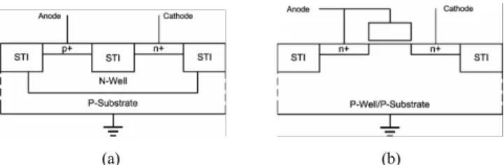
As the semiconductor process is scaled down, the normal operation voltage also decreased due to the reliability issue [11]. Thus, the reliability issue must be considered to design the charge pump circuit in the deep-sub-micron process, such as gate-oxide reliability problem [10]. Figure 1(a) shows the cross section of the p+/n-well diode in the grounded p-substrate. The p+/n-well diode is one kind of the pn-junction diodes in standard (bulk) CMOS process. In Figure 1(a), a parasitic pn-junction is between the n-well and the grounded p-type substrate. If the voltage on the cathode of the
p+/n-well diode is larger than the junction breakdown voltage between the n-well and the grounded p-substrate, the charges on the cathode will leak to ground through the parasitic junction. Figure 1(b) shows the cross section of the diode-connected NMOS, whose gate and drain are diode-connected together, in the grounded p-substrate. In Figure 1(b), an undesired pn-junction parasitizes between the n+ region (source/drain) and the grounded p-substrate. Similarly, if the voltages on the cathode or anode of the diode-connected NMOS are larger than the junction breakdown voltage between the n+ region (source/drain) and the grounded p-substrate, the charges on the cathode or anode will also leak to ground through the parasitic junction. Hence, whenever the p+/n-well (pn-junction) diodes or the diode-connected devices are used to design the charge pump circuit, the output voltage will be limited by the breakdown voltage of the undesired junction in standard CMOS process. In the SOI (silicon-on-insulator) process, the charge pump circuits can pump the output voltage higher without the limitation of the parasitic pn-junctions because the devices in the SOI CMOS process are isolated to others by the insulator layer [4], [5]. However, the SOI CMOS process is more expensive than the standard (bulk) CMOS process.
(a) (b)
Figure 1. Schematic cross sections of (a) the p+/n-well diode, and (b) the diode-connected NMOS, in grounded p-type substrate.
In this paper, an on-chip high-voltage charge pump circuit realized with the polysilicon diodes is proposed. Because the anode and the cathode of the polysilicon diodes are fully isolated from the substrate, the voltages on the anode or the cathode of the polysilicon diodes are not limited by the breakdown voltage of the undesired parasitic pn-junction. The proposed on-chip high-voltage charge pump circuit with the polysilicon diodes has been implemented and successfully verified in a 0.25-μm 2.5-V standard (bulk) CMOS process.
6-4
157
II. POLYSILICON DIODES
A. Structure of the Ploysilicon Diodes
In the previous standard CMOS processes, the gates of PMOS and NMOS are both realized with the n-type doped polysilicon. Because of the work function consideration, the gate of PMOS and the gate of NMOS are realized with the p-type doped polysilicon and the n-p-type doped polysilicon in the recent sub-quarter-micron CMOS processes, respectively. In order to implement the different types of polysilicon gates, the intrinsic polysilicon layer is deposited first, and then the p-type and n-type impurities are doped into the intrinsic polysilicon layer to form the PMOS gate and the NMOS gate, respectively. So, the diode can be realized on the polysilicon layer by recent standard CMOS processes those have separated doping impurities for PMOS and NMOS.
Figure 2 shows the cross section of the polysilicon diode in the standard CMOS process. As shown in Figure 2, the STI (shallow trench isolation) layer is located above the silicon substrate. The polysilicon layer is deposited on the STI layer. Then, the p-type and n-type highly doped regions on the polysilicon are doped with the same process of the PMOS and NMOS source/drain implement, respectively. Thus, the polysilicon diode is fully process compatible to the standard CMOS process without any extra process modification. Because the polysilicon diode is formed on the STI layer, it is isolated from the silicon substrate. Thus, the charges on the anode and the cathode of the polysilicon diode don’t leak to the silicon substrate. In the polysilicon diode, an extra un-doped (intrinsic) polysilicon region (i) can be inserted between the p-type and n-type doped polysilicon regions. The length (Lc) of the un-doped center region can be used to adjust the I-V characteristics of the polysilicon diode.
Figure 2. Schematic cross section of the polysilicon diode in the standard (bulk) CMOS process.
B. Characteristics of the Polysilicon Diodes
The polysilicon diodes with different lengths (Lc) of the un-doped center region have been fabricated in a 0.25-µm 2.5-V standard CMOS process, where the Lc is changed from 0.25 µm to 1.5 µm. Figure 3 shows the measured I-V curves of the polysilicon diodes with different Lc. Figure 4 shows the measured cut-in voltages of the polysilicon diodes with different Lc, where the cut-in voltages are defined at the 1-µA forward biased current. In Figure 4, the cut-in voltages of these polysilicon diodes vary from 0.47 V to 0.58 V. As the length of the un-doped region is larger than 0.9 µm, the cut-in voltage saturates at around 0.58 V.
Figure 3. Measured I-V curves of the polysilicon diodes with different lengths (Lc) of the un-doped center region.
Figure 4. Measured cut-in voltages of the polysilicon diodes with different lengths of the un-doped center region. The cut-in voltages are defined at the 1-µA forward biased current.
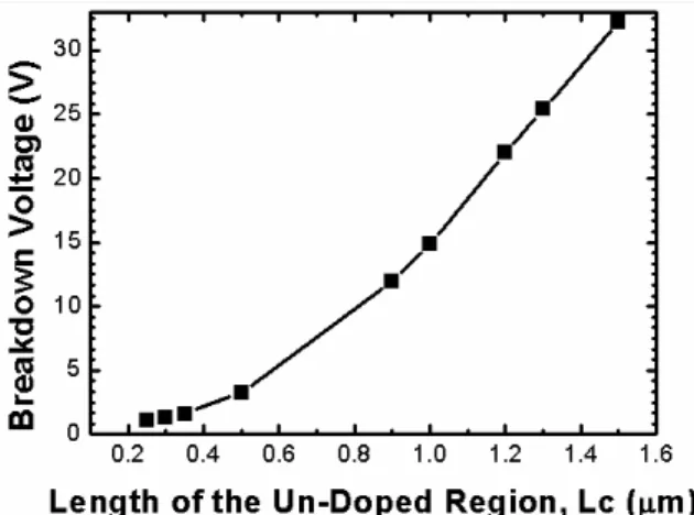
Figure 5. Measured reverse breakdown voltages of the polysilicon diodes with different lengths of un-doped center region. The reverse breakdown voltages are defined at the 1-µA reverse biased current.
Figure 5 shows the measured reverse breakdown voltages of the polysilicon diodes with different Lc, where the reverse breakdown voltages are defined at the 1-µA reverse biased current. In Figure 5, the reverse breakdown voltage increases when the Lc increases. As the Lc is larger than 1.2 µm, the reverse breakdown voltage is larger than 20 V. Moreover, 158
the reverse breakdown voltage is 33 V when the length of the un-doped region is 1.5 µm. Hence, the reverse breakdown voltage of the polysilicon diode can be adjusted by changing the length of the un-doped center region for different applications.
III. CHARGE PUMP CIRCUIT WITH POLYSILICON DIODES
A. Charge Pump Circuit
Figure 6 shows the 4-stage charge pump circuit designed with 5 polysilicon diodes (D1~D5), where the clock signals, CLK and CLKB, are out-of-phase and with the amplitude of VDD (2.5 V). In Figure 6, the RL and CL represent the output loading of resistance and capacitance, respectively. The CL can make the output voltage more stable. If the parasitic capacitance at each node and the output current through the RL can be ignored, the ideal output voltage of the charge pump circuit can be expressed as
Vout = (n + 1) × (VDD – VD), (1)
where VD is the cut-in voltage of the polysilicon diode and n
is the number of stages in the charge pump circuit. Thus, as the number of stages increases, the output voltage of the charge pump circuit is also increased.
Figure 6. 4-stage charge pump circuit realized with 5 polysilicon diodes.
B. Experimental Results
In the testchip, the 4-stage, 8-stage, and 12-stage charge pump circuits with 10-pF on-chip pumping capacitors and the polysilicon diodes having 0.5-µm and 1-µm un-doped region have been fabricated in a 0.25-µm 2.5-V standard (bulk) CMOS process. Figure 7 shows the photograph of the 4-stage charge pump circuit with the polysilicon diodes (Lc=0.5 µm). The independent polysilicon diodes with different length of the un-doped region are also implemented in this testchip.
Figure 7. Photograph of the 4-stage charge pump circuit (Lc=0.5 µm) fabricated in a 0.25-µm 2.5-V standard (bulk) CMOS process.
Figure 8 shows the measured waveforms of the 12-stage charge pump circuit with the polysilicon diodes (Lc=0.5 µm) to drive the capacitive output load. In Figure 8, the power supply voltage and the amplitude of the clock signals (CLK
and CLKB) are 2.5 V, and the clock frequency is 1 MHz. As shown in Figure 8, the output voltage of the charge pump circuit to drive the capacitive load is as high as 28.08 V, which is much higher than the n-well/p-substrate breakdown voltage (18.9 V) in the given 0.25-µm 2.5-V standard CMOS process.
Figure 8. Measured waveforms of the 12-stage charge pump circuit with the polysilicon diodes (Lc=0.5 µm) to drive capacitive output load. The clock frequency is 1 MHz and the power supply voltage (VDD) is 2.5 V.
Figure 9 shows the measured output voltages of the 4-stage, 8-4-stage, and 12-stage charge pump circuits with the polysilicon diodes having 0.5-µm or 1-µm un-doped center region (Lc). In Figure 9, the proposed charge pump circuits drive only the capacitive loads with the clock frequency of 1 MHz and the power supply voltage (VDD) of 2.5 V. As shown in Figure 9, the measured output voltages of the charge pump circuits with the polysilicon diodes (Lc=0.5 or 1 µm) are almost the same. The length of the un-doped region (Lc) doesn’t obviously affect the output voltage of the proposed charge pump circuit because the voltage across each polysilicon diode doesn’t exceed VDD (2.5 V), which is smaller than the reverse breakdown voltages of the polysilicon diodes (Lc=0.5 or 1 µm).
Figure 9. Measured output voltages of the 4-stage, 8-stage, and 12-stage charge pump circuits with the polysilicon diodes having 0.5-µm and 1-µm un-doped region to drive capacitive load. The clock frequency is 1 MHz and the power supply voltage (VDD) is 2.5 V.
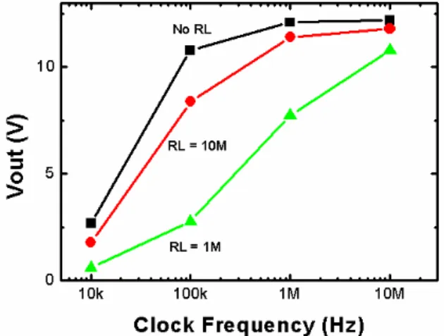
Figure 10 shows the measured output voltages of the 4-stage, 8-4-stage, and 12-stage charge pump circuits with the polysilicon diodes (Lc=1 µm) to drive different output resistors (RL). In Figure 10, the clock frequency is 1 MHz and the power supply voltage (VDD) is 2.5 V. If the RL is large, the output current is small. As shown in Figure 10, the output voltage is degraded when the RL is reduced. As the RL is 10 MΩ, the output voltage of the 12-stage charge pump circuit can be still higher than 20 V, which implies a loading current of ~2 µA.
Figure 10. Measured output voltages of the 4-stage, 8-stage, and 12-stage charge pump circuits (Lc=1 µm) with the output loading of 1 MΩ, 10 MΩ, or without the output resistor. The clock frequency is 1 MHz and the power supply voltage (VDD) is 2.5 V.
Figure 11 shows the measured output voltages of the 4-stage charge pump circuit with the polysilicon diodes (Lc=1 µm) under different clock frequencies, where the power supply voltage (VDD) is 2.5 V. When the clock frequency is increased, the output voltages of the charge pump circuit are also increased. But, when the clock frequency is low, the output voltages of the charge pump circuit are degraded, especially with small RL. In Figure 11, the charge pump circuit can pump the output voltage close to the ideal value in (1) when the RL is large and the clock frequency is high.
Figure 11. Measured output voltages of the 4-stage charge pump circuit (Lc=1 µm) with the output loading of 1 MΩ, 10 MΩ, or without the output resistor under different clock frequencies. The power supply voltage (VDD) is 2.5 V.
IV. CONCLUSION
On-chip high-voltage charge pump circuit realized with the polysilicon diodes has been successfully verified in a 0.25-µm 2.5-V standard (bulk) CMOS process. The polysilicon diodes are formed on the STI layer, which are isolated from the substrate. Thus, the output voltage of the charge pump circuit with the polysilicon diodes isn’t limited by the junction breakdown voltage. Besides, the polysilicon diodes are fully process compatible to the standard CMOS processes without any extra process modification. The 4-stage, 8-4-stage, and 12-stage charge pump circuits with 10-pF on-chip pumping capacitors and the polysilicon diodes having 0.5-µm and 1-µm un-doped center region have been fabricated in a 0.25-µm 2.5-V standard (bulk) CMOS process. To drive the capacitive load, the measured results show that the 12-stage charge pump circuit with the polysilicon diodes (Lc=0.5 µm) can pump the output voltage as high as 28.08 V. The loading effect and the dependence of clock frequency on the output voltage of the proposed charge pump circuit are also measured in this work. By using the polysilicon diodes, the negative charge pump circuit can be also implemented in the standard CMOS processes without the limitation of the junctions.
REFERENCES
[1] T. Kawahara, T. Kobayashi, Y. Jyouno, S.-I. Saeki, N. Miyamoto, T. Adachi, M. Kato, A. Sato, J. Yugami, H. Kume, and K. Kimura, “Bitline clamped sensing multiplex and accurate high voltage generator for quarter-micron flash memories,” IEEE J. Solid-State
Circuits, vol. 31, pp. 1590–1600, Nov. 1996.
[2] T. Tanzawa, Y. Takano, K. Watanabe, and S. Atsumi, “High-voltage transistor scaling circuit techniques for high-density negative-gate channel-erasing NOR flash memory,” IEEE J. Solid-State Circuits, vol. 37, pp. 1318–1325, Oct. 2002.
[3] R. S. Pierre, “Low-power BiCMOS op-amp with integrated current-mode charge pump,” IEEE J. Solid-State Circuits, vol. 35, pp. 1046– 1050, Jul. 2000.
[4] M. R. Hoque, T. McNutt, J. Zhang, A. Mantooth, and M. Mojarradi, “A high voltage Dickson charge pump in SOI CMOS, in Proc. IEEE
Custom Integrated Circuits Conf., 2003, pp. 493–496.
[5] M. R. Hoque, T. Ahmad, T. McNutt, A. Mantooth, and M. Mojarradi, “Design technique of an on-chip, high-voltage charge pump in SOI,” in Proc. IEEE Symp. Circuits Syst., 2005, pp. 133–136.
[6] J. F. Dickson, “On-chip high-voltage generation in MNOS integrated circuits using an improved voltage multiplier technique,” IEEE J.
Solid-State Circuits, vol. 11, pp. 374–378, Jun. 1976.
[7] K.-H. Choi, J.-M. Park, J.-K. Kim, T.-S. Jung, and K.-D. Suh, “Floating-well charge pump circuits for sub-2.0V single power supply flash memories,” in Symp. VLSI Circuits Dig. Tech. Papers, 1997, pp. 61–62.
[8] J.-T. Wu and K.-L. Chang, “MOS charge pump for low-voltage operation,” IEEE J. Solid-State Circuits, vol. 33, pp. 592–597, Apr. 1998.
[9] J. Shin, I.-Y. Chung, Y. J. Park, and H. S. Min, “A new charge pump without degradation in threshold voltage due to body effect,” IEEE J.
Solid-State Circuits, vol. 35, pp. 1227–1230, Apr. 2000.
[10] M.-D. Ker, S.-L. Chen, and C.-S. Tsai, “A new charge pump circuit dealing with gate-oxide reliability issue in low-voltage processes,” in
Proc. IEEE Int. Symp. Circuits Syst., 2004, vol. I, pp. 321–324.
[11] Semiconductor Industry Association, International Technology
Roadmap for Semiconductors, 2004.