國 立 交 通 大 學
電機與控制工程學系
碩士論文
生醫應用之解析度可調變ΣΔ類比數位轉換器
Sigma-Delta ADC with Configurable Resolution and Bandwidth
for Biomedical Applications
研究生:張孟修
指導教授:林進燈 博士
生醫應用之解析度可調變ΣΔ類比數位轉換器
Sigma-Delta ADC with Configurable Resolution and Bandwidth
for Biomedical Applications
研究生:張孟修
Student: Meng-Siou Jhang
指導教授:林進燈 博士 Advisor:
Dr.
Chin-Teng
Lin
國立交通大學
電機與控制工程學系
碩士論文
A Thesis
Submitted to Department of Electrical and Control Engineering College of Electrical Engineering
National Chiao Tung University in Partial Fulfillment of the Requirements
for the Degree of Master in
Electrical and Control Engineering July 2008
Hsinchu, Taiwan, Republic of China
生醫應用之解析度可調變ΣΔ類比數位轉換器
學生:張孟修
指導教授:林進燈 博士
國立交通大學電機與控制工程研究所
中文摘要
本論文的研究提出一個可依選擇的模式而改變解析度的三角積分類比數位轉 換器,總共分為二種模式可供選擇,此二種模式依不同的輸入訊號而有不同需求 的解析度,一為生理電訊號,一為生理影像訊號。則在生理電訊號和生理影像訊 號的擷取系統中,透過後端的控制來轉換不同解析度的模式,達到不同通道共用一顆ADC 的設計以結省整體系統面積和功耗。ADC 的架構選用 Sigma-Delta 的
架構,主要分為二個部分:三角積分模組和後端的降頻數位濾波器。
此ADC 電路操作在 1.28MHz 的操作頻率,訊號取樣頻率為 640kHz,對生理
電訊號而言,超取樣率為256;對生理影像訊號而言,超取樣率為 32。整個 ADC
電路的輸出為 SPI bus 標準介面輸出,使此電路可直接和後端的運算電路(DSP)
作溝通。且使用低電壓源1.5V 的電壓供應,最後結果為在生理電訊號的模式時,
SNDR 為 60dB,ENOB 為 10-bit;在生理影像訊號模式時,SNR 為 50dB,ENOB
為 8-bit。此電路實現使用 TSMC 0.18-um 1P6M CMOS 製程,整體電路功耗
14.2mW,其中 Sigma-Delta modulator 的功耗為 0.98 mW;數位降頻濾波器和其
餘數位控制電路功耗為13.3 mW,其晶片大小為 3.21mm2。
關鍵字:生理電訊號,生理影像訊號,三角積分調變器,二種模式,低電壓供應, SPI 介面,CIC filter,HB filter。
Sigma-Delta ADC with Configurable Resolution and Bandwidth for
Biomedical Applications
Student: Meng-Siou Jhang
Advisor: Dr. Chin-Teng Lin
Department of Electrical and Control Engineering
National Chiao Tung University
Abstract
This paper presents a Sigma-Delta ADC which can change resolutions when the type of the input signal is different. This ADC provides two modes. One is designed for bio-electric signals; the other is designed for bio-image signals. This ADC can change its resolution by the control unit of a multi-channel design for bio-electric and bio-image signal through SPI. It includes two parts: Sigma-Delta modulator and decimation filter.
The proposed ADC operates at 1.28 MHz. Sampling rate is 640 kHz. For bio-electric signals, oversampling rate (OSR) is 256; for bio-image signals, OSR is 32. The ADC communicates with DSP or other devices by SPI bus. In the bio-electric signal mode, SNR is 50dB, effective number of bits (ENOB) is 10-bit; in the bio-image signal mode SNR is 50dB, ENOB is 8-bit. It has been fabricated by TSMC 0.18 μm CMOS 1P6M standard process. The total power consumption of the chip is about 14.4 mW under 1.5V supply, and the power consumption of Sigma-Delta modulator is about 0.98 mW; the power consumption of digital part is 13.3 mW. The area of the chip is 3.21 mm2.
Keyword: Bio-electric signal, Bio-image signal, Sigma-Delta ADC, Configurable, low voltage supply, SPI bus, CIC filter, HB filter.
誌
謝
本論文的完成,首先要感謝指導教授林進燈博士這兩年來的悉心指導,讓我 學習到許多寶貴的知識,在學業及研究方法上也受益良多。另外也要感謝口試委 員們的的建議與指教,使得本論文更為完整。 其次,感謝協助指導資訊媒體實驗室的鍾仁峯博士、范倫達博士,腦中心的 柯立偉博士,在理論及實作技巧上給予我相當多的幫助與建意,讓我獲益良多。 此外,也衷心感謝學長姐紹航、俊傑、德瑋、智文、吉隆、真如及靜瑩,同學煒 忠、寓鈞、舒凱、孟哲、依伶、建昇、毓婷及儀晟的相互砥礪,以及學弟妹昕展、 哲睿、介恩、有德及家欣在研究過程中所給我的鼓勵與協助。 感謝我的父母親張永宗先生和何雲琴女士對我的教育與栽培,並給予我精神 及物質上的一切支援,使我能安心地致力於學業。此外也感謝弟弟張孟哲對我不 斷的關心與鼓勵。 謹以本論文獻給我的家人及所有關心我的師長與朋友們。Contents
中文摘要...ii Abstract... iii 誌 謝...iv Contents ...v List of Tables...viiList of figures... viii
Chapter 1 Introduction...1
1 - 1 Motivation ...2
1 - 2 Oversampling-rate ADC and Nyquist-rate ADC ...3
1 - 3 Organization of the thesis ...6
Chapter 2 Theorem of Sigma-Delta ADC and Related Research...7
2 - 1 Theorem of Sigma-Delta Modulator ...7
2 -1 - 1 Quantization ...9
2 -1 - 2 Oversampling ...10
2 -1 - 3 Performance Metrics ...10
2 -1 - 4 The Concept of Sigma-Delta ADC...12
2 - 2 Digital Decimation FIR Filter...14
2 - 2 - 1 Decimation ...14
2 - 2 - 2 FIR Filter...17
2 - 3 CIC (Cascaded Integrator-Comb) Filter ...19
2 - 3 - 1 Building Blocks...19
2 - 3 - 2 Frequency Characteristics ...22
2 - 3 - 3 Bit Growth...24
2 - 3 - 4 Implementation Details ...25
2 - 3 - 5 Sharpened CIC Filters ...26
2 - 4 Relative Architecture Survey...26
2 - 4 - 1 Very Low-Voltage Digital-Audio ΔΣ Modulator with 88-dB Dynamic Range Using Local Switch Bootstrapping ...27
2 - 4 - 2 Cascaded ΣΔ ADC for ADSL2+ Application...28
2 - 4 - 3 A Reconfigurable A/D Converter for 4G Wireless System...30
Chapter 3 System Architecture...32
3 - 1 Architecture of Sigma-Delta ADC ...33
3 - 2 Behavior Simulation of Sigma-Delta Modulator...34
3 - 2 - 2 Simulation in Bio-Image Signal Mode...39
3 - 3 Architecture and Design of Sigma-Delta Modulator...41
3 - 3 - 1 Non-overlap Clock Generator ...41
3 - 3 - 2 Bootstrapped Switch ...43
3 - 3 - 3 Comparator...46
3 - 3 - 4 Operation Amplifier ...49
3 - 4 2nd-Order Sigma-Delta Modulator...55
3 - 5 Design of Digital Decimation Filters...58
3 - 5 - 1 Low Power Design of CIC Filter ...59
3 - 5 - 2 Design of HB Filter...67
3 - 5 - 3 Simulation Result ...71
3 - 6 Design of SPI Bus...72
Chapter 4 Realization and Layout of Whole Chip and Testing Consideration.73 4 - 1 Design Flow...73
4 - 2 Layout and Post Simulation of Sigma-Delta Modulator ...75
4 - 3 Layout and Post Simulation of Sigma-Delta ADC...76
4 - 4 Testing Consideration ...81 Chapter 5 Conclusions...83 References...85 Appendix...88 A DRC Verification...88 B LVS Verification...89
C Tapeout Review Form ...91
1.Tapeout review form (for Full-custom IC) ...91
2.Tapeout Review Form (for Cell-Based IC)...94
List of Tables
Table 1: Different architectures of ADC. ...4
Table 2: Modulator Transfer Functions...31
Table 3: Specifications of 2nd-order Sigma-Delta modulator ...35
Table 4: The specifications of opamp and comparator. ...55
Table 5: Truth table of a x n11 ( −11)+a x n49 ( −49). ...65
Table 6: Specifications of the four stages decimation filter...67
Table 7: Approximated parameters of the four stage HB filters. ...69
Table 8: Specifications of this ADC...80
List of figures
Figure 1 - 1: A signal analyzing system. ...1
Figure 1 - 2: Multi-channel architecture. ...2
Figure 1 - 3: Block diagram of EEG/EKG/EOG/EMG/fNIRS multi-sensor platform..3
Figure 1 - 4: (a) Nyquist-rate and (b) Oversampling-rate ADC architecture...5
Figure 1 - 5: Spectrum (a) Nyquist-rate ADC (b) Oversampling-rate ADC...5
Figure 2 - 1: The operation diagram of ADC...8
Figure 2 - 2: Spectrum of signal after sampling. ...9
Figure 2 - 3: (a) Basic block diagram of a Sigma-Delta modulator (b) block diagram of Sigma-Delta modulator in Z-domain...13
Figure 2 - 4: Spectrum of different L of |NTF|...14
Figure 2 - 5: Spectrum when the sampling date is decimate twice...15
Figure 2 - 6: Spectrum with aliasing versus spectrum of anti-aliasing...16
Figure 2 - 7: (a) direct architecture and (b) transfer-direct architecture of FIR filter. .17 Figure 2 - 8: Linear phase architecture of N-tap FIR filter, (a) when N is even and (b) N is odd...18
Figure 2 - 9: Basic Integrator. ...20
Figure 2 - 10: Basic Comb filter. ...22
Figure 2 - 11: Three Stage Decimating CIC Filter...22
Figure 2 - 12: Three Stage Interpolating CIC Filter. ...22
Figure 2 - 13: Fully differential low-voltage integrator. ...27
Figure 2 - 14: Transistor-level implementation of the bootstrapped switch. ...28
Figure 2 - 15: Block diagram of RMASH 2-1-11.5b. ...29
Figure 2 - 16: Circuit implementation of the first-stage modulator. ...29
Figure 2 - 17: Block diagram of proposed architecture. ...30
Figure 3 - 1: Block diagram of this Sigma-Delta ADC. ...33
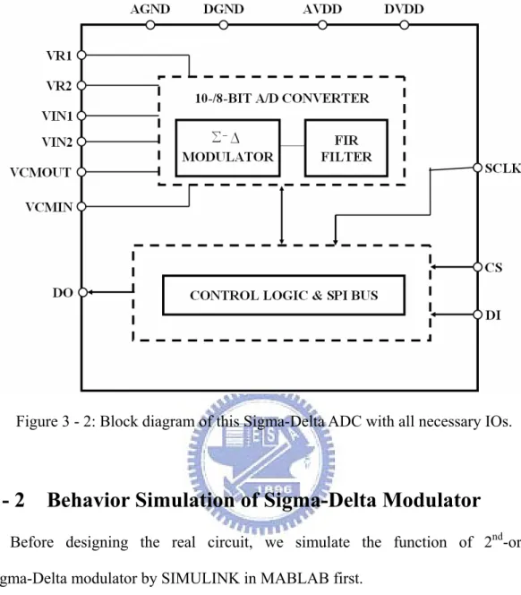
Figure 3 - 2: Block diagram of this Sigma-Delta ADC with all necessary IOs. ...34
Figure 3 - 3: Bandwidth of bio-electric signals. ...35
Figure 3 - 4: Block diagram of a 2nd-order Sigma-Delta modulator. ...36
Figure 3 - 5: Flow diagram of 2nd-order Sigma-Delta modulator. ...36
Figure 3 - 6: Waves of four nodes of Sigma-Delta modulator: (a) input (b) output of the first integrator (c) output of the second integrator (d) output of quntizer. ...38
Figure 3 - 8: SNDR versus input lever in bio-electric signal mode...39
Figure 3 - 9: Waves of four nodes of Sigma-Delta modulator: (a) input (b) output of the first integrator (c) output of the second integrator (d) output of quntizer. ...40
Figure 3 - 10: Spectrum of output in bio-image signal mode. ...40
Figure 3 - 11: SNDR versus input level in bio-image signal mode. ...41
Figure 3 - 12: Four non-overlap clocks...42
Figure 3 - 13: Circuit of clock generator...42
Figure 3 - 14: Simulation result of clock generator. ...43
Figure 3 - 15: Gon of nmos, pmos and bootstrapped switch versus input voltage when (a) VDD=3V (b) VDD=1V...43
Figure 3 - 16: (a) circuit of bootstrapped switch (b) during clkb phase (c) during clk phase. ...44
Figure 3 - 17: Transistor level implementation of the bootstrapped switch. ...45
Figure 3 - 18: Simulation result of bootstrapped switch...45
Figure 3 - 19: The SNDR versus input level (a) in bio-electric mode (b) in bio-image mode when offset voltage is 0V and 15mV. ...46
Figure 3 - 20: Circuit of comparator. ...47
Figure 3 - 21: Simulation results of testing of the comparator. (a) first pattern (b) second pattern (c) third pattern. ...48
Figure 3 - 22: the output of the first integrator which is simulated by simulink. ...49
Figure 3 - 23: Inverse integrator with single end...50
Figure 3 - 24: The SNDR with infinite dc gain and gain of 73.3 db versus input level. (a) in bio-electric signal mode (b) in bio-image signal mode...51
Figure 3 - 25: Circuit of opamp. ...51
Figure 3 - 26: Frequency response of opamp...52
Figure 3 - 27: Frequency responses of opamp when voltage supply is 1.5V±10% (1.35 V ~ 1.65 V) and temperature is 0DC~ 90DC...53
Figure 3 - 28: Testing circuit...54
Figure 3 - 29: Output of testing circuit when Vid is a 20 kHz sine wave with 1.5 V Vp-p. ...54
Figure 3 - 30: Output of testing circuit when Vid is a square wave...54
Figure 3 - 31: Circuit of the 2nd-order Sigma-Delta modulator. ...56
Figure 3 - 32: (a) CDS (Correlated Double Sampling) integrator (b) in
Φ
1 phase (c) inΦ
2 phase...57Figure 3 - 33: The simulation result of 2nd-order Sigma-Delta modulator...58
Figure 3 - 35: the spectrum of original CIC filter versus the spectrum of CIC filter
compensated by (a) Sine filter (b) Sine filter and Cosine filter. ...61
Figure 3 - 36: The simplified architecture: a x n0 ( )+a x n1 ( − +1) a n2( − +2) a x n15 ( −15). ...63
Figure 3 - 37: The 17 registers after simplifying operations...64
Figure 3 - 38: The architecture of a x n11 ( −11)+a x n49 ( −49)...65
Figure 3 - 39: Architectures of whole operations which use the second way. ...66
Figure 3 - 40: Spectrum of the ideal filter and filter with approximate parameters (a) the 1st stage HB filter (b) the 2nd and 3rd one (c) the 4th one. ...70
Figure 3 - 41: Block diagram of decimation filter by simulink. ...71
Figure 3 - 42: Simulation result of decimation. ...72
Figure 3 - 43: SPI of CPOL = 1 and CPHA = 1...72
Figure 4 - 1: Design flow of Sigma-Delta modulator. ...74
Figure 4 - 2: Design flow of digital part. ...74
Figure 4 - 3: Layout of Sigma-Delta modulator, additionally, 1, 2 are opamp circuits; 3 is bias circuit; 4 is comparator circuit; 5 is clock generator circuit; 6 is switch circuit; 7 is capacitor array...75
Figure 4 - 4: Post simulation result of Sigma-Delta modulator. ...76
Figure 4 - 5: Layout of whole chip. ...76
Figure 4 - 6: The ADC output in bio-electric signal mode. ...77
Figure 4 - 7: Ideal output wave versus the output of real design...78
Figure 4 - 8: Spectrum of the output of the first test...78
Figure 4 - 9: The ADC Output in bio-image signal mode. ...79
Figure 4 - 10: Ideal output wave versus the output of real design...79
Figure 4 - 11: Spectrum of the output of the second test. ...80
Figure 4 - 12: Testing platform. ...82
Figure B - 1: The information of LVS verification of the analog part...89
Figure B - 2: The information of LVS verification of the whole chip ...90
Figure D - 1: SPI bus with single slave and single master...98
Figure D - 2: A typical hardware setup using two shift registers to form an inter-chip circular buffer...100
Figure D - 3: A timing diagram showing clock polarity and phase ...100
Figure D - 4: CPOL and CPHA of four modes of SPI bus ...101
Chapter 1
Introduction
Architecture of a normal signal analyzing system is shown in Figure 1-1. Usually it includes a front end circuit, analog-to-digital converter (ADC) and operational unit, like DSP. The output of signal analyzing system will be the calculation result depending on different applications. Nowadays, system designed for biomedical application is more and more important. And these biomedical signals like Electroencephalogram (EEG) have to be analyzed by multi-channel inputs.
Figure 1 - 1: A signal analyzing system.
A multi-channel system architecture is shown in Figure 1-2. This is a normal and easy way to implement the system. The circuit of each channel is the same as other channels. And the communication interface will be connected between the sensors and operation unit, like digital signal processor (DSP). When the channel number is big, the cost such as power consumption and chip area will increase. So developing a
architecture to decrease the cost of multi-channel system is required. This research presents a ADC architecture with two modes which can be chosen when the input signal is different. The motivation will be introduced as follows.
Figure 1 - 2: Multi-channel architecture.
1 - 1 Motivation
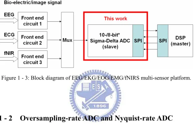
The block diagram of Electro-encephalogram(EEG) / Electro-cardiogram(ECG) / Electro-oculogram(EOG) / Electro-myogram(EMG) / functional near-infrared imaging (fNIR) multi-sensor platform is shown in Figure 1-3. We use three channels as example. There are three channels in the front of this system. A 3-to-1 multiplexer which can choose channel is beyond them. And Sigma-Delta ADC which will be introduced in this paper is between the multiplexer and DSP which can analyzes the signal. This ADC not only converts the analog signal to digital signal but can change the resolution by different signal applications. And the interface between ADC and DSP is a standard SPI bus. This architecture as Figure 1-3 can decrease the cost of the
system. The mode can be chosen by DSP. The ADC provides two modes can be chosen. One is designed for bio-electric signal which likes EEG, EKG, EOG and EMG; the other one is designed for bio-image signal which likes fNIR. But why do we chose Sigma-Delta ADC to implement? The discuss is describe as follows.
Figure 1 - 3: Block diagram of EEG/EKG/EOG/EMG/fNIRS multi-sensor platform.
1 - 2 Oversampling-rate ADC and Nyquist-rate ADC
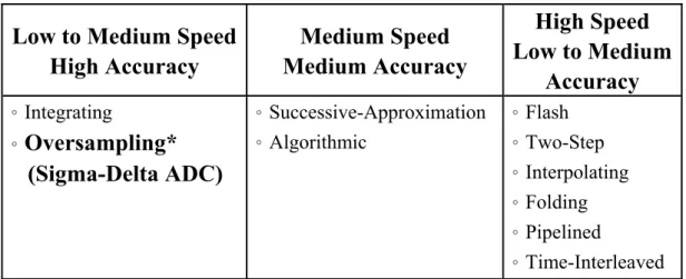
There are several kinds of analog-digital converters in different applications. Usually, the ADC with high resolution and high speed is desired. But high resolution and high speed is not easy to be satisfied at the same time. The speed and resolution will be considered by different applications. According to the way of sampling, we can divide the ADC into two types of ADC. One is Nyquist-rate ADC, and the other one is Oversampling-rate ADC [18][19]. The different ADCs are divided by speed and accuracy as shown in Table 1 [20].
Table 1: Different architectures of ADC.
Low to Medium Speed
High Accuracy
Medium Speed
Medium Accuracy
High Speed
Low to Medium
Accuracy
。Integrating 。Oversampling*
(Sigma-Delta ADC)
。Successive-Approximation 。Algorithmic 。Flash 。Two-Step 。Interpolating 。Folding 。Pipelined 。Time-Interleaved *Oversampling ADC is the only one which is not Nyquist-rate ADCFrom Table 1, Oversampling-rate ADC is used in low to medium speed and for high accuracy. So the main differences between Oversampling ADC and Nyquist ADC are speed and resolution.
The sampling rate of Nyquist-rate ADC is 3 ~ 20 times of input bandwidth as shown in Figure 1-4 (a) and Figure 1-5 (a). And the sampling rate of Oversampling-rate ADC which is higher than Nyquist-rate ADC is 16 ~ 256 times of input bandwidth as shown in Figure 1-4 (b) and Figure 1-5 (b). It moves the noise in input bandwidth to high frequency to rise the resolution by oversampling and noise shaping. The sampling rate will be decimate to twice of input bandwidth by digital decimation filter. The advantages of oversampling-rate ADC is as follows [18][21].
1. Lower the complexity of analog circuit 2. Additional S/H circuit is not needful. 3. Sensitivity of non-match circuit is lower. 4. Anti-aliasing filter is not needful.
5. Higher linearity, high SNR and high dynamic range.
the oversampling-rate ADC to implement our design.
(a)
(b)
Figure 1 - 4: (a) Nyquist-rate and (b) Oversampling-rate ADC architecture.
1 - 3 Organization of the thesis
The paper is structured as follows. In chapter 2, the principle used in this ADC and related research will be described. The detail architecture of this ADC is discussed in chapter 3. Layout of the whole chip and testing issue are presented in chapter 4. And conclusions and future work are made in the last chapter.
Chapter 2
Theorem of Sigma-Delta ADC and
Related Research
This chapter introduces the theorem of Sigma-Delta ADC. This introduction includes oversampling and noise shaping skill of Sigma-Delta modulator and theorem of decimation. We also introduce some recent research of Sigma-Delta ADC.
2 - 1 Theorem of Sigma-Delta Modulator
The conversion of a continuous-time analog signal into a digital one is done in two operations as shown in Figure 2-1. First there is a sampling of the analog signal (usually with a constant sample period T ), then a quantization of the signal s amplitude is done. If the signal band of a sampled signal is less than half the sampling frequency, the sampling in time is a completely invertible process. Looking at the frequency spectrum of a sampled signal in Figure 2-1 this could be understood. When a signal is sampled at uniform time intervals, this results in a periodicity of the signal spectrum at multiples of the sampling frequency, f , in the frequency domain as seen s
in the Figure 2-2. With simple low-pass filtering it is clear that the original baseband spectrum can be reconstructed as long as the spectrums does not overlap. This is achieved when
fs ≥2fb = fN, (2. 1) where f is the bandwidth of the input signal. This equation is known as the Nyquist b theorem, and f is called the Nyquist frequency. An analog filter preceding the N
sampling operation is required to assure that the input signal bandwidth is limited to
b
f . This filter is known as the anti-aliasing filter (AAF). A basic ADC structure is
shown in Figure 2-1. An ADC working at a sampling frequency that equals to f is N called a Nyquist-Rate converter. These converters are hard to design in practice because of the zero transition band required for the AAF. To overcome this problem, this type of converters often use a slight amount of oversampling. The oversampling ratio (OSR) is defined as
2 s s N b f f OSR f f = = . (2. 2)
Nyquist rate converters operates in most cases with an OSR = 1.5 ~ 10. Increasing the OSR greatly relaxes the demands to the AAF, thus simplifies the design and reduces the power and chip area of the filter.
Figure 2 - 2:Spectrum of signal after sampling.
2 -1 - 1 Quantization
The quantizer encodes a continuous range of analog values into a set of predefined discrete levels. Quantization is usually uniform and the space between two adjacent output levels of the quantizer is defined as the quantizer step size:
2N 1 FS Δ =
− , (2. 3) where FS is the full-scale input range and 2N is the number of different output levels.
Since an infinite number of input values of the sampled input signal is mapped to an finite number of values in the quantizer, the quantization is an noninvertible process. A very useful and important assumption for quantization noise is white. If the input signal x(n) has a rapidly and random varying behavior, the quantization noise e(n) can be approximated as a random number uniformly distributed between
2 Δ
± and
uncorrelated with its previous values. It is also assumed that e(n) has statistical properties independent of x(n). By these properties, e(n) is classified as white noise with a mean square value of
2 2
12
rms
2 -1 - 2 Oversampling
When using a one-sided representation of the frequency domain, the power spectral density (PSD) of the quantization noise is :
2 2 ( ) ( ) e rms s S f e f = . (2. 4)
Equation (2.4) implies that the quantization noise is uniformly distributed in the frequency range 0< <f fs/ 2. The signal band, however, might have a range from 0< < . The total in-band noise power is then calculated by using Eqs. f fo (2.2) and
(2.4): 2 2 2 0 2 ( ) o f o rms rms rms e s f e e q S f df f OSR =
∫
= = . (2.5)Equation (2.5) shows for each doubling of OSR, the in-band noise power decreases by 3dB or 0.5 bits. Data converters employing oversampling to benefit from this property are called oversampled converters. By increasing the OSR they can achieve higher accuracy than Nyquist converters which use the same quantizer.
2 -1 - 3 Performance Metrics
This subsection reviews the key metrics, such as signal-to-noise ratio, dynamic range, and Nyquist rate, which are needed by the evaluation of the Sigma-Delta modulator quality.
1. Total harmonic distortion (THD):
THD is the ratio between the sum of the power of the higher harmonics, and the power of the fundamental harmonic.
2. Signal-to-noise ratio (SNR):
SNR is the ratio in power between the input sine wave f and the noise of the in
both thermal and quantization. It is typically expressed in decibels. 10 log signal noise P SNR P ⎛ ⎞ = ⎜ ⎟ ⎝ ⎠. (2. 6)
3. Signal-to noise-distortion ratio (SNDR):
SNDR is similar to SNR, except that it includes the harmonic content.
10 log signal noise distortion P SNR P P ⎛ ⎞ = ⎜ ⎟ + ⎝ ⎠. (2. 7)
For small signal levels, distortion is not important. As the signal level increased, distortion degrades the modulator performance, and the SNDR will be less than the SNR.
4. Dynamic range (DR):
DR is the ratio in power between the maximum input signal level that the modulator can handle and the minimum detectable input signal. Practically, the maximum input signal level is the input level where the SNDR drops 3dB beyond the peak. For an ADC, if the signal is too large, it will over-range the ADC input. If it is too small, the signal will get lost in the quantization noise of the converter.
5. Spurious-free dynamic range (SFDR):
SFDR is the ratio of the power value of the input sine wave with a frequency f in for an ADC, to the power value of the peak spur observed in the frequency domain. A large spur in the frequency domain may not significantly affect the SNR, but will significantly affect the SFDR. SFDR is a useful metric in communication applications, where the distortion component can be much larger than the signal of interest due to
the inter modulation of unwanted interferential signals. Consequently, the small input signals are masked into the spurs; the dynamic range of the ADC is attenuated.
6. Nyquist rate:
Nyquist rate f is the lowest sampling frequency that can be used for N analog-to-digital conversion of a signal without resulting in significant aliasing. This frequency is twice the rate of the highest input frequency f . Therefore, Nyquist rate b specifies the minimum sampling frequency required to avoid aliasing.
2 -1 - 4 The Concept of Sigma-Delta ADC
The basic idea of Sigma-Delta ADC is that it exchanges resolution in amplitude to resolution in time. In such ADC, the analog signal is modulated into a low resolution code at a frequency much higher than the Nyquist rates, and then the excess quantization noise is removed by the following digital filters. Thus, if OSR is high, the oversampling ADCs are very suitable for CMOS VLSI digital technology because it does not require high performance analog buildings.
Figure 2-3 shows the basic block diagram of a Sigma-Delta modulator and its
corresponding linear model. The Sigma-Delta modulator consists of a feedforward path formed by a Lth-order loopfilter and a N-bit digital-to-analog converter (DAC). In the linear model as illustrated in Figure 2-3 (b), the DAC is assumed to be ideal, D(z) = 0, and the injected quantization error, E(z), of the quantizer is assumed as an
(a)
(b)
Figure 2 - 3: (a) Basic block diagram of a Sigma-Delta modulator (b) block diagram of Sigma-Delta modulator in Z-domain.
additive white noise approximation. In this way, the modulator can be considered as a two-input, on-output linear system. Therefore, a signal transfer function (STF) and a noise transfer function (NTF) can be derived:
( ) ( ) ( ) ( ) 1 ( ) Y z H z STF z X z H z = = + . (2. 8) ( ) 1 ( ) ( ) 1 ( ) Y z NTF z E z H z = = + . (2. 9)
In the frequency domain, the output signal is obtained as the combination of the input signal and the noise signal, with each being filtered by the corresponding transfer function:
( ) ( ) ( ) ( ) ( )
Y z =STF z X z +NTF z E z . (2.10) By properly selecting the loop filter, the STF and the NTF of a theoretical Lth-order modulator yield in the z-domain:
( ) ( ) ( ) ( ) 1 ( ) L Y z H z STF z z X z H z − = = = + , (2.11)
( ) 1 1 ( ) (1 ) ( ) 1 ( ) L Y z NTF z z E z H z − = = = − + , (2.12) where ( ) 1/(1 1)
H z = −z− . Figure 2-4 plots the frequency responses of NTFs with
different orders of L. When the loop order is higher than one, the frequency response of NTF presents the characteristic of high-pass filters. The higher the order L is, the more quantization error energy is suppressed at low frequencies.
Figure 2 - 4: Spectrum of different L of |NTF|.
2 - 2 Digital Decimation FIR Filter
2 - 2 - 1 Decimation
The front stage of decimation filter is Sigma-Delta modulator which over-samples many time of input bandwidth. The decimation filter has to lower the sampling frequency to twice of input bandwidth. To lower the sampling rate is to lower the data number for digital signal process. In the frequency domain, the spectrum will be wider when the sampling rate is decimated. As shown in Figure 3-5, the spectrum will
be twice wide, if the sampling rate is decimation twice.
Figure 2 - 5: Spectrum when the sampling date is decimate twice.
The in-band signal will be complete after the sampling rate is decimate twice when the input bandwidth is in
2
π
. But the in-band signal will has aliasing situation which is shown in Figure 2-6 after the sampling rate is decimate twice when the input bandwidth is out of
2
π
. To avoid the aliasing situation, we have add a low-pass filter which is shown in Figure 2-6 before decimation. The cut off frequency of decimation filter is depend on the decimation rate. If the sampling rate has to be decimated M times, then the cut off frequency has to be
M
π
Figure 2 - 6: Spectrum with aliasing versus spectrum of anti-aliasing.
Usually we use multi-stage cascaded to realize the decimation filter. If we use single stage, then it has to decimate much times. Besides, the single stage filter must has a very low cut off frequency, it means the transition band has to be very sharp. The cost of single stage is higher order and bigger area, so we use the multi-stage cascaded to separate the cost and specification of decimation filter.
2 - 2 - 2 FIR Filter
Filter is a cell which can choose the frequency band to limit the signal on particular band, so it is a important part of digital signal process. There are two kinds of filter, one is FIR (finite impulse response, FIR) filter and the other one is infinite impulse response (IIR) filter.
A FIR filter can be expressed to Eq. (2.13). After Z-transfer, we can obtain Eq. (2.14).
[ ]
[
]
1 0 N k k y n h x n k − = =∑
− . (2.13)( )
1 0 ( ) ( ) N k k k Y z H z h z X z − − = = =∑
. (2.14) Additionally, h means the k-th parameter, and X[z] and Y[z] mean the input and k output respectively in time domain.The basic architecture is shown in Figure 2-7.
(a)
(b)
The delay cells “ 1
z− ” shown in Figure 2-7 are registers. The advantage of the direct architecture is the bit-numbers of register are the same as bit-numbers of input; and the disadvantage is that when the taps of the FIR filter is more, the delay time will be longer to affect the sampling rate because the output is the sum of all multipliers. As compared with direct architecture, the advantage of transfer-direct architecture is the delay time won’t be affected by tap number. But the disadvantage of transfer-direct architecture is the bit-number of register will be more. If the tap number of the FIR filter in this design is M + 1, then
[h M− =n] h n n[ ], =0,1,...,M . (2.15) Its parameters are symmetric, so it has a advantage which is linear phase.
(a)
(b)
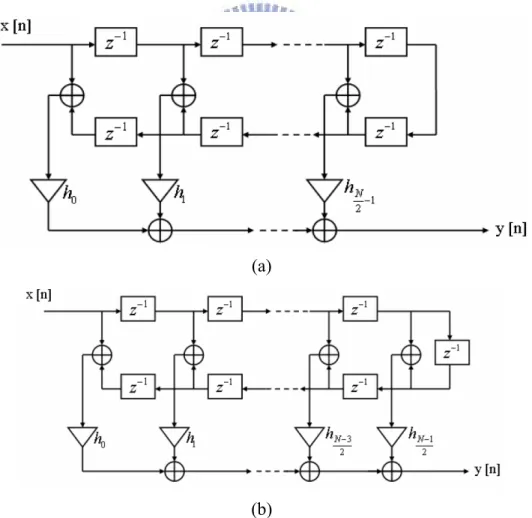
Figure 2 - 8: Linear phase architecture of N-tap FIR filter, (a) when N is even and (b) N is odd.
We can simplify the direct architecture to linear phase architecture. The linear phase architecture of N-taps is shown in Figure 2-8. Due to the advantage of linear phase of FIR filter, the half multipliers can be reduced to lower the complex of this circuit.
2 - 3 CIC (Cascaded Integrator-Comb) Filter
As data converters become faster and faster, the application of narrow-band extraction from wideband sources, and narrow-band construction of wideband signals is becoming more important. These functions require two basic signal processing procedures: decimation and interpolation. And while digital hardware is becoming faster, there is still the need for efficient solutions. Techniques found in [8] work very well in practice, but large rate changes require very narrow band filters. Large rate changes require fast multipliers and very long filters. This can end up being the largest bottleneck in a DSP system.
In [10], an efficient way of performing decimation and interpolation was introduced. Hoginauer devised a flexible, multiplier-free filter suitable for hardware implementation, that can also handle arbitrary and large rate changes. These are known as cascaded integrator-comb filter, or CIC filters for short. An overview can also be found in [9]. An extension of CIC filters has been published in [11], and is briefly mentioned here.
2 - 3 - 1 Building Blocks
The two basic building blocks of a CIC filter are an integrator and a comb. An integrator is simply a single-pole IIR filter with a unity feedback coefficient:
This system is also known as an accumulator. The transfer function for an integrator on the z-plane is
( ) 1 1 1 I H z z− = − . (2.17) Using the Eq. from [12] for a single pole system, we can determine that
| ( ) |2 1 2(1 cos ) j I H eω ω = − , (2.18) [ ( )] tan [1 sin ] 1 cos j I ARG H eω ω ω − = − − , (2.19) , 0 [ ( )] 1 , 0 2 j I undefined grd H eω ω ω = ⎧ ⎪ = ⎨ − ≠ ⎪⎩ . (2.20) The power response is basically a low-pass filter with a -20dB per decade rolloff, but with infinite gain at DC. This is due to the single pole at z = 1; the output can grow without bound for a founded input. In other words, a single integrator by itself is unstable.
Figure 2 - 9: Basic Integrator.
A comb filter running at the high sampling rate, f , for a rate change of R is an s
odd-symmetric FIR filter described by
In this Eq., M is a design parameter and is called the differential delay. M can be any positive integer, but it is usually limited to 1 or 2. The corresponding transfer at
s f
( ) 1 RM C
H z = −z− . (2.22) Again, we can determine that
| ( j ) |2 2(1 cos ) C H eω = − RMω , (2.23) [ ( )] 2 j C RM ARG H eω = − ω , (2.24) [ ( )] 2 j C RM grd H eω = . (2.25) When R = 1 and M = 1, the power response is a high-pass function with 20dB per decade gain. When RM ≠ , then the power response takes on the familiar raised 1 cosine form with RM cycles from 0 to 2π .
When we build a CIC filter, we cascade, or chain output to input, N integrator sections together with N comb sections. This filter would be fine, but we can simplify it by combining it with the rate changer. Using a technique for multirate analysis of LTI systems from [8], we can “push” the comb sections through the rate changer, and have them become
[ ]y n =x n[ ]−x n[ −M]. (2.26) At the slower sampling rate fs
R . We accomplish three things here. First, we have slowed down half of the filter and therefore increased efficiency. Second, we have reduced the number of delay elements needed in the comb sections. Third, and most important, the integrator and comb structure are now independent of the rate change. This means we can design a CIC filter with a programmable rate change and keep the same filtering structure.
Figure 2 - 10: Basic Comb filter.
To summarize, a CIC decimator would have N cascaded integrator stages clocked at f , followed by a rate change by a factor R, followed by N cascaded comb stages s running at fs
R . A CIC interpolator would be N cascaded comb stages running at s f R , followed be a zero-stuffer, followed by N cascaded integrator stages running at f . s
Figure 2 - 11: Three Stage Decimating CIC Filter.
Figure 2 - 12: Three Stage Interpolating CIC Filter.
2 - 3 - 2 Frequency Characteristics
The transfer function for a CIC filter at f is s1 1 0 (1 ) ( ) ( ) ( ) ( ) (1 ) RM N RM N N k N I C N k z H z H z H z z z − − − − = − = = = −
∑
. (2.27) This Eq. shows that even though a CIC has integrators in it, which by themselves have an infinite impulse response, a CIC filter is equivalent to N FIR filters, eachhaving a rectangular impulse response. Since all of the coefficients of these FIR filters are unity, and therefore symmetric, a CIC filter also has a linear phase response and constant group delay.
The magnitude response at the output of the filter can be shown to be
| ( ) | sin sin N Mf H f f R π π = . (2.28)
By using the relation sin x x≈ for small x and some algebra, we can approximate this function for large R as
| ( ) | sin N Mf H f RM Mf π π ≈ , for 0 f 1 M ≤ < . (2.29)
We can notice a few things about the response. One is that the output spectrum has nulls at multiples of f 1
M
= . In addition, the region around the null is where aliasing/imaging occurs. If we define f to be the cutoff of the usable passband, then c the aliasing/imaging regions are at
(i− fc)≤ ≤ +f (i fc), (2.30) for 1 2 f ≤ and 1, 2,..., 2 R i= ⎢ ⎥⎢ ⎥ ⎣ ⎦. If c 2 M
f ≤ , then the maximum of these will occur at the lower edge of the first band, 1− . The system designer must take this into fc
consideration, and adjust R, M, and N as needed.
Another thing we can notice is that the passband attenuation is a function of the number of stages. As a result, while increasing the number of stages improves the imaging/alias rejection, it also increases the passband “droop.” We can also see that the DC gain of the filter is a function of the rate change.
2 - 3 - 3 Bit Growth
For CIC decimators, the gain G at the output of the comb section is ( )N
G= RM . (2.31) Assuming two’s complement arithmetic, we can use this result to calculate the number of bits required for the last comb due to bit growth. If B is the number of in input bits, then the number of output bits, B , is out
Bout =⎡⎢Nlog2RM +Bin⎤⎥. (2.32)
It also turn out that B bits are needed for each integrator and comb stage. The out input needs to be sign extended to B bits, but LSB’s can either be truncated or out
rounded at later stages. The analysis of this is beyond the scope of this tutorial, but is fully described in [10].
For a CIC interpolator, the gain, G, at the ith stage is
2 2 , 1, 2,..., 2 ( ) , 1,..., 2 i N i i N i i N G RM i N N R − − ⎧ = ⎪ = ⎨ = + ⎪⎩ . (2.33) As a result the register width, W , at ith stage is i
Wi =⎡⎢Bin+log2Gi⎤⎥, (2.34)
and
WN =Bin+ − . (2.35) N 1 If M = 1. Rounding or truncation cannot be used in CIC interpolators, except for the result, because the small errors introduced by rounding or truncation can grow without bound in the integrator sections.
It is now worth revisiting the unstable aspect of the integrator stages. It turns out that it is not a problem. For decimators, integrator overflow is not a problem as long as two’s complement math is used and we don’t expect an overall system gain > 1. For interpolators, the comb stages and zero stuffing will prevent integrator overflow.
2 - 3 - 4 Implementation Details
Due to the passband droop, and therefore narrow usable passband, many CIC designs utilize an additional FIR filter at the low sampling rate. This filter will equalize the passband droop and perform a low rate change, usually by a factor of two to eight.
In many CIC designs, the rate change R is programmable. Since the bit growth is a function of the rate change, the filter must be designed to handle both the largest and smallest rate changes. The largest rate change will dictate the total bit width of the stages, and the smallest rate change will determine how many bits need to be kept in the final stage. In many designs, the output stage is followed by a shift register that selects the proper bits for transfer to the final output register. A system designer can use the Eq. for B for a decimator and out W2 N for an interpolator to calculate proper
shift values.
For a CIC decimator, the normalized gain at the output of the last comb is given by 2 ( ) 2 log N RM g N RM = ⎡ ⎤ ⎢ ⎥ . (2.36)
This lies in the interval 1,1 2
⎛ ⎤
⎜ ⎥
⎝ ⎦. Note that when R is a power of two, the gain is unity. This gain can be used to calculate a scale factor, s, to apply to the final shifted output. 2 log2 ( )N N RM s RM ⎡ ⎤ ⎢ ⎥ = . (2.37)
Which lies in the interval
[
1, 2)
. By doing this, the CIC decimation filter can have unity DC gain.2 - 3 - 5 Sharpened CIC Filters
Filter sharpening can be used to improve the response of a CIC filter. This technique applies the same filter several times to an input to improve both passband and stopband characteristics. If H(z) is a symmetric FIR filter, then a sharpened version, ( )HS z , can be expressed as
( ) 2( )[3 2 ( )]
S
H z =H z − H z . (2.38) The magnitude response of a sharpened CIC filter would then be
2 3 sin sin ( ) 3 2 sin sin N N Mf Mf H f f f R R π π π π ⎛ ⎞ ⎛ ⎞ ⎜ ⎟ ⎜ ⎟ = ⎜ ⎟ −⎜ ⎟ ⎜ ⎟ ⎜ ⎟ ⎝ ⎠ ⎝ ⎠ . (2.39)
The interested reader is referred to [11] for more details. Please note that it uses different parameters and implements a CIC filter a bit differently than [10].
Since their inception, CIC filters have become an important building block for DSP systems. They have found a particular niche in digital transmitters and receivers. They are currently used in highly integrated chips from Intersil, Graychip, Analog Devices, as well as other manufacturers and custom designs.
2 - 4 Relative Architecture Survey
We find three relative papers to our design. The first one is “Very Low-Voltage Digital-Audio ΔΣ Modulator with 88-dB Dynamic Range Using Local Switch Bootstrapping.”[1] The second one is “A 2.5-V 14-bit, 180-mW Cascaded ΣΔ ADC for ADSL2+ Application.”[3] The third one is “A Reconfigurable A/D Converter for 4G Wireless Systems.”[22]. They will be introduced as follows.
2 - 4 - 1 Very Low-Voltage Digital-Audio ΔΣ Modulator with 88-dB
Dynamic Range Using Local Switch Bootstrapping
A 1-V 1-mW 14-bit ΔΣ modulator in a standard CMOS 0.35-um technology is resented in this paper. Special attention has been given to device reliability and power consumption in a switched-capacitor implementation. A locally bootstrapped symmetrical switch that avoids gate dielectric overstress is used in order to allow rail-to-rail signal switching. The switch constant overdrive also enhances considerably circuit linearity. Modulator coefficients of a single-loop third-order topology have been optimized for low power. Further reduction in the power consumption is obtained through a modified two-stage opamp. Measurement results show that for and oversampling ratio of 100, the modulator achieves a dynamic range of 88 dB, a peak signal-to-noise ratio of 87 dB and a peak signal-to-noise-plus-distortion ratio of 85 dB in a signal bandwidth of 25 kHz.
Figure 2 - 14: Transistor-level implementation of the bootstrapped switch.
2 - 4 - 2 Cascaded ΣΔ ADC for ADSL2+ Application
This paper presents a sigma-delta analog-to-digital converter for the extended bandwidth asymmetric digital subscriber line application. The core of the ADC is a cascaded 2-1-1 sigma-delta modulator that employs a resonator-based topology in the first stage, three tri-level quantizers, and two different pairs of reference voltages. As shown in the experimental result, for a 2.2-MHz signal bandwidth, the ADC achieves a dynamic range of 86 dB and a peak signal-to-noise and distortion ratio of 78 dB with an oversampling ratio of 16. It is implemented in a 0.25-um CMOS technology, in a 2.8 mm2 active area including decimation filter and reference voltage buffers, and dissipates 180 mW from a 2.5-V power supply.
Figure 2 - 15: Block diagram of RMASH 2-1-11.5b.
2 - 4 - 3 A Reconfigurable A/D Converter for 4G Wireless System
This paper presents a multi-standard reconfigurable Sigma-Delta modulator, which is able to support the predictable standards of fourth generation of mobile communication systems (4G). Furthermore, the proposed architecture halves the number of required analog-to-digital converters in parallel receivers, by processing concurrently two different signals. The major design issues are outlined and operation modes are detailed. A system-level simulation is performed to demonstrate the feasibility of the presented solution. The modulator is implemented into switched-capacitor circuits and device level simulations demonstrate the performance of the converter.Table 2: Modulator Transfer Functions.
Digital filters
Modulator Output
Standard
GSM
H1 H2 H3
Y
Mode 1
- - - U(z)+E1(z) (1-z-1)2Mode 2
z-2 (1-z-1)2 - U(z)z-2+E1(z) (1-z-1)4Mode 3
z-2 - (1-z-1)2 U(z)z-2+E1(z) (1-z-1)2Chapter 3
System Architecture
In this chapter, we introduce the detail architecture of this ADC. The introduction includes which circuit we use, how we make the specification, simulation result of all components and how we simplify the circuit to decrease the cost. Due to the low-voltage architecture, comparing to high-voltage design we have to do some changes.
To confirm the accuracy of the architecture, we do the behavior simulation of the 2nd-order Sigma-Delta modulator by MATLAB. And we also can make the specification of the real circuit by MATLAB. After this simulation, we can design all the components, then using these components to realize a 2nd-order Sigma-Delta modulator.
The sampling-rate has to down sample to twice bandwidth of input signal and filter the noise in high frequency because of the oversampling and noise shaping technique of Sigma-Delta modulator. We use the low pass filter to avoid aliasing also. The input of the digital decimation filter is 1-bit input. And the bit number depends on the ENOB of the output of Sigma-Delta modulator. In this design, the ENOB is 10-/8-bit for each mode. Normally, the digital part of a Sigma-Delta ADC will cost more than half power and half area of the ADC. The most important issue for designing the digital decimation filter is how to reduce the power consumption and area.
3 - 1 Architecture of Sigma-Delta ADC
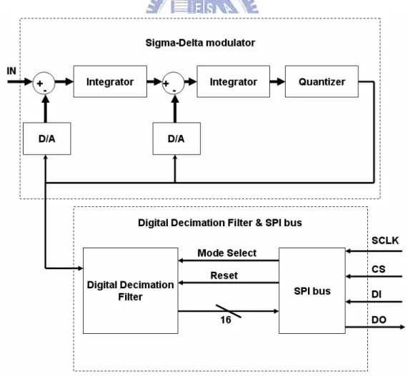
This ADC is composed of Sigma-Delta modulator, decimation filter, SPI bus and other control units. The block diagram of this ADC is shown in Figure 3-1 and Figure 3-2. The first block is Sigma-Delta modulator which can lower the in-band noise by skills of oversampling and noise shaping. And the decimation filter can filter the noise in high frequency and decimate the sampling frequency to twice of input bandwidth. In the end, the ADC output the data by SPI to DSP beyond this ADC. Then the DSP can analyze the date (bio-electric signal or bio-image signal). And all components of this ADC will be introduced in the back chapters. In this design, 2nd-order Sigma-Delta modulator is chosen. Due to the small input bandwidth, we choose high OSR not architecture of high order to reach the same resolution.
Figure 3 - 2: Block diagram of this Sigma-Delta ADC with all necessary IOs.
3 - 2 Behavior Simulation of Sigma-Delta Modulator
Before designing the real circuit, we simulate the function of 2nd-order Sigma-Delta modulator by SIMULINK in MABLAB first.
This ADC is designed for bio-electric signal and bio-image signal both to save the area. So we have to discuss the bandwidth of the two signal to make the sampling frequency. We can see that bandwidth of bio-electric signal is in 1.25 kHz in Figure 3-3. And the bandwidth of bio-image signal is about in 10 kHz.
According to the bandwidth shown up, we make the specification of the ideal 2nd-order Sigma-Delta modulator as Table 3. And we can see that the sampling frequency of the ADC is 640 kHz.
Figure 3 - 3: Bandwidth of bio-electric signals.
Table 3: Specifications of 2nd-order Sigma-Delta modulator
Signal type
Bandwidth OSR Sampling rate
Bio-electric signal 1.25kHz 256Bio-image signal 10kHz 32 640kHz
A block diagram of a 2nd-order Sigma-Delta modulator is shown in Figure 3-4, and we use 1-bit quentizer here. we change the block diagram to signal flow as shown in Figure 3-5, we can calculate the transfer function of X, E and Y (X means the input, Y means the output and E means the quantization error).
The transfer function is shown in below.
2 1 2 1 2 2 1 2 1 2 1 2 2 2 1 2 2 [ ] (1 ) [ ] [ ] ( 1 ) ( 2) 1 ( 1 ) ( 2) 1 Y z a a z z X z E z a b b z b z a b b z b z − − − − − − − = + + − + − + + − + − + . (3. 1)
Figure 3 - 4: Block diagram of a 2nd-order Sigma-Delta modulator.
Figure 3 - 5: Flow diagram of 2nd-order Sigma-Delta modulator. If we let a1 = a2 = b1 = 1 and b2 = 2, then we can simplify Eq. (3.1) as blow: [ ] 2 [ ] (1 1 2) [ ] [ ] [ ] [ ] [ ]
Y z =z X x− + −z− E x =STF z X z +NTF z E z . (3. 2) As upper Eq., we can see that STF is a low-pass filter for input signal, and NTF is a high-pass filter for quantization noise (or white noise). So the operation theorem of Sigma-Delta modulator is keep the signal in input bandwidth, and remove the quantization noise to high frequency from low frequency.
But considering the real situation, the integrator is made by a fully differential opamp, so the output swing will limit to the output swing of fully differential opamp. Especially the first integrator, has the greater effect than the second one. Due to the circuit beyond the second integrator is a 1-bit quantizer which only cares about the output of the second integrator is positive or negative. So the real output of the second
integrator is not so important. We have to adjust the parameter of Eq. (3.2), a1 , a2, b1 and b2 without changing the behavior of the modulator, because of the limit of output swing. We choose a1 = b1 = 0.25, a2=1 and b2=0.5 to make sure that the output swing of the first integrator can be smaller.
As the upper discussing, we make sure the architecture of the 2nd-order Sigma-Delta modulator. Now we discuss the SNDR, ENOB and the output of different stages of the two different modes (bio-electric signal mode and bio-image signal mode).
3 - 2 - 1 Simulation in Bio-electric Signal Mode
Bandwidth of bio-electric signal is in 1.25 kHz. To test the function, we input the sine wave of 400 Hz to simulate.
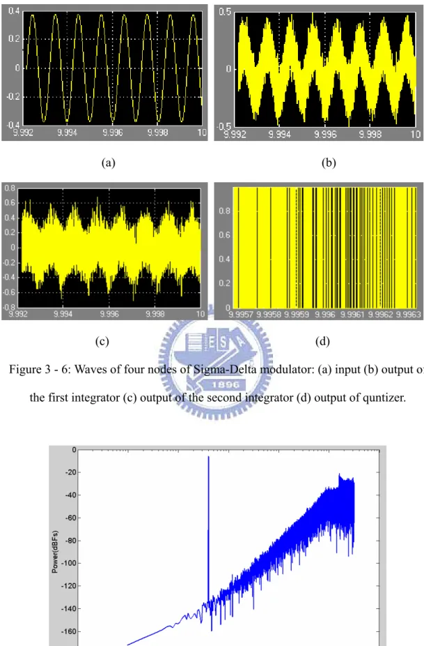
The outputs of four stages is shown in Figure 3-6, when input signal is sine wave of 400 Hz, Vp-p = 0.375 V and 640 kHz sampling frequency.
As shown in Figure 3-6, we can see the output of the Sigma-Delta modulator is a square wave with different width. We change the output to frequency domain by FFT to observe its spectrum which is shown is Figure 3-7. We can get the SNDR is 98.1837 dB, and ENOB is 16-bit in bio-electric signal mode. This spectrum shows that the function of block diagram of modulator is correct. Next we observe the relationship between DR (dynamic range) and SNDR in the same OSR. It’s shown in
(a) (b)
(c) (d)
Figure 3 - 6: Waves of four nodes of Sigma-Delta modulator: (a) input (b) output of the first integrator (c) output of the second integrator (d) output of quntizer.
Figure 3 - 8: SNDR versus input lever in bio-electric signal mode.
3 - 2 - 2 Simulation in Bio-Image Signal Mode
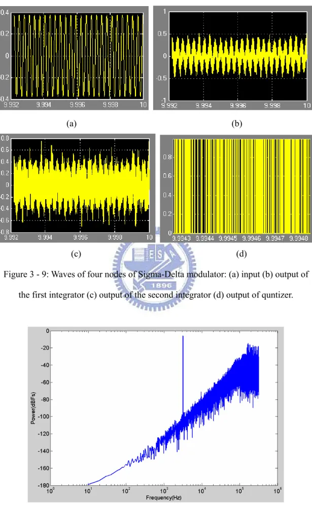
Bandwidth of bio-image signal is in 10 kHz. To test the resolution of this mode, we input the sine wave of 3.2 kHz to simulate.
The outputs of four stages is shown in Figure 3-9, when input signal is sine wave of 3.2 kHz, Vp-p = 0.375 V and 640 kHz sampling frequency.
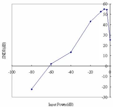
As shown in Figure 3-9, we can see the output of the Sigma-Delta modulator is a square wave with different width. We change the output to frequency domain by FFT to observe its spectrum which is shown is Figure 3-10. We can get the SNDR is 54.7919 dB, and ENOB is 9-bit in bio-image signal mode. Next we observe the relationship between DR (dynamic range) and SNDR in the same OSR. It’s shown in
(a) (b)
(c) (d)
Figure 3 - 9: Waves of four nodes of Sigma-Delta modulator: (a) input (b) output of the first integrator (c) output of the second integrator (d) output of quntizer.
Figure 3 - 11: SNDR versus input level in bio-image signal mode.
As shown above, we can get resolution we need in sampling rate of 640 kHz, no matter the mode we choose is bio-electric signal mode or bio-image signal mode. But that’s the ideal situation; in real case, the resolution will be affected under some non-ideal conditions of real circuit. We will introduce the components of the Sigma-Delta modulator, and how we make the specifications of them to let the resolution under acceptable range.
3 - 3 Architecture and Design of Sigma-Delta Modulator
The 2nd-order Sigma-Delta modulator desired is composed of clock generator, switch for low voltage supply, comparator and opamp. How we make the specifications of them, and the simulation result are introduced as follows.
3 - 3 - 1 Non-overlap Clock Generator
All clock phases of the Sigma-Delta modulator is generated by the clock generator. It’s a key point about if the Sigma-Delta can work correctly. It only needs two inverse
phases of clock when we simulate a ideal modulator. But when we design a non-ideal or real modulator, it needs four phases clock which are non-overlapping to control the modulator. As shown in Figure 3-12, it has a time delay between P1and P1d. It also has a time delay between P2and P2d. The delay of the non-overlapping phases of clock is to avoid charge injection and clock feedthrough.
Figure 3 - 12: Four non-overlap clocks.
Clock generator is composed of nor gates, inverters and same delay cells. As shown in Figure 3-13, the delay cells are composed of some inverters to produce different delay times to control the modulator and make sure the modulator can work properly. P1 and P2 are two inverse phases, and P1d and P2d are their delay phases respectively. And the other four phases clock shown in Figure 3-13, are the inverse phases of P1, P2, P1d and P2d.
Figure 3 - 14: Simulation result of clock generator.
3 - 3 - 2 Bootstrapped Switch
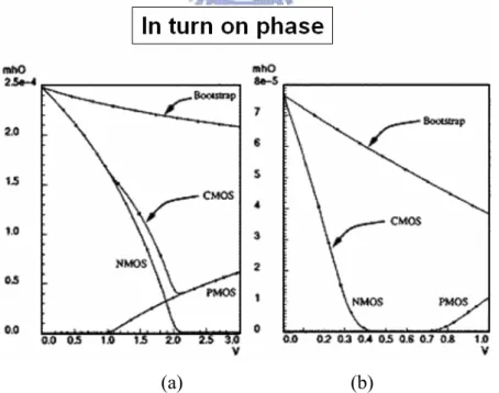
In order to design a low power consumption ADC, we use 1.5 V to be our voltage supply. As shown in Figure 3-15, we can see a problem of that normal mos switch can’t be turned on properly in low voltage supply. Differently, bootstrapped switch can work in low voltage supply properly. And the value of Gon of bootstrapped switch is almost the same when different input voltage is supplied. So in this design, some switches are chosen to be bootstrapped switches to carry the right data.
(a) (b)
Figure 3 - 15: Gon of nmos, pmos and bootstrapped switch versus input voltage when (a) VDD=3V (b) VDD=1V.
Illustration of bootstrapped switch as shown in Figure 3-16, additionally, clk and clkb are two inverse clocks. In clkb phase, the capacitor C will be charged to VDD and the switch SW will be turned off; in clk phase, the switch SW will be turned on and the voltage of gate will be about Vin + VDD, because of charging of C in clkb phase. So the switch SW will make sure to be turn on and work well in clk phase.
Some switches in Sigma-Delta modulator will be bootstrapped switches. When the input signal is always low voltage, the switches used will be nmos switches; in other hand, when the input signal is uncertain, the switches used will be bootstrapped switches.
(a)
(b) (c)
Figure 3 - 16: (a) circuit of bootstrapped switch (b) during clkb phase (c) during clk phase.
In this design, the circuit of bootstrapped switch is shown in Figure 3-17 [1]. MNT5 is added to prevent the gate-drain voltage of MN5 from exceeding VDD while it is off. MP2 and MP4 must be tied to the highest potential, node B. Transistor MN6S triggers MP2 on at the beginning of while transistor MN6 keeps it on as the voltage on node A rises to the input voltage Vin. Gate connections of transistors MN1 and MN6 allow them to be turned on similar to the main switch MNSW.
The simulation result of bootstrapped switch is shown in Figure 3-18. In this case, VDD = 1.5 V and input is sine wave with 0 ~ 1.5 V voltage. No matter what the input voltage is, the output is the same as input voltage in Φ phase. 1
Figure 3 - 17: Transistor level implementation of the bootstrapped switch.
3 - 3 - 3 Comparator
The SNDR of comparator with offset voltage = 0 V and offset voltage = 15 mV versus input level is shown in Figure 3-19. We can see that when offset voltage is 15mV, the SNDR value is almost the same as the ideal situation. The specification of Sigma-Delta modulator will not be affected by the offset and hysteresis of comparator, because those non-ideal signal will be shaped to high frequency as the quantization noise. Here, we set the offset of comparator to be ± 15mV.
(a) (b)
Figure 3 - 19: The SNDR versus input level (a) in bio-electric mode (b) in bio-image mode when offset voltage is 0V and 15mV.
The circuit of comparator is shown in Figure 3-20. It’s a usual comparator circuit. When V(in+) > V(in-), the output Y will be high level (V(Y)=VDD=1.5V); in the other hand, when V(in+) < V(in-), the output Y will be low level (V(Y)=VSS=0V). Additionally, the switch between out+ and out- is bootstrapped switch.
0.735, 1.5, 0, 0.765, 0, 0.8, 0.5, 0.765, 0.735, 1.2, 0.3, 0.77, 0.73)V, V(in-) = 0.75V; V(in+) = (1.015, 0.9, 1.03, 0.8, 0.985, 1.2, 0.95, 1.1, 0, 1.015, 0, 1.5, 0.985,1.5)V, V(in-) = 1V; V(in+) = (0.52, 0.4, 0.6, 0.47, 0.6, 0, 0.515, 0, 1.5, 0.485, 1.5, 0.4, 0.52, 0.48)V, V(in-) = 0. 5V. And simulation results of 5 corners are shown in Figure 3-21, additionally, the waves on the top of every figure are the values of (V(in+)-V(in-)) in every simulation. The simulation results tell us that the offset of the comparator is 15mV, and its current consumption is 1.99 uA.
(a)
(b)
(c)
Figure 3 - 21: Simulation results of testing of the comparator. (a) first pattern (b) second pattern (c) third pattern.
3 - 3 - 4 Operation Amplifier
When we design a operation amplifier (opamp), we have to consider a lot of specifications, as power consumption, output swing, slew rate and DC gain etc.
First, we discuss the issue of output swing by simulink. The biggest output will happen when the input is between 0.75~-0.75 V. In this situation, the output of the first integrator will be between 0.844~-0.844 V. It means that output swing of the opamp is at least 1.688 V (0.844~-0.844 V). The output of the first integrator which is simulated by simulink is shown in Figure 3-22. Due to the circuit beyond the output of the second integrator is a comparator, the output swing of the second integrator is not so important. It only has to consider if the output of the second integrator is bigger or smaller than 0.
Figure 3 - 22: the output of the first integrator which is simulated by simulink.
Next we consider the issue of slew rate. The variation of the output of opamp in half of clock cycle (1/(640000*2)s) will not be over 1.5 V. And we hope the output can rise to 1.5 V in 1/10 of clock cycle, so we get
1.5 9.6( / ) 1 1 1 * * 640000 2 5 V us = . (3. 3)
In this design, we set the slew rate of the opamp has to be bigger than 9.6 V/us. Then we talk about the dc gain. A normal integrator is shown in Figure 3-23. In this case, switches S1 and S3 are controlled by the same phase clock1; in the other hand, switches S2 and S4 are controlled by the same phase clock2 which is non-overlapping with clock1.
Figure 3 - 23: Inverse integrator with single end.
We can get the function of this integrator shown in Figure 3-23:
1 1 1 1 2 1 1 1 2 1 2 2 1 2 1 / [ ] / [ ] 1 1 (1 ) 1 / Av C Av C C C Vout z z z Av C C Vin z C z C z Av C C Av − − − − + + = ≅ − − − + + . (3. 4)
There is error coefficient e C C1/ 2
Av
= in Eq. (3.4). a1 and a2 are 0.25 and 1 respective,
so the biggest C1/C2 is 1. The SNDR with infinite gain and gain of 73.3dB versus input level is shown in Figure 3-24. When dc gain of opamp is 73.3dB, the error coefficient e will be 2.16×10⁻⁴. In Figure 3-24, we can see that the SNDR won’t be worse when the dc gain of opamp is 73.3dB.
(a) (b)
Figure 3 - 24: The SNDR with infinite dc gain and gain of 73.3 db versus input level. (a) in bio-electric signal mode (b) in bio-image signal mode.
Considering the low voltage supply, we choose a circuit of opamp which applies to low voltage supply. The circuit of the opamp is shown in Figure 3-25. It is a two stage opamp with some variations in the load of differential pair to let the opamp suit for low voltage supply. And we add two compensated capacitors to compensate the bandwidth and phase margin of this opamp.
The frequency response of the opamp is shown in Figure 3-26. When temperature is 25 C° and VDD is 1.5 V, the DC gain of the opamp is 81 dB, unit-gain bandwidth is 11.5 MHz, current consumption is 320.5 uA, phase margin is 65D and the gain is
above 60 dB between 0 Hz ~ 10 kHz.
We simulate the opamp in voltage supply of 1.5V±10% (1.35 V ~ 1.65 V) and temperature of 0DC~ 90DC to make sure that the opamp can work well in different situations. The simulation result is shown in Figure 3-27, it has DC gain 73.3 dB, unit-gain bandwidth 11.5 MHz, phase margin is 65D and the gain is above 60 dB
between 0 Hz ~ 10 kHz.
Figure 3 - 27: Frequency responses of opamp when voltage supply is 1.5V±10% (1.35 V ~ 1.65 V) and temperature is 0DC ~ 90DC.
To test the output swing and slew rate of the opamp, we connect the circuit as shown in Figure 3-28. In this case, R1=100kΩ , R2=112.6k Ω , Vid=(Vi+)-(Vi-) and Vout=(Vout+)-(Vout-). Let Vid be a sine wave with 1.5 V and 20 kHz to test if the output swing is sine wave with 1.688 V. Figure 3-29 shown us that output swing of the opamp has at least 1.688 V. And the output wave at the beginning is not stable because the operation of CMFB is still on the unstable state. We change the Vid to a square wave to test the slew rate of the opamp. The result is shown in Figure 3-30. The slew rate is 10.2 V/us. The detailed specifications of opamp and comparator are shown in Table 4.
Figure 3 - 28: Testing circuit.
Figure 3 - 29: Output of testing circuit when Vid is a 20 kHz sine wave with 1.5 V Vp-p.
Table 4: The specifications of opamp and comparator. Voltage supply 1.5V±10%
DC gain 81dB
Slew Rate 10.2V/us Output swing 1.688V unity gain bandwidth 11.5MHz
Temperature 0°C~ 90°C Current Consumption 320.5uA
Opamp
Phase Margin 65∘
Offset ±15mV
Comparator
Current Consumption 1.99uA
3 - 4 2
nd-Order Sigma-Delta Modulator
We realize the 2nd-order Sigma-Delta modulator by the components introduced above. The simulation result will be discussed as follows.
As the architecture shown in Figure 3-4 by simulink, we can design the Sigma-Delta modulator. The whole circuit of the modulator is shown in Figure 3-31. Due to using the low voltage supply, some switches are bootstrapped switches introduced above. To avoid the area of the chip will become bigger, we use two common-mode voltage in this design, here, one is Vcmout, the other one is Vcmin. In the input of the second integrator we use Vcmout which is equal to VDD/2. And We use Vcmin which is equal to 0 V to implement other ground. So the switches connect with Vcmin can be nmos switch to transit the signal. The use of Vcmout and Vcmin is introduced in [1] particularly.
Figure 3 - 31: Circuit of the 2nd-order Sigma-Delta modulator.
Inverse integrator is used in this design. To eliminate the offset, 1/f noise and finite dc gain, the CDS (Correlated Double Sampling) technique [6] as shown in
Figure 3-32 is used. The CDS technique is used widely to realize the S/H and
integrator of high resolution.
Adding a fitting C in the integrator is shown in ds Figure 3-32. When in
Φ
1phase, the C stores the offset voltage of opamp; when in ds
Φ
2 phase the offsetvoltage of opamp will be eliminated by the charge stored in C at last half cycle. ds
We can express that operation as Eq. (3.5).
1 2