行政院國家科學委員會專題研究計畫 期中進度報告
子計畫二:以正交分頻多工為基礎之多模式基頻收發器研製
(2/3)
計畫類別: 整合型計畫 計畫編號: NSC92-2220-E-009-019- 執行期間: 92 年 08 月 01 日至 93 年 07 月 31 日 執行單位: 國立交通大學電子工程學系 計畫主持人: 李鎮宜 報告類型: 完整報告 報告附件: 出席國際會議研究心得報告及發表論文 處理方式: 本計畫可公開查詢中 華 民 國 93 年 6 月 1 日
行政院國家科學委員會補助專題研究計畫
□ 成 果 報 告 ■ 期中進度報告用於軟體無線電基頻處理之系統晶片設計技術
子計劃二:以正交分頻多工為基礎之多模式基頻收發器研製(1/3)
計畫類別:□ 個別型計畫 ■ 整合型計畫
計畫編號:NSC 91-2218-E-009-010
執行期間:
92 年 11 月 1 日 至 93 年 7 月 31 日
計畫主持人:李鎮宜
計畫參與人員: 林建青、陳黎峰、許騰仁、施彥旭、俞壹馨、管成偉、曾
逸晨、劉子明
成果報告類型(依經費核定清單規定繳交):□ 精簡報告
■
完整報告
處理方式:除產學合作研究計畫、提升產業技術及人才培育研究計畫列管
計畫及下列情形者外,得立即公開查詢
■涉及專利或其他智慧財產權,□一年■二年後可公開查詢
執行單位:國立交通大學電子工程學系
中 華 民 國 92 年 5 月 29 日
中文摘要 此期中報告,主要針對數位視訊廣播系統(DVB-T)的正交分頻多工基頻系 統,進行關鍵技術的研究,包含同步子系統的演算法,高點數 FFT 處理器的設 計,和FEC 中的 Viterbi 解碼器設計。為有效提供同步演算法的系統效能分析, 系統模擬平台的建立頗為重要,因此報告中包含三部份,分別為DVB-T 系統模 擬平台的建構和開發(包含同步、解調變演算法)、高點數 FFT 處理器的設計和前 置錯誤更正解碼器(RS + Viterbi)設計。 關鍵字:數位視訊系統、正交分頻多工、同步演算法、FFT 處理器、前置錯誤更 正解碼器、系統模擬平台 Abstract:
This report describes the project progress in developing core technologies for OFDM-based digital video broadcasting (DVB) system. The research tasks include the following: synchronization algorithm, high-point FFT processor design, and Viterbi decoder used in FEC processor. There are 3 parts in this report, DVB-T simulation platform (including synchronization, demodulation algorithms), high-point FFT processor, and FEC (RS+Viterbi) decoder design.
Keywords: DVB-T System, OFDM, Synchronization Algorithm, FFT processor, Viterbi Decoder, RS decoder, System Simulation Platform.
Part I: DVB-T Baseband System Simulation Platform
AbstractThis baseband DVB-T (Digital Video Broadcasting – Terrestrial [1]) simulation platform is constructed in Matlab platform. It includes transmitter side, channel and receiver side models. All function models are designed by team partners except base functions (AWGN model, FFT operation, convolution polynomial…etc,.) which were built in Matlab library. This platform is a configurable (programmable) platform, which we can add, remove or change function or algorithm models in system organization. All function blocks can be enabled or bypassed in simulation stage, thus we can observe performance budget of each block in several constraints we needed. In this platform, we have already included and completed channel coding blocks, OFDM modulation/demodulation, channel models (Ricean, Rayleigh channel model), timing synchronization, frequency synchronization and equalization algorithms.
1. Introduction
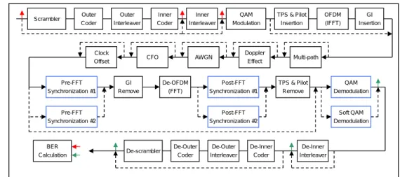
The function blocks in this DVB-T simulation platform were developed by two subgroups, FEC group and modem/synchronization group and have been integrated. All building blocks are shown below:
Figure 1: DVB-T system level block diagram
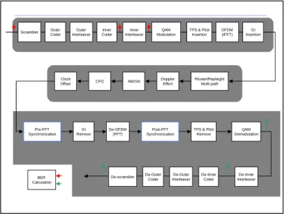
In this building block diagram, all other blocks have been designed, verified in algorithm level in simulation platform [2][3]. In the transmitter side, the FEC part includes Scrambler, Reed-Solomon code (Outer coder), Outer interleaver, Puncturing Convolutional code (Inner coder) and Inner interleaver. The OFDM part includes Mapper, Frame adaptation (pilots & TPS insertion), OFDM operation and Guard interval insertion. In receiver side, the reverse functions are one by one mapping to transmitter side functions. And there are two synchronization system (timing and frequency synchronization system) and equalization algorithm integrated into receiver side to compensate Channel effects.
Post-FFT Synchronization De-Inner Interleaver De-Outer Interleaver De-Outer Coder De-Inner Coder QAM Demodulation TPS & Pilot Remove De-OFDM (FFT) GI Remove De-scrambler Pre-FFT Synchronization BER Calculation Inner Interleaver Outer Interleaver Outer Coder Inner Coder QAM Modulation TPS & Pilot Insertion OFDM (IFFT) GI Insertion Scrambler Clock
Offset CFO AWGN
Ricean/Rayleight Multi-path Doppler
2. Configurable platform
In this section, we will describe the proposed configurable platform, which is constructed based on DVB-T standard and modified by the proposed idea in detail (Figure 2).
Figure 2: DVB-T Configurable platform
In our proposed platform, we are including two multi-path channel models [1], AWGN model, Carrier Frequency Offset, Sampling Clock Offset and Doppler effect [4]. They can be added or bypassed in simulation iteration. Thus we can build any type of channel environment we needed in simulation time. For example, using AWGN, Multi-path, CFO, Sampling Clock Offset and skipping Doppler effect to simulate in-door channel model, and so on. Also, we can turn off the FEC blocks for performance estimation for OFDM blocks or turn off the OFDM blocks for performance estimation for FEC blocks. For the synchronization algorithm surveying, we can change post-FFT, pre-FFT synchronization blocks to verify developing algorithms, and check the simulation results quickly and easily.
In the channel model, we provide several models: Multi-path, Fixed reception, Ricean fading, Portable reception, Rayleigh fading, Doppler Effect and AWGN. These two multi-path channel models are referred to DVB-T standard and the equations are shown below, and parameters also come from DVB-T standard:
∑
∑
− = − − + = N i i N i i j ie x t t x t y i 0 2 1 0 () ( ) ) ( ρ τ ρ ρ θ (1)∑
∑
= = − − = = N i N i i i j ie x t k k t y i 1 1 2 1 ), ( ) ( ρ τ ρ θ (2)where
ρ
i is attenuation of the i’th path,τ
i is the relative delay of the i’th path,θ
i isthe phase shift from scattering of the i’th path. The Doppler effect channel model is drawn in Fig. 3. We have initially assumed a channel with a known and fixed number of paths P, a Doppler frequency fd(k), attenuation ρ(0)ejθ(0), and delay τ(0).
Post-FFT Synchronization #1 Inner Interleaver Outer Interleaver Outer Coder Inner Coder QAM Modulation TPS & Pilot Insertion OFDM (IFFT) GI Insertion Scrambler De-Inner Interleaver De-Outer Interleaver De-Outer Coder De-Inner Coder QAM Demodulation TPS & Pilot Remove De-OFDM (FFT) GI Remove De-scrambler Pre-FFT Synchronization #1 Soft QAM Demodulation Doppler Effect Clock
Offset CFO AWGN
Post-FFT Synchronization #2 Pre-FFT Synchronization #2 BER Calculation Multi-path
Figure 3: Doppler Effect model
Since each path has its own Doppler frequency, how to decide the statistical distribution for fd is important. There are two common Doppler frequency PDFs,
uniform and classical. Obviously, uniform case uses uniform distribution, and classical case uses Jakes’ Doppler spectrum. The PDF of Jakes’ Doppler spectrum is derived as below.
(3)
After transformation of random variable, we can obtain each fd by the following
equation. The type of Doppler spread affects the performance very much even if we choose the same spectrum (uniform or Jakes’). Because each path gets different fd in
each simulation case, the amount of the lost orthogonality will be not the same. Therefore, we should fix each fd in each simulation and comparison.
(4)
In the pre-FFT synchronization block, there are some functions integrated in it (in time domain). They are frame bound detection, symbol synchronization[5], time domain fraction part Auto-Frequency Controller and guard interval remover. We can modify or improve any one of them to generate another one pre-FFT synchronization block, or re-design whole pre-FFT synchronization functions for challenging new coming channel models, such like Doppler effect.
There are several functions block included in the post-FFT synchronization (in frequency domain). They are sampling clock tracking, fine symbol synchronization scheme, integral part Auto-Frequency Controller, frequency tracking scheme, and channel equalizer. We can modify any one of them to improve overall post-FFT synchronization or create another one post-FFT synchronization block.
The BER calculation block(s) can evaluate block performance by comparing the input/output of inverse functions between transmitter and receiver, such like QAM
τ(0) Σ τ(1) τ(P-1) ej2πfd(0)t ej2πfd(1)t ej2πfd(P-1)t ρ(0)ejθ(0) ρ(1) ejθ(1) ρ(P-1)ejθ(P-1) • • • ej2πΔf t n(t)
Doppler CFO AWGN
Delay Attenuation max
))
1
(
2
cos(
d drand
f
f
=
π
⋅
⋅
2 max max 1 1 ) ( − ⋅ ⋅ = d d d d f f f f p π max d df
f
<
modulation input/QAM demodulation output or Inner Encoder input/Viterbi Decoder output. Thus we can estimate performance block by block or for whole system. In the same time, we have reserved output data of each block in simulation time, and then we can compare, check data or system behavior in detail. In other words, we have designed several data comparing or data presenting methods for evaluating simulation results.
3. Receiver blocks structure
The following figures are the detailed block diagram of current version receiver. Figure 4 is the overview of receiver block diagram, and Figure 5 is the inner receiver block diagram (i.e.: demodulation, and synchronization).
Figure 4: receiver block diagram
The data flow is inverse flow of transmitter. All function blocks are reverse function to transmitter function with one to one mapping. The system level simulation is running for overall performance, and the block performance is evaluating for performance budget.
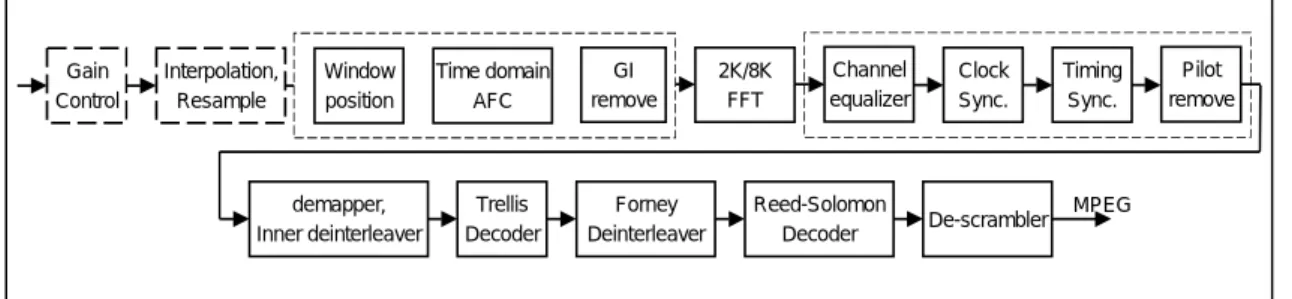
Figure 5: inner receiver block diagram A. Timing Synchronization Algorithms
The timing synchronization system is separated into two parts, Acquisition mode and Tracking mode [6][7], shown in Figure 6. The GI/Mode decision, Coarse Symbol synchronization and SP mode detection block are acquisition mode. These blocks were working in initialization stage only. The GI/Mode decision was using for estimating the operation mode and guard interval length; the coarse OFDM symbol bound decision was performed in Coarse Symbol synchronization. The Scattered Pilot
demapper, Inner deinterleaver MPEG Trellis Decoder Forney Deinterleaver Reed-Solomon Decoder De-scrambler 2K/8K FFT Pilot remove Timing Sync. Clock Sync. Interpolation, Resample Channel equalizer Window position Gain Control Time domain AFC GI remove
GI, mode decision SynchronizationCoarse Symbol WindowFFT
Pre-FFT AFC Carrier Frequency Compensator FFT Post-FFT AFC Sampling Frequency Tracking SP Mode Detection Carrier Frequency Tracking Fine Symbol Synchronization Equalizer Δffr Δfint Δftracking ADC Interpolator/ Decimation
sequence checking is activated in SP mode Detection.
The other three functional blocks in tracking mode are Interpolator, Sampling Frequency Tracking and Fine Symbol Synchronization. The fine-tune process of symbol bound decision is working in Fine Symbol Synchronization. To compensate sample frequency offset, the Sample Frequency Tracking estimates the sampling offset, and then controls the Interpolator/Decimation to resample received data.
Figure 6: Timing synchronization system A.1 Coarse Symbol Synchronization [8]
Based on the previous semester report, several algorithms are analyzed. We choose the first algorithm - maximum correlation, which is simplest and low-cost. That’s because the true design goal of coarse symbol synchronization is not to achieve the highest possible accuracy, but to meet the requirements of following algorithms such as AFC and clock recovery circuit with a minimum implementation cost and fastest process time. Furthermore, considering the architecture of guard interval mode decision block, maximum correlation method has the advantage of combination. We can combine these two blocks if we use maximum correlation method. This algorithm is tolerable enough to large frequency offset and potentially large sampling clock frequency deviations during acquisition, which is shown below.
(5)
In strong multi-path channel, we must take fewer into calculation for avoiding ISI. This method can resist CFO, so the performance is acceptable. In order to switch to guard interval mode decision block, we have to let initial GI be 1/32, that is Ng=64. Then we can obtain mode and guard interval by estimating the period of local maximum.
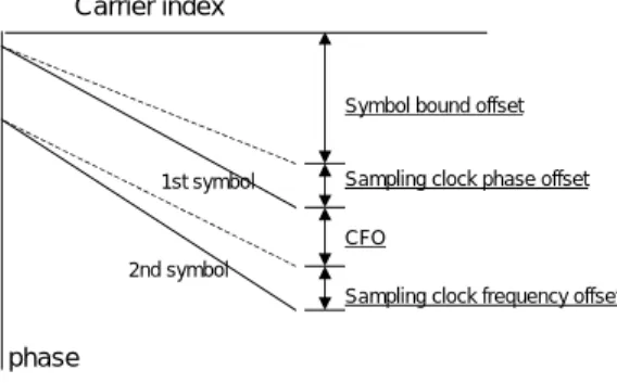
A.2 Sampling Clock Tracking [14]
Figure 7 shows the frequency domain phase rotation occurred between two consecutive received OFDM symbols due to synchronization error. The magnitude of phase rotation due to symbol timing offset is proportional to sub-carrier index. The effect of sampling clock phase offset is similar to the effect of symbol timing offset. In the 2nd symbol, the effect of CFO is constant phase error, and the effect of sampling clock frequency offset is linear phase error. That is a very good property for
FFT ADC Interpolator/ Decimation Fine Symbol Synchronization FFT Window Sampling Frequency Tracking SP Mode Detection Coarse Symbol Synchronization GI, mode decision
∑
− = − ⋅ − − = 1 0 *( ) ) ( max arg Ng i k est r k i r k i N Ksampling clock synchronization. The algorithm is as below.
(6)
(7)
Where C(1|2) denotes 1 for left half of continual pilot index and 2 for right half of continual pilot index.
Figure 7: Phase rotation
The main concept is to calculate the phase difference between left half and right half and normalize it. Nevertheless, the variance of estimation value is also large; a tracking scheme is needed drawn as below.
Figure 8: Timing Recovery Loop
The proposed tracking loop contains one-shot error estimator described as above, loop filter, timing processor, ideal interpolator, and decimator. The loop filter is a so-called “PI loop filter”, which is a simple one-order loop filter including proportional part (KP) and integral part (KI).
(8)
The output of error estimator is sent to PI loop filter. For small system delay, we can let (KI-KP) << KP << 1, so that the steady-state tracking error standard deviation
will be very small.
(9)
2nd symbol 1st symbol
Symbol bound offset
Sampling clock phase offset
CFO
Sampling clock frequency offset
Carrier index phase
(
)
(
l l)
K N Ng 2, 1, ^ 2 / 1 / 1 2 1 ϕ ϕ π ζ ⋅ ⋅ − + = ⋅ =∑
∈ (1|2) − * , 1 , , 2 | 1 C k k l k l l Arg z z ϕ 1 11
)
(
− −−
+
=
Z
Z
K
K
z
F
P I(
/
2
(
)
)
)
'
(
e
K
Pσ
e
σ
=
⋅
Ideal Interpolator FFT Sampling Clock Tracking Timing Processor PI Loop Filter Decimator μk mkThe close-loop tracking time constant is approximately given by
(10)
So there is a tradeoff between performance degradation and tracking convergence speed. After simulation, the proper parameter value of KP and KI are
both 1/64.
A.3 Fine Symbol Synchronization [9][10]
There are two kinds of fine symbol synchronization. One is phase estimation of the scattered pilots, and the other is channel impulse response estimation by IFFT. First method gets delayed symbol boundary in long-path channel but is easily implemented, and second method costs very much (IFFT) but has accurate result even in bad Rayleigh channel. In fact, the BER performance between these two methods is relative small because the difference between an exact boundary and a small delayed boundary is phase rotation of sub-carriers in frequency domain, which can be solved by equalizer. The goal of fine symbol synchronization is to prevent boundary drift caused by residual sampling clock offset. Therefore, the estimation consistency of symbol boundary is more important than accuracy of estimated symbol boundary. Considering above viewpoints as well as hardware cost, we choose first method to simulate. On the other hand, since the equalizer buffers 3 symbols, the impact of window position on the effective channel must be kept in mind. While fine symbol synchronization adjusts the symbol boundary, the estimated channel response has to add sub-carrier phase rotation effect.
B. Frequency Synchronization Algorithms
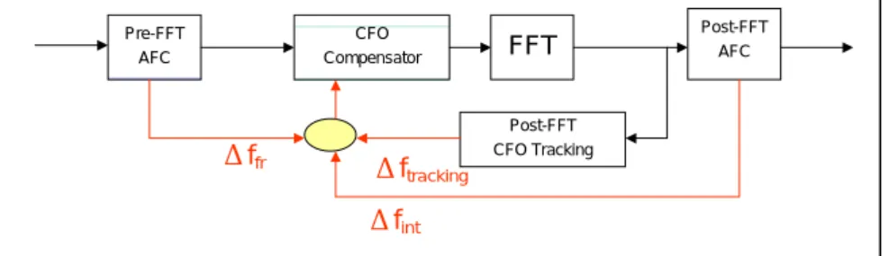
The proposed integrated Automatic Frequency controller (AFC) scheme is mainly composed of estimation part and tracking part. Pre-FFT AFC is estimating the fraction part of Carry Frequency Offset (CFO), Post-FFT AFC is estimating the integral part of CFO, and the Post-FFT CFO Tracking tracks the residual carrier frequency offset respectively. This AFC scheme can estimate the widely range of CFO, 32 sub-carrier spaces, and the residual carrier frequency offset is less than 1/1000 sub-carrier space
Figure 9: Frequency synchronization system
CFO Compensator FFT Pre-FFT AFC Post-FFT AFC Post-FFT CFO Tracking Δffr Δf tracking Δfint P loop
K
T
≈
1
/
B.1 Pre-FFT AFC
In time domain, carrier frequency offset induces linear phase error. So we use this property to propose the algorithm for pre-FFT AFC. The pre-FFT AFC algorithm uses guard-interval (GI), the cyclic prefix data to estimate fraction part of CFO. DVB-T standard defines GI inserted between effective symbols in time domain to avoid inter-symbol interference in multi-path condition [11]. Because GI is copied from the rare part of the following symbol, the phase error between GI and the rare part of the following symbol should be zero. However, if carrier frequency offset occurs, the phase error between GI and the rare part of the following symbol is not zero and in proportional to the fractional part of carrier frequency offset. So this algorithm estimates the fractional part of carrier frequency offset Δffr by calculating
the phase error between GI and the following symbol, and can be expressed as
(11)
where Ng is the length of GI. y is the received symbol in time domain. N is the length of FFT size. And i is the symbol index. This algorithm is unaffected by the integer part of carrier frequency offset and the estimation range is from -0.5~+0.5 because it uses GI and effective symbols in time domain. Besides, DVB-T standard defines an outdoor Rayleigh fading channel [11]. In this channel model, the second latest delay path’s delay time is 3.324866μs. Because the element symbol period in 8mhz channel is equal to 7/64μs, the second latest delay path locates between the 30th symbol and the 31st symbol of GI. In order to avoid the effect of muti-path in GI, we choose n=31. That is to say, we must skip the first 31 symbols of GI when calculating the fractional part of carrier frequency offset. Compare with the algorithm proposed by Beek etc. [12], the proposed algorithm achieves 1.7dB better in BER performance by simulation.
B.2 Post-FFT AFC
From previous section, we can know that carrier frequency offset will shift the positions of sub-carriers in frequency domain, and the shift amount is equal to the value of carrier frequency offset. With this property, post-FFT AFC can estimate the integer part of carrier frequency offset in frequency domain by using continual pilots. Continual pilots are defined by DVB-T standard, and their amplitude and position are fixed on all symbols in frequency domain [11]. Besides, they are transmitted at “boosted” power level so their average power is greater than that of data. So in the proposed algorithm, we estimate the position shift of continual pilots due to carrier frequency offset. In the first step, the proposed algorithm calculates the correlation between two continual pilots with the same sub-carrier index for two successive symbols in frequency domain based on shifting the pilot positions, and can be
] ) ( ) ( [ 2 1 1 *
∑
+ = ⋅ − = ∆ Ng n i fr Arg y i N y i fπ
expressed as
(12)
where Cm means the correlation value and Pm means the positions of continual pilots based on the shift value m, respectively. Y means the received sub-carrier in frequency domain. k means the index of sub-carrier in frequency domain. And j means the symbol index in frequency domain.
In the second step, the integer part of carrier frequency offset Δfint is estimated
by detecting the offset position m where the correlation value Cm is maximized as
(13)
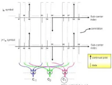
Figure 10 shows the received signal according to the sub-carrier in frequency domain when carrier frequency offset is 1 in DVB-T 2k mode. Therefore, the positions of continual pilots should be 0, 48, 54, 87…. Accordingly, if the maximum value of Cm is obtained from sub-carriers 1, 49, 55, 88…, the estimated integer part of carrier frequency offset is 1, because the position of maximum correlation is achieved one sub-carrier position away from the original continual pilots under noise free conditions.
Figure 10: Received signal according to the sub-carrier.
DVB-T standard defines 45 continual pilots in 2k mode and 177 continual pilots in 8k mode, respectively [11]. Considering low power issue, it is not necessary to use all of the continual pilots when calculating the integer part of carrier frequency offset. By simulation we can choose only 12 of the 45 continual pilots in 2k mode to estimate the integer part of carrier frequency offset correctly. Compare with the algorithm proposed by Han, Seo, and Kim in 2001 [13], the proposed algorithm can save about 3/4 computational quantity.
∑
= − ⋅ = m P k k j k j m Y Y C * , 1 , m mC
f
int=
max
∆
B.3 Carrier frequency offset tracking [14]
The existence of Doppler effect in mobile channel may make the value of carrier frequency offset drift with time. In order to avoid the performance degradation induced by Doppler effect, tracking of carrier frequency offset is necessary. We divide the proposed carrier frequency offset tracking scheme into two stages. In the first stage, continual pilots are used for estimating the value of residual carrier frequency offset. In the second stage, a proportional integral loop filter is used for converging the residual carrier frequency offset value calculated by previous stage. The block diagrams of carrier frequency offset tracking loop are shown in Figure 11.
Figure 11: Block diagrams of carrier frequency offset tracking loop.
When residual carrier frequency offset exists, it will introduce phase error in frequency domain, and can be expressed as
(14)
where z is the received continual pilot when residual carrier frequency offset exists. a is the original continual pilot. ∆f’F is the residual carrier frequency offset. l is
the symbol index and k is the sub-carrier index in frequency domain, respectively. Ns is the length of symbol and Ng is the length of GI in time domain, respectively. T is the element symbol period in time domain. And Φ is the phase of fading channel. If the channel is a slowly fading channel ( ), we can use the rotated phase error between two adjacent symbols to estimate the residual carrier frequency offset, and can be expressed as
(15)
where M means the number of continual pilots. After the first stage calculates the residual carrier frequency offset Δf’F , we send Δf’F into a proportional integral
loop filter. The block diagrams of the loop filter are shown in Figure 12.
) ( ) (k H1 k l H l ≈φ− φ ) ( ) ( ' 2 ) ( ) ( ) (k angle zl,k angle al,k fF lNs Ng T lH k l π φ ϕ = − = ∆ + + T N f k k k l l F s l( )=ϕ ( )−ϕ−1( )=2π∆ ' θ TM N k f s C C s s l F M
π
θ
2 ) ( 1 ' =∑
= ∆Figure 12: Block diagrams of loop filter.
By choosing of Kp and Ki, we can get different convergence speed and tracking error. Detail simulations of Kp and Ki will be introduced in later section.
C. Equalization algorithm
We have designed and analyzed the performance of three types of equalizer; one of them is our proposed equalization algorithm, 2-D filtering non-causal equalizer. It’s workable for DVB-T baseband system under mobile environment. Also, it’s satisfied for in-door channel and terrestrial broadcasting environment.
Channel equalizer is placed after the FFT block in most OFDM systems. Based on the benefit of OFDM properties, pre-defined pilots can be extracted at the pilot locations at the receiver side. That is, for signals X(f) with the pilot inserted at the transmitter side, the IFFT operation makes the transmitted signals x(t) equal to:
(16) Because of multi-path effects, y(t) received at the receiver side is:
(17) Where h(t) is the channel impulse response.
After y(t) flows through an FFT processor at the receiver side we got
(18) So if there are no AWGN effects, then
(19) Where H(f) is the channel frequency response (CFR)
And we can calculate H(f) by
(20) If we known what X(f) is, and X(f) is known at the pilot location, we can know
)} ( { ) (t IFFT X f x = ) ( * ) ( ) (t x t h t y = )} ( { ) (f FT y t Y = ) ( ) ( ) (f X f H f Y = × ) ( / ) ( ) (f Y f X f H =
H(f) at the pilot locations. In addition to multi-path effects, Doppler effects also occur in the transmitting environment. Doppler effects cause the multi-path effect time-invariant. So to estimate the time-invariant channel frequency response more accurately, time domain consideration is also an important issue. And for the time-domain issue, we construct the following 4 types of equalizers.
Based on the DVB-T standard, the performance of channel equalization scheme is depended on the pilot collection strategy and recovering method for channel frequency response. To compensate the time-variant channel effect, Doppler effect, the 2-D pilot collection strategies or similar methods have been accepted. Also, the CFR approximating method or similar CFR calculation formulations were discussed in this research field.
C.1 Simple 1-D equalizer
Due to the Doppler effects, the channel frequency response seen at each OFDM symbol might be different. Therefore, by using pilots at different OFDM symbol might not suit the OFDM symbol currently received. And this simple 1-D equalizer extracts the channel frequency response at all the pilot locations in one OFDM symbol received. Using these collected CFR information, we do the interpolation in frequency domain and obtain the complete set of CFR as Figure 13.
Figure 13: A simple 1-D equalizer
C.2 Simple 2-D 4-coefficients equalizer
Although Doppler effects cause CFR seem at different OFDM symbols varies, CFRs are sometimes only differ slightly between neighbor OFDM symbols. For the scatter pilots repeat after each four OFDM symbols that is defined in ETSI DVB-T standard, this 2-D 4-coefficients equalizer collects all the pilots over past 3 OFDM symbols and current received OFDM symbols to help determining the current CFR. After collecting the CFR at all the pilot locations, an interpolation is done in frequency domain to obtain the complete set of the CFR for the remain data parts in this OFDM symbol as shown in Figure 14.
Ti m e a x is Frequency axis
Figure 14: 2-D 4-coefficient equalizer
C.3 2-D filtering non-causal equalizer (proposed equalizer)
To fight against Doppler effects, constructing a real 2-D filter at the pilot-sampling-grid both on time direction and the frequency direction would be the most effective. And according to [15], a 2-D filter is almost equal to two 1-D filter cascaded together mathematically. So the proposed channel equalizer performs the filtering at the time domain first and then filtering in frequency domain as shown in Figure 15.
Figure 15: 2-D channel equalizer
4. Performance analysis
For analysis of whole system, timing synchronization algorithms, frequency synchronization algorithms are turned on. And using four equalization design schemes: simple 1-D equalizer, simple 2-D 4-coefficient equalizer, 2-D non-equal weighted equalizer, 2-D filtering non-causal equalizer, the following shows the simulation under weak-Doppler Rayleigh fading channel and strong-Doppler Rayleigh fading channel.
BER Performance under weak-Doppler Rayleigh fading channel
As Figure 16 shows, under weak-Doppler (5Hz Doppler frequency) Rayleigh
Ti
m
e
a
x
is
Frequency axis
Ti
m
e
a
x
is
Frequency axis
fading channel, except simple 1-D equalizer and 2-D non-equal weighted equalizer with spline interpolation, all the others have acceptable BER performance. And 2-D filtering non-causal equalizer with linear interpolation in frequency domain seems the best of all.
Figure 16: BER performance under weak Rayleigh fading channel
BER Performance under strong-Doppler Rayleigh fading channel
Simulation under the worst channel is necessary. As Figure 17 shows, under
strong Doppler Rayleigh fading channel (fdmax=70Hz, the receiver is moving at about
120Km/hr), only the two 2-D filtering non-causal equalizers are robust enough to keep its BER performance over strong Doppler channel. And we can see that linear interpolation in frequency domain has almost the same performance or slightly better than spline interpolation in frequency domain. More over, linear interpolation costs less in hardware than do the spline interpolation. So the proposed 2-D filtering non-causal equalizer with linear interpolation in frequency domain is the best choice.
Figure 17: BER Performance under strong-Doppler Rayleigh fading channel
5. Conclusion
COFDM baseband systems, such like DVB-T, DAB. The additional cost for extending the capability of this platform is designing the unique blocks of each COFDM system. In other words, the capability of this proposed platform would be improved by exploring, evaluating other COFDM systems because the special or unique functions in the other systems can be included into the library of designed blocks.
We propose a complete timing synchronization flow. Sampling clock frequency offset is a major problem in timing synchronization system due to the timing drift. We cannot 100% adjust the sampling clock frequency, that means we have to face the timing drift all the time. So the symbol timing scheme and sampling timing recovery scheme have to work together and make good cooperation, so that we can prevent all possible timing problems.
In frequency synchronization system, the proposed pre-FFT AFC achieves 1.7dB better than the Beek’s algorithm in BER performance and the proposed post-FFT AFC saves 3/4 computational quantity compared with the Han’s algorithm. Besides, the loop parameter of carrier frequency offset tracking loop is obtained from simulation.
After the algorithm illustration and performance analysis of whole system, we find the proposed equalization design is robust to reduce channel estimation error in all SNR regions due to the combination of smoothing filter, decision-directed tracking loop, and adapting channel manager. The combined algorithm will have all these advantages and eliminate disadvantages.
6. Reference
[1] “Digital Video Broadcasting: Framing structure, channel coding and modulation for digital terrestrial television”, ETSI EN300744 V1.4.1
[2] M. Speth, S.A. Fechtel, G. Fock, and H. Meyr, “Optimum receiver design for wireless broad-band systems using OFDM—Part I”, IEEE TRANS on Comm. Vol 47, No. 11, Nov 1999, Page(s): 1668 –1677
[3] M. Speth, S.A. Fechtel, G. Fock, and H. Meyr, “Optimum Receiver Design for OFDM-Base BroadBand Transmission—Part II: A Case study”, in IEEE TRANS on Comm. Vol. 49, No. 4, April 2001, Page(s): 571-578.
[4] I. Gaspard, “Mobile Reception of The Terrestrial DVB system”, Vehicular Technology Conference, 1999 IEEE 49th, Vol. 1, Jul 1999 Page(s): 151 –155. [5] A. Palin, and J. Rinne, “Enhanced symbol synchronization method for OFDM
system in SFN channels”, Global Telecommunications Conference, 1998. GLOBECOM 98. The Bridge to Global Integration. IEEE, Vol. 5, 1998, Page(s): 2788 –2793
[6] B. Yang, K.B. Letaief, R.S. Cheng, and Z. Cao, “Timing recovery for OFDM transmission”, IEEE Journal on Selected Areas in Communications, Vol. 18, No. 11, Nov 2000, Page(s): 2278 –2291
digital video Broacasting: Architecture and Performance, “IEEE Transaction on Consumer Electronics. , vol.44.No.3.August 1998.
[8] D. Lee, K. Cheun, “Coarse Symbol Synchronization Algorithms for OFDM Systems in Multipath Channels,” IEEE . Commun. ,vol. 6, NO. 10, Oct. 2002 [9] Y.J Ryu, D.S. Han, “Timing phase estimator overcoming Rayleigh fading for
OFDM systems,” IEEE Trans. Elect. vol. 47, NO. 3, Aug 2001
[10] D.K. Kim, S.H. Do, H.B. Cho, H.J. Choi,K.B. Kim, “A new joint algorithm of symbol timing recovery and sampling clock adjustment for OFDM systems, “ IEEE Trans. Elect. , vol. 44, NO. 3, Aug. 1998
[11] P.H. Moose, “A technique for orthogonal frequency division multiplexing frequency offset correction,” IEEE Transactions on Communications, vol.: 42, pp.: 2908-2914, Oct. 1994.
[12] J.J. van de Beek, P.O. Borjesson, M.L. Boucheret, D. Landstorm, J.<. Arenas, P. Odling, C. Ostberg, M. Wahlqvist, and S.K. Wilson, “A time and frequency synchronization scheme for multi-user OFDM,” IEEE J. Select. Areas Communication, vol.: 17, pp.:1900-1914, Nov 1999.
[13] Dong-Seog Han, Jae-Hyun Seo, and Jun-Jin Kim, “Fast carrier frequency offset compensation in OFDM systems,” IEEE Transactions on Consumer Electronics, vol.: 47, pp.: 364-369, Aug 2001.
[14] Stefan A. Fechtel, “OFDM carrier and sampling frequency synchronization and its performance on stationary and mobile channels,” IEEE Transactions on Consumer Electronics, vol.: 46, pp.: 438-441, Aug 2000.
[15] ESTI TS 101 475 “Broadband radio access network (BRAN); Hiperlan type 2; Physical layer.” April 2001.
[16] Furrer S. and Dahlhaus D. “Mean bit-error rates for OFDM transmission with
robust channel estimation and space diversity reception,” Broadband
Communications, Access, Transmission, Networking. International Zurich Seminar on, pp.: 47-1~47-6, 2002.
[17] Wolfgang Eberle, Veerle Derudder, Geert Vanwijnsberghe, Mario Vergara,Luc Deneire,, Liesbet Van der Perre, Marc G. E. Engels,, Ivo Bolsens, and Hugo De Man “80-Mb/s QPSK and 72-Mb/s 64-QAM Flexible and Scalable Digital OFDM Transceiver ASICs for Wireless Local Area Networks in the 5-GHz Band,” Solid-State Circuits, IEEE Journal of , vol.: 36 Issue: 11 , Nov. 2001. [18] Boumard, S., Mammela, A., “Channel estimation versus equalization in an
OFDM WLAN system,” Vehicular Technology Conference, IEEE VTS 53rd, pp.: 653–657, vol.: 1, 2001
Part II: A New Dynamic Scaling FFT Processor
AbstractA new FFT processor with radix-8 algorithm and novel matrix buffer is presented in this paper. About 64 K bit memory can be saved in 8 K-point FFT by new dynamic scaling approach. Moreover, with data scheduling and pre-fetched buffering, single-port memory can be adopted in our FFT processor. A test chip for 8 K mode DVB-T system has been designed and fabricated using 0.18 µm CMOS process with
core area of 4.84mm2. It consumes only 25.2 mW at 20 MHz to meet DVB-T
requirement.
1. Introduction
Fast Fourier Transform (FFT) and Inverse Fast Fourier Transform (IFFT) are the key computational blocks in OFDM system. The long-size FFT is commonly adopted in OFDM system to increase transmission bandwidth or transmission efficiency, such as DVB, DAB, VDSL and other mobile applications. The computational complexity of the FFT increases with increasing size. So on designing a long-size FFT processor except for considering its spec., one still has to consider its power consumption and hardware cost. The power dissipation of data access in memory and ROM and the operation of complex multipliers is more than 75 % of the power consumption in a FFT processor [1]. The prefetch buffer based FFT processor with higher-radix algorithm is suitable for long-size FFT because it reduces lots of data accesses and complex multiplications [2-3]. But a suitable prefetch buffer scheme to ensure that multiple data can be read or written simultaneously and an efficient approach to implement higher radix algorithm with less hardware cost are needed. The memory occupies lots of chip area and power consumption in FFT processors. In this paper, both a new dynamic approach and single-port memory are used to reduce memory requirements without any performance degradation. Besides, a novel matrix prefetch buffer scheme and an efficient approach to implement radix-8 are proposed to reduce power consumption.
2. Algorithm
The N-point Discrete Fourier Transform (DFT) of a sequence x n is defined ( )
as 1 0 ( ) N ( ) nk, 0... 1, N n X k −x n W k N = =∑ = − (1)
where x n( ) and X k( ) are complex number. The twiddle factor is
(2 / )
nk j nk N N
W =e− π . Radix-2 algorithm is popular in a FFT processor design since it has the
simplest form in all FFT algorithms. But its computational complexity of complex multiplication is about double than that of radix-8 algorithm in 8192-point FFT [3]. In order to save power dissipation of the complex multiplier, we choose radix-8
n1,k1=0…7, and n2,k2=0…N/8-1. (1)can be rewritten as { { } 1 2 1 2 1 2 2 2 1 2 1 1 1 2 7 / 8 1 ( 8 )( / 8 ) 1 2 1 2 0 0 7 / 8 1 1 2 / 8 8 0 0 /8 int 8 int ( / 8 ) ( 8 ) ( 8 ) . N n n N k k N n n N n k n k n k N N n n twiddle factor N po DFT po DFT X N k k x n n W x n n W W W − + + = = − = = + = + = +
∑ ∑
∑
∑
1 4 4 4 2 4 4 4 3 1 4 4 4 4 4 4 4 4 2 4 4 4 4 4 4 4 4 3 (1) where 2 2 2 /8 1 /8 1 2 1 2 /8 0 ( , ) ( 8 ) . N n k N N n BU n k −x n n W = =∑
+ (2)Equation (1) can be considered as two-dimensional DFT. By decomposing the
N/8-point DFT into an 8-point DFT recursively v-1 times, where v is equal tolog8N, we
can complete the N-point DIT (decimation in time) radix-8 FFT algorithm.
3. The dynamic scaling approach
In order to maintain the data accuracy in fixed-point FFT, the internal word-length of FFT processor is usually larger than the word-length of the input data to achieve a higher signal to noise ratio (SNR), especially in a long-size FFT. The block-floating point (BFP), which is one of the dynamic scaling approaches, is usually used in FFT processors to minimize the quantization error. In the traditional BFP, the largest value is detected and all computational results are scaled by a scale factor in stage N before starting the calculations of the stage N+1 [4].
3.1 Proposed Approach
New block-floating point approach, which can be implemented by the prefetch buffer based FFT processor, is proposed. It improves SNR dramatically by increasing the number of the scale factor and block in the FFT algorithm. Fig. 1 shows an example for the block size having four points in 16-point FFT. The scale factor is determined when the operation of each block is finished. And the data in the block are scaled before starting to operate next block. All scale factors need to be stored in a table and they will be used when the data are operated next time.
3.2 Simulation
The signal processing quality of three data representations is simulated, including fixed point, traditional block-floating point, and the proposed approach. Because the SNR is highly dependent on the input data, we build up a system platform for 8 K mode DVB-T system and all data are generated by this platform. The block size of our approach is 64 points. It is clearly seen that our proposed approach can minimize quantization error efficiently and give much higher SNR than others at the same bit rate, as shown in Fig. 2.
The performance analysis in 8 K mode DVB system is shown in Fig. 3. The wordlength of real part and imaginary part has about 4 bits less than that of fixed-point. So about 64 K bit of memory can be saved by this approach.
4. Chip Implementation
A test chip for 8 K mode DVB-T system is designed and fabricated in 0.18µm
CMOS process. The core size is2.26 2.26× mm2. It completes the 8 K point FFT in
717.35µs with power dissipation of 25.2 mW at 20 MHz. Compared with other 8-K point FFT processors listed in Table 1, our proposal achieves better power dissipation index with much less area. The chip microphoto is shown in Fig. 4 with design summary.
5. Conclusion
A novel FFT processor, which includes a 3-step radix-8 algorithm, new dynamic scaling and matrix prefetch buffer schemes, is proposed in this paper. Besides, a single port memory with minimal wordlength is adopted in our design without any performance degradation. An 8K FFT test chip for DVB-T has been designed and tested. Test results show that both area and power dissipation can be saved a lot compared to available solutions.
6. References
[1] Weidong Li and L. Wanhammar, “A pipeline FFT processor,” IEEE Workshop on Signal Processing Systems, pp. 654-662, 1999.
[2] B.M. Bass, “A low-power, high-performance, 1024-point FFT processor,” IEEE Journal o Solid-State Circuits, vol.34, pp. 380-387, Mar 1999.
[3] Wen-Chang Yen and Chein-Wei Jen, “High-speed and low-power split-radix FFT,” IEEE Transactions on Acoustics, Speech, and Signal Processing, Volume.51 Issue.3, pp. 864-874, Mar 2003.
[4] Alan V. Oppenheim and Ronald W. Schafer, “Discrete-time signal processing”, published by Prentice-Hall, 1999.
[5] Lihong Jia, Yonghong Gao, Jouni Isoaho, and Hannu Tenhunen, “A new VLSI-oriented FFT algorithm and implementation”, Proceedings Eleventh Annual IEEE International ASIC Conference pp.337-341, Sep 1998.
[6] E. Bidet, D. Castelain, C. Joanblanq, and P. Senn, “A fast single-chip implementation of 8192 complex point FFT”, IEEE Journal of Solid-State Circuits, vol.30, pp. 300--305, Mar 1995.
0 1 2 3 4 5 6 7 8 9 10 11 12 13 14 15 3 11 7 15 1 9 5 13 2 10 6 1 4 0 8 4 12
Fig 1 : The proposed block floating point approach.
21 19 17 15 13 11 9 7 0 50 100 150 wordlength SNR fixed-point block-floating proposed
Fig. 2: the SNR for 8K-point FFT with different data representations.
16 17 18 19 20 21 22 23 24 25 10-4 10-3 10-2 10-1 BE R SNR floating fixed-point-15 bit proposed-11 bit
SRAM 22x1024 SRAM 22x1024 SRAM 22x1024 SRAM 22x1024 SRAM 22x1024 SRAM 22x1024 SRAM 22x1024 SRAM 22x1024 Normalized Unit Matrix Prefetch Buffer ROM CMULT CMULT CMULT CMULT Buffer 1 Buffer 2 BU BU BU BU Control Unit Scale Factor Table Chip Summary Technology 0.18 µm Package 128 CQFP Core size 2.2 × 2.2 mm2
Embedded SRAM 176 K bit Max work frequency 56 MHz 8 K point FFT@ 20 MHz 1.8V
a. Execution time 717.35 µs
b. Power dissipation 25.2 mW
Fig.4: Microphoto of the 8K FFT test chip. Table 1: Feature comparison.
Proposed [6] [5] Technology 0.18m 0.5m 0.6m Supply Voltage 3.3/1.8 V 3.3 V 3.3 V Clock rate 20 MHz 20 MHz 20 MHz 8 K-point FFT 717.35 s 400 s 409 s (estimated) Power dissipation 25.2 mW 600 mW 650 mW Core area 4.84 mm2 100 mm2 107 mm2
Part III: A Power and Area Efficient Multi-Mode FEC Processor
AbstractIn this report, a multi-mode FEC processor is presented to meet different system requirements with a power and area efficient architecture Forward Error Correction (FEC) in communication system which mostly contains scrambler, Reed-Solomon coding, interleaving, and convolutional coding. The design parameter is quite different in different applications. Therefore, a reconfigurable architecture is more important in current highly integrated systems. An systematic approach is presented here for a multi-standard FEC processor with the modest redundancy. The ITU-T J.83 cable modem system is taken as a design example to verify the proposed approach.
1. Introduction
Channel coding can be summarized as the following four parts in most systems: scrambler, Reed-Solomon (RS) coding, interleaving, and trellis coding. And different applications have specific parameters to achieve an optimum system. Due to the similarity in FEC sections, such as ITU-T J.83, DVB, and ATSC Digital TV, etc, a multi-mode FEC design is an important issue to lower down the design cost. As for the RS code, it is not easy to implement a decoder that meets different finite field definition and generator polynomial, and each application has its own dedicated hardware for RS decoding. Moreover, memory controller of interleaver is also difficult to generate proper addresses for multi-standard. In this paper, a multi-mode architecture of FEC decoder is proposed, which mainly contains a multi-mode RS decoder and a universal convolutional interleaver. The proposed design with the lowest overhead can support different annexes in J.83 and DVB.
2. Multi-mode FEC design
An efficient architecture for multi-mode design is an important issue and challenge to lower down the design cost. In ITU-T J.83 recommendation, there are four annexes for digital transmission system. Digital television cable networks should use one of the systems which are specified in annex A, B, C and D. A comparison of FEC section in different annexes of ITU-T J.83 is listed in table 1. There are three modes in RS codes and various parameters in convolutional interleaving. It is a challenge to design a multi-mode FEC decoder to achieve various standards while considering the complexity and power consumption. The efficient architecture of multi-mode FEC design will be proposed in later sections.
Table 1: Comparison of different specification in FEC
Item Annex B Annex A Annex C Annex D
Scrambler x3 + x +α3 over GF(27) 1 + x14 + x15 for 15-bits polynomial of the PRBS 1 + x + x3 + x6 + x7 + x11 + x12 + x13 + x16 for 16-bits polynomial of the PRBS Reed-Solomon coding (128,122) extended RS codes over GF(27), t = 3 (204,188) RS codes over GF(28), t = 8 (207,187) RS codes over GF(28), t= 10 Interleaving Convolutional interleaving depth: I=128,64,32,16,8 J=1,2,3,4,5,6,7,8,16 Convolutional interleaving depth: I=12 J=17 Convolutional interleaving depth: I=52 J=4
Trellis coding G=(25,37octal) None
3. Multi-mode RS decoder
Reed-Solomon decoding process can be divided into four steps [1]. First, a finite field multiplier (FFM) for different finite field definition should be designed. Then, the syndrome calculator calculates a set of syndromes from the received codewords. The key equation solver produces the error locator polynomial σ(x) and the error value evaluator polynomial Ω(x) from the syndromes. By the Chien search and the error value evaluator, we can get the error locations and error values respectively. The proposed multi-mode architecture is described in the following sub-sections. It can be used in many applications, such as ITU-T J.83, DVB system, etc.
3.1. Multi-Mode Finite Field Multiplier
For different RS codes, the different primitive polynomials will cause a challenge to design a finite filed multiplier (FFM). However, FFM can be split into multiply and modular operation respectively. The primitive polynomial only has an impact on modular operation. Therefore, the complexity of programmable design just lies in the modular operation. A multi-mode FFM is proposed as shown in figure 1.
M u lt ip li e r A B mod(pi(x)) mod(pj(x)) mu x mode C . . .
Figure 1: Multi-mode FFM over GF (2m)
Figure 2(a) (b) show the two cells of different types in syndrome calculator,
Figure 2(a) is for GF (28); Figure 2(b) is for GF (28) and GF (27) which are decided by
current mode. The architecture of multi-mode syndrome calculator is shown in figure 2(c). For different specification, a specific group of cells will be chosen.
Based on [2], moreover, the first t syndromes equal to zeros implies all syndromes are zeros, which can simplify the error detection procedure. It not only improves the power consumption, but also reduces the complexity.
+
R
jS
iSC
i i 8α
× (a)+
mu x mode Rj SiSC2
i i 8 α × i 7 α × (b) SC0 SC21 SC22 SC23 SC24 SC25 SC26 SC7 SC8 SC9 SC10 SC11 SC12 SC13 SC14 SC15 SC16 SC17 SC18 SC19 20 ×8 R eg is ter s i Si Rj mode (c)Figure 2: Multi-mode syndrome calculator
3.3. Key Equation Solver
To solve the key equation,
Ω(x) = σ(x) S(x) mode x2t………(1)
Berlekamp-Massey (BM) algorithm is used due to its regular operation. For different t, it needs 2t iterations to find error locator polynomial σ(x). Base on the proposed multi-mode FFM and modified decomposed algorithm [1] [2], the multi-mode key equation solver is proposed. The computation of Ω(x) after σ(x) results in fewer multiplications and additions than the original BM algorithm. It includes only one key equation solver with three proposed multi-mode FFMs to calculate σ(x) and Ω(x) respectively. Hence, the hardware complexity is reduced. The
architecture is depicted in figure 3.
Figure 3: Multi-mode Key equation solver
3.4. Chien Search
Similar to syndrome calculator, there are two cells of different types in Chien search as shown in figure 4(a) (b). The architecture of multi-mode Chien Search is depicted in figure 4(c). For different specifications, the sums of proper cells will be
chosen. The cell of C2L calculates the current calculating location.
p
iC
i i − ×α8 mu x j σ (a) mode piC2
i i − ×α8 i − ×α7 mu x mu x j σ (b) C20 C21 C22 C23 C4 C5 C6 C7 C8+
C9 C10+
+
mu x σ0 σ1 σ2 σ3 σ4 σ5 σ6 σ7 σ8 σ9 σ10 mode =0 ? C2L 1 mode 10×8 Registers trap mode (c)Figure 4: Multi-mode Chien Search 3.5. Error Value Evaluator
Forney algorithm is a method to achieve error value evaluator. Assume βj is the
σ(x) Si
+
∆ δ τ(x) FFM FFM FFM+
muxj-th root of error locator polynomial σ(x). For annex A, C, and D, the error value: ) ( ' ) ( j j j i e β σ β β Ω = ……… (2)
For annex B, the error value:
) ( ' ) ( j j i e β σ β Ω = ………..…..……… (3)
Figure 6 shows the proposed architecture. It will calculate σ’(βj) and Ω(βj) at the
same time while the left mux will choose βj2 , the bottom mux will choose βj. σ’(βj)
will multiply βj in annex A,C and D. In order to calculate the final error value, the
bottom mux will choose the upper path.
FFM2
+
mu x βj βj2 1 σ2k+1 ( )-1 FF M2+
mu x Ωk βjFigure 6: Multi-mode Error value evaluator
4. Universal Convolutional Interleaving
For a (I,J) symbol-wise convolutional interleaving, I denotes the depth of
interleaving (I branches) and J denotes the number of delays in each branch. Here we
take the interleaving mechanism for (I, J)=(12,17) defined in Annex D as an example.
In Fig.7, the symbol “x” denotes default symbols stored in the delay elements, and “Number” represents the order of input sequence as well as “Read” represents the order of output sequence.
Fig.7:The interleaving mechanism for (I,J) = (12,17)
The most direct way to implement a (I, J) de-interleaver is to use FIFO (first in, first out) registers. However, FIFO registers use plenty of shift registers and result in
. . . 0 1 2 11 J J J J J ... J 1 byte per position . . . 12 . . . 0 192 216 . . . 204 396 13 . . . 1 193 420 217 14 2040 1837 1634 22 . . . 10 202 . . . 406 . . . 11 203 408 205 2 214 . . . 2244 2041 1838 . . . 600 . . . 397 . . . 194 23 226 X . . . X X X . . . X X X . . . X X X . . . X X X . . . X X . . . . . . . . . . . . X . . . X X . . . . . . . . . . . . . . . . . . . . . . . . . . . . . . . . . . J = 17 Read
great power consumption and large area, and therefore the RAM (or embedded memory) is more efficient. shows the initial address arrangement of RAM for a (12,17) de-interleaver. There are 17 (J) blocks where every block has 78 Bytes. And, the dotted line represents the writing direction. At beginning, only first symbol of first column in Fig.8 is written into first position of block 0, and then the first symbol of second column (index 12 in Fig.8) is written into first position of block 1, and so on. By doing these operations, the “don’t care” symbols are truncated. After writing the first symbol of the 17th column into the first position of block 16, the first 2 symbols of 18th column in Fig.8(index 204 and 1) are written into the position of the 2nd dotted line in block 0. Then, we write the first 2 symbols of the 19th column into the 2nd dotted line in block 1. The other symbols are written into memory as same as upper algorithm.
Fig. 8 Methodology of convolutional de-interleaver
We can output the data until the block 0 is full of data. We output the data of the first column from first row to the last row. At this time, the registers of column address store the output position. Each block uses the same column address. Besides, the max column address of the last row is 1, the max column address of the 2nd last low is 2, ……, and the 1st row of the max column address is 12. So, the registers of lower column addresses can be shared from higher address. When data is written back to this block, the column address will be increased by 1. Moreover, when the column address is at its max value, it will reset to 1. As a result, the 2nd column of output symbols is shown in Fig.9. By doing this algorithm, the data can be recovered to original sequence from interleaver.
0 204 1 408 205 2 2244 2041 1838 11 214 . . . Block 0 Block 16
~
Block 1 12 216 13 217 420 14 2256 2053 1850 23 226 . . . 192 193 396 397 600 194 2436 2233 2030 406 . . . 203 write readEvery block has 12*(12+1)/2=78 Byte Memory required for (12,17) is 17*78 = 1326 Byte J J ... J . . . J J J 0 11 10 9 J=17
Fig.9:Methodology 2 of convolutional de-interleaver
5. Convolutional
Viterbi algorithm is the optimum solution in decoding convolutional codes. Fig. 10 shows the architecture of Viterbi decoder.
Fig.10:Methodology 2 of convolutional de-interleaver
The convolutional codes in industry standard are with constraints length of seven. The major difference is the puncture rates. It contains rates up to 7/8 in DVB systems. Therefore, we focus on the de-puncture design and transition metrics calculations. The datapath is the same regardless of puncture rates.
6. Discussion
Base on the proposed multi-mode RS decoder, universal de-interleaver, descrambler and Viterbi decoder, the overall multi-mode FEC decoder is illustrated in figure 11. Implemented with 0.18um 1P6M CMOS technology, the simulation result shows the FEC decoder can work over 100MHz while costs 54.5K gate counts, two 376x8 bits embedded dual-port SRAM and 65032 bytes external memory for de-interleaver with only 8 bytes overhead. In fact, 7 MHz has met the requirement. The detail gate counts of each module are listed in table 2. Table 2 also shows the gate counts of RS Decoder in ITU-T J.83D which is the most complex RS code in ITU-T J.83. The proposed multi-mode RS decoder is only larger about 1.1K gate count than that specified in J.83D. Besides, the (12, 17) interleaver in [6] needs two 128-byte RAM and four 256-byte RAM. On the other hand, it requires memory size of 1280 bytes. For the proposed algorithm and architecture in the same interleaver, it needs only one 1139-byte RAM and a low complexity controller. In [4], [5] and [6], they can only meet for suitable standard using the same component, but the proposed FEC
2448 2245 2042 418 215 2248 204 2245 408 205 2042 2244 2041 1838 215 214
. .
.
Block 0write
read
de-puncture patternACSU
SMU
De -MUX TMU Path Metric Input Output y=(y1,y2,...yN) v=(v 1,v2,...vK)processor can be used in many standards, such as ITU-T J.83, DVB, ATSC Digital TV, etc. The average power consumptions for each mode in postlayout simulation are listed in table 3. The floorplan of layout is shown in figure 12, and the chip size is
1892x1892um2.
Figure 11: Platform of FEC system
7. References
[1] H. C. Chang, C. B. Shung, and C. Y. Lee, “A Reed-Solomon Product-Code (RS-PC) Decoder Chip for DVD Applications,” IEEE J. Solid-State Circuits, Vol. 36, No.2, pp. 229 -238, Feb. 2001.
[2] [2] H. C. Chang, C. C. Lin, and C. Y. Lee, “ A Low-Power Reed-Solomon Decoder For STM-16 Optical Communications,” in IEEE Asia-Pacific Conf.
ASIC, Aug. 2002.
[3] [3] J. L. Ramsey, “Realization of Optimum Interleavers,” IEEE Trans. on Inform.
Theory, vol. IT-16, no. 3, May 1970.
[4] [4] Y. X. You, J. X. Wang, and X. R. Piao, “Design and Implementation of Concatenated Encoder,” in Int. Conf. ASIC, Oct. 2001.
[5] [5] H. Yang, Y. Zhong, and L. Yang, “An FPGA Prototype of A Forward Error Correction (FEC) Decoder For ATSC Digital TV,” IEEE Trans. on Consumer
Electron, vol. 45, no. 2, pp. 387 -395, May 1999.
[6] [6] J. B. Kim, Y. J. Lim, and M. H. Lee, “A Low Complexity FEC Design for DAB,” in ISCAS, May 2001.
M U X mode From De-mapper M U X out Trellis Decoder &
Synchronization B Descrambler B Deinterleaver A/B/C/D RS Decoder A/B/C/D Descrambler A/C/D mode M U X M U X mode mode M U X mode From De-mapper M U X out Trellis Decoder &
Synchronization B Descrambler B Deinterleaver A/B/C/D RS Decoder A/B/C/D Descrambler A/C/D mode M U X M U X mode mode
![Figure 6: Timing synchronization system A.1 Coarse Symbol Synchronization [8]](https://thumb-ap.123doks.com/thumbv2/9libinfo/8613289.190855/8.892.231.671.268.443/figure-timing-synchronization-coarse-symbol-synchronization.webp)