Dielectric and Barrier Properties of Spin-On Organic Aromatic
Low Dielectric Constant Polymers FLARE and SiLK
Zhen-Cheng Wu,a, zZhi-Wen Shiung,a Ren-Guay Wu,a Yu-Lin Liu,a Wei-Hao Wu,aBing-Yue Tsui,aMao-Chieh Chen,a,
*
Weng Chang,b Pei-Fen Chou,bSyun-Ming Jang,bChen-Hua Yu,band Mong-Song Liangb aDepartment of Electronics Engineering, National Chiao-Tung University, Hsinchu 300, Taiwan bTaiwan Semiconductor Manufacturing Company, Science-Based Industrial Park, Hsinchu, Taiwan
This work investigates the dielectric and barrier properties of two species of organic aromatic low dielectric constant共low-k兲 polymers, namely, FLARE and SiLK. Experimental results indicate that both of the low-k polymers exhibit acceptable thermal stability with respect to a thermal annealing at 400°C for 8 h in an N2ambient. Moreover, they show a good dielectric barrier property against Cu penetration under bias-temperature stressing共BTS兲 at 150°C with an applied effective field of 0.8 MV/cm. Nevertheless, an anomalous instability of the capacitance-voltage curve was observed for the first time under BTS. This finding is explained by the proposed model of stress induced dielectric polarization charges within these organic aromatic polymers. The polarization instability may seriously degrade the long term reliability of circuit operations.
© 2001 The Electrochemical Society. 关DOI: 10.1149/1.1368107兴 All rights reserved. Manuscript submitted March 17, 2000; revised manuscript received January 2, 2001.
Interconnect wire parasitics 共wire resistance R and intra/inter-level capacitance C兲 at 0.18 m begins to dominate not only the overall device delay but also the packing density, reliability, and manufacturing cost of integrated circuits共ICs兲.1The RC time delay must be reduced by using new materials to alleviate the problem of achieving high performance ultralarge-scale integrated共ULSI兲 cir-cuits without compromising the requirements of driving speed, crosstalk tolerance, and dynamic power dissipation imposed by the small feature sizes.2 The substitution of Cu for Al and its alloys leads to lower electrical resistivity and superior electro/stress-migration resistance, as compared to the conventional Al-based met-allization scheme. However, dielectrics with low dielectric constants 共low-k兲 must be used to reduce the parasitic capacitance, which is dominated by the interline capacitance component in long parallel lines.3Therefore, the process integration of Cu-based metallization and low-k dielectrics has been eagerly pursued in the prevalent Cu dual damascene architecture.
Although Cu interconnects originally offered the promise of 30% faster devices with fewer metal levels and a lower cost of produc-tion, attaining high device yields on chips with Cu interconnects remains the greatest challenge, making low-k the key enabler for high performance.4Low-k (k⬍3.0) dielectrics are currently being actively developed and present substantial challenges on both or-ganic共carbon-based兲 and inorganic (SiO2-based兲 materials using ei-ther spin-on共SO兲 or chemically vapor deposited techniques. Among various organic polymers, such as fluorinated amorphous carbon, fluorinated polyimides, poly共arylene ether兲, and benzocyclobutene, aromatic polyether polymers have recently attracted much attention.1,4,5These polymers are known to possess a better thermal and mechanical stability than aliphatic polymers, resulting in im-proved compositional, dimensional, and topographical integrity over continuous high temperature thermal cycles. Moreover, although the integration issues concerning Cu and various low-k dielectrics have been widely addressed, most of those investigations focused on the purely material/process-related problems, such as wiring and contact resistance, line-to-line capacitance, chemical mechanical polishing compatibility, etching selectivity, and most importantly, manufac-turability. Very little work has deeply addressed electrical reliability in the Cu/low-k scheme,6-8 and in particular the electrical perfor-mance of integrating Cu with aromatic polyether polymers. In this work, we evaluate the dielectric barrier effectiveness against Cu penetration with regard to two species of mainstream organic
aro-matic low-k polymers, namely FLARE and SiLK, which are primary candidates for spin-on interlevel dielectrics 共ILDs兲 required in Cu dual damascene applications. New failure mechanisms are proposed to explain the novel findings on the stress induced dielectric polar-ization effects, which account for electrical instabilities in capacitance-voltage共C-V兲 characteristics.
Experimental
Electrical measurements were made on Al and Cu electrode oxide-sandwiched low-k polymer metal-insulator-semiconductor 共MIS兲 capacitors. Figure 1 schematically illustrates the cross section of the Cu electrode capacitors. The Al electrode capacitors are used as control samples since Al does not penetrate into the silicon oxide layer.9Samples were prepared by first growing a 50 nm thick ther-mal oxide on p-type Si共100兲 wafers with 8 in. diam at 1000°C in a dry oxygen atmosphere. This oxide layer is required to form a robust dielectric-to-substrate interface for well-behaved C-V characteris-tics. Two species of low-k dielectric organic aromatic polymers were investigated; they were AlliedSignal’s FLARE (k ⫽ 2.8) and Dow Chemical’s SiLK (k⫽ 2.7). For the SiLK polymer sample, an adhesion promoter layer (⬃10 nm兲, whose schematic bonding struc-ture is illustrated in Fig. 2, was first spin-on coated on the oxide surface and then spin-on coated with a 500 nm thick SiLK polymer layer. For the FLARE polymer sample, however, the adhesion pro-moter material was first synthesized into the bulk of FLARE poly-mer, which was then spin-on coated over the thermal oxide to a thickness of 500 nm. A curing step was performed for both FLARE and SiLK samples at 400°C for 30 min in an N2ambient to increase the structural rigidity of the low-k polymers. A 50 nm thick SiH4-based plasma-enhanced CVD共PECVD兲 undoped silicate glass 共USG, k ⫽ 4.1) was then deposited on the low-k polymer. This oxide cap may be required to act as a hard mask and a CMP stopper in the Cu damascene architectures. The samples underwent a degas bake at 400 for 30 min in an N2ambient to remove residual mois-ture in the dielectric stack before the metal electrode deposition. A Cu film of 200 nm thickness was then sputter deposited using a dc magnetron sputtering system with a base pressure of 1-2⫻ 10⫺6 Torr and no intentional substrate heating. The Cu surface was fur-ther covered with a 50 nm thick TaN overlayer, which was reac-tively sputtered in the same sputtering system without breaking the vacuum, using a Ta target in an Ar/N2 mixed ambient. The TaN overlayer prevents oxidation of the Cu layer in the subsequent high temperature process. The Al electrode control samples were fabri-cated following the same processing sequence as for Cu electrode capacitors except that an Al film of 1m thickness was deposited on the surface of the PECVD USG by thermal evaporation. A lift-*Electrochemical Society Active Member.
zE-mail: [email protected]
Journal of The Electrochemical Society, 148共6兲 F109-F114 共2001兲
0013-4651/2001/148共6兲/F109/6/$7.00 © The Electrochemical Society, Inc.
off process, instead of a chemical wet etching of the vulnerable low-k dielectric stack, was used to define gate electrodes in a circu-lar area of 0.8 mm diam. After stripping the back-side thermal ox-ide, a 1 m thick Al layer was thermally evaporated on the back side of the Si substrates for all samples, for a better contact in electrical measurements.
The completed Al and Cu electrode MIS capacitors were ther-mally annealed at 400°C for 30 min in an N2ambient. This anneal-ing step eradicates the plasma damage duranneal-ing gate electrode sputter-ing and provides the drivsputter-ing force for Cu diffusion. The capacitors were then bias-temperature stressed共BTS兲 at 150°C with gate elec-trode biases 共Vgate兲 of 24 and 48 V applied to produce effective fields of 0.4 and 0.8 MV/cm, respectively, for at least 30 min, which
is long enough for the mobile charges to drift across the stacked insulator layer. The bias during BTS was provided by an HP4145B semiconductor parameter analyzer, and the room temperature C-V characteristic was measured by a Keithley package 82 system. No-tably, the MIS capacitors were first baked at 200°C on the thermal chuck for 1 h in the N2 ambient to dehydrate the low-k polymer stack prior to any BTS and/or electrical measurement and that all BTS measurements were performed with a continuous N2purge to prevent the uptake of moisture in the polymer films throughout test-ing. High frequency C-V characteristics of the MIS capacitors, sweeping from inversion to accumulation, were measured at a fre-quency of 1 MHz. In addition, the gate electrode current共Igate兲 of the MIS capacitors during the BTS was monitored, and the Igate-Vgate characteristics were instantaneously measured at 150°C after the BTS. Another split of TaN/Cu/共FLARE, SiLK兲/p-Si MIS capaci-tors without oxide layers sandwiching the low-k polymer films were also prepared to measure the time zero dielectric breakdown of the low-k films thermally annealed at various temperatures for 30 min in an N2ambient. The breakdown voltage (Vbd) is defined as the volt-age at which the capacitor’s leakvolt-age current density exceeds 10 nA/cm2. At least 25 capacitors were measured in each category to construct the breakdown statistics.
Several techniques were employed for material analysis. Both the film thickness and the refractive index of the low-k polymers were measured using a well-calibrated N&K analyzer at 6328 Å wavelength. Secondary ion mass spectroscopy 共SIMS兲 was em-ployed to probe the possible presence of Cu in the insulator layers of the MIS capacitor. X-ray photoelectron spectroscopy共XPS兲 and to-tal reflection X-ray fluorescence共TXRF兲 were used to measure the density of the metallic elements in the polymer.
Results and Discussion
Intrinsic thermal stability of FLARE and SiLK films.—Figure 3 shows the thickness shrinkages and refractive index of FLARE and SiLK films thermally annealed at 400 and 450°C, as a function of annealing time. Data of hydrogen silsesquioxane共HSQ, k ⫽ 2.9) is included for comparison.1The HSQ film was spin coated on an Si substrate and then baked at 350°C and cured at 400°C for 1 h con-secutively in a specially controlled ambient. The initial shrinkage Figure 1. Schematic cross section of the oxide-sandwiched共a, top兲 FLARE
and共b, bottom兲 SiLK MIS capacitors studied in this work.
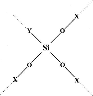
Figure 2. Schematic bonding structure of an adhesion promoter with X and
(⬃2%) for all films during the first hour at 400°C is attributed to moisture desorption since such an abrupt shrinkage was not found during a 30 min degas bake at 400°C in an N2ambient prior to the thermal annealing. It can be seen that both of the aromatic low-k polymers exhibited acceptable thermal stability (⬍5%) at an an-nealing temperature of 400°C. Despite the continual shrinkage for all films at 450°C, the aromatic low-k polymers showed a better thermal stability than did the HSQ film. In particular, the SiLK film revealed the sturdiest thermal stability. This superior thermal stabil-ity of aromatic polymers is presumably due to the incorporation of aromaticity in the polymer backbone.8
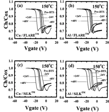
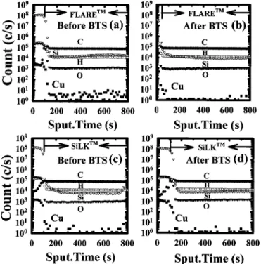
C-V characteristics of oxide-sandwiched low-k polymer capacitors.—Figure 4 presents C-V curves of the Cu as well as the Al electrode FLARE and SiLK oxide-sandwiched MIS capacitors before and after BTS at 150°C for 30 min. For both low-k capaci-tors, we found that the flatband voltage shifts of the Cu electrode capacitors were nearly equal to the corresponding flatband voltage shifts of the Al electrode capacitors. This result indicates that the C-V behavior of the MIS capacitors is irrelevant to the electrode metal used, implying that the negative voltage shifts of the Cu elec-trode capacitors resulting from the positive bias BTS can not be attributed to the presence of Cu ions. These anomalous flatband voltage shifts with either bias polarity are presumably related to the stress induced dielectric polarization charges, to be discussed later. Moreover, two powerful indicators can be easily obtained from two sources when Cu ions readily drift into dielectrics. The first is the reduction of gate current with stress time共Igate-t兲 during the BTS, and the second is extreme increase in gate leakage currents 共Igate-Vgate兲 after the BTS due to the buildup of the Cu ion space charges.8,10-15In this study, however, the gate current characteristics shown in Fig. 5 indicate that there was no transient in gate currents and no distinct difference between the leakage currents in the Al and Cu electrode capacitors. Only intrinsic dielectric conduction current flowed through the dielectric stack, indicating that Cu ions did not penetrate into the polymer layers, and that both FLARE and SiLK polymers individually acted as good dielectric barriers against Cu ions’ drifting under the present stress conditions. Figure 6 shows the
SIMS depth profiles of a number of elements in the Cu electrode oxide-sandwiched FLARE and SiLK MIS capacitors before and af-ter the BTS; the Cu overlayers were removed prior to the SIMS measurement. The presence of Cu was mostly confined within the USG layer, showing the permeation of Cu into the PECVD oxide. The absence of Cu diffusion into the bulk of the polymer further confirmed the barrier capability of both of the low-k polymers against Cu permeation under the present stress conditions. Figure 7 Figure 3. Annealing time dependence of共a兲 and 共b兲 percentage shrinkage of
film thickness, and共c兲 and 共d兲 refractive index for HSQ, FLARE, and SiLK dielectrics annealed at 400 and 450°C.
Figure 4. C-V characteristics of oxide-sandwiched Cu and Al electrode共a兲
and共b兲 FLARE, and 共c兲 and 共d兲 SiLK MIS capacitors stressed at 150°C for
30 min under various positive and negative gate bias.
Figure 5. 共a兲 and 共b兲 current transients during BTS, and 共c兲 and 共d兲
instan-taneous I-V characteristics after BTS for the oxide-sandwiched low-k capaci-tors.
illustrates the distributions of the breakdown field for the TaN/Cu/ 共FLARE, SiLK兲/p-Si MIS capacitors without oxide sandwiching the low-k polymer films thermally annealed at various temperatures. The integrity of the breakdown field after annealing at 450°C addi-tionally confirms the barrier quality of these low-k polymers.
Polarization effects.—Figure 8 shows the stressing time depen-dence of C-V curve shifts for the Al-electrode oxide-sandwiched
low-k capacitors stressed with⫾48 V bias at 150°C. For both bias-ing polarities, the C-V curves made parallel shifts along the voltage axis and the C-V shifts continued even after a prolonged stress of 5 h. Moreover, the negative voltage displacement was dependent on the magnitude of the applied field and that the rate of displacement increased with temperature. This result may imply that either many mobile ions共but not Cu ions兲, or stress induced polarization bound Figure 6. SIMS depth profiles of共a兲 and 共b兲 FLARE and 共c兲 and 共d兲 SiLK
oxide-sandwiched MIS capacitors before and after 48 V/150°C BTS for 30 min; metal electrodes were removed prior to the SIMS measurement.
Figure 7. Breakdown field distributions of共a兲 TaN/Cu/FLARE/Si and 共b兲 TaN/Cu/SiLK/Si capacitors, without oxide sandwiching the low-k polymer films, annealed at various temperatures.
Figure 8. C-V characteristics of Al electrode oxide-sandwiched共a兲 and 共b兲
FLARE, and共c兲 and 共d兲 SiLK capacitors under successive BTS with ⫾48 V bias at 150°C.
charges, inherently reside in the polymer structure.8,16-24A trace of elements共such as sodium兲 at a concentration of less than 1010 cm⫺2 was detected in the studied samples from both XPS and TXRF analyses. However, this concentration is two orders of magnitude less than that necessarily required to produce the observed C-V curve shifts. Furthermore, the absence of both stretch-out and slant distortion in the high frequency C-V curves indicates that the oxide/ silicon interface was relatively free of interface traps that could po-tentially be induced by sodium ions’ drifting to the interface.21,25-28 Therefore, we excluded the possibility of any major charge contri-bution from the mobile ions. Although it was reported that absorbed moisture in the polymer film might yield dielectric moisture polar-ization, we did not observe any evidence regarding the anomalous C-V hysteresis and increased capacitance共or k values兲.8,20 Accord-ingly, the stress induced dielectric polarization bound charges in the bulk of dielectric layers may be reasonably presumed to be respon-sible for the large shift of the C-V curves.共Thermal oxide and USG do not exhibit polarization.兲 These bound charges orientated them-selves under the influence of the electric field and could be charac-terized by a shift of the C-V curve in the same direction as that due to mobile ions. These polarization charges may not exist perma-nently because the C-V curve shifts can be reversed by simply ap-plying a BTS of equal magnitude but opposite polarity, in its electric field. The presence of these bound charges may be attributed to the more polar moieties in the polymer network or potential charge trapping defects in the aromatic backbone of the low-k dielectric.8,29 However, further chemical analyses are needed to clarify their root cause.
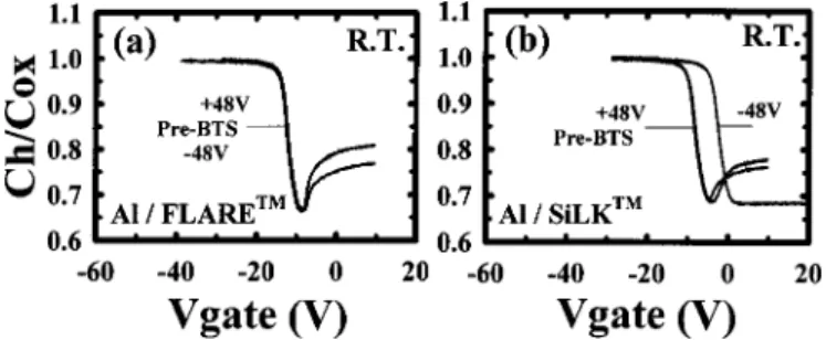
Efforts were made to find the cause of the distinctly different C-V behaviors exhibited by the FLARE and SiLK Al electrode MIS capacitors stressed with a negative bias of⫺48 V at 150°C, in spite of the limits imposed on the sole electrical analysis. First, the posi-tive voltage shift of C-V curves for the FLARE Al electrode capaci-tor was much smaller than that for the SiLK Al-electrode capacicapaci-tor 共Fig. 4b and d兲. Second, the positive voltage shift of the C-V curves for the FLARE Al electrode capacitor reached a saturation value in a stress time of just over 1 h, while this finding was not observed for the SiLK Al electrode capacitor 共Fig. 8b and d兲. Both of the Al electrode FLARE and SiLK capacitors were stressed with⫾48 V bias at room temperature, as shown in Fig. 9 to further clarify these points. A positive voltage shift of about 5 V resulted from the 30 min negative bias stress of⫺48 V for the SiLK sample, while the C-V curve of the corresponding FLARE sample remained stable. The room temperature polarization effect in the SiLK polymer indi-cates the existence of effective stress induced polarization bound negative charges, which were presumably located in the thin adhe-sion layer共Fig. 2兲 inserted between the oxide and the SiLK polymer 共Fig. 1b兲. Figure 10 shows C-V curves for the Al electrode oxide-sandwiched SiLK capacitors, without the adhesion layer, stressed with⫾48 V bias for 30 min at 150°C as well as room temperature. It is clear that without the adhesion layer at the SiLK polymer/oxide interface, the C-V behavior of the SiLK capacitor strongly re-sembles that of the FLARE capacitor共Fig. 4b and 10a at 150°C and
Fig. 9a and 10b at room temperature兲. We found that both FLARE and SiLK polymers were prone to be more strongly affected by the positive bias BTS than by the negative bias BTS, and that they all exhibited the induced polarization effect of strong temperature de-pendence, in the bulk of the low-k polymer. BTS stressing the MIS capacitor at a higher temperature results in a larger negative voltage shift due to the positive bias BTS. The C-V curves of both FLARE and SiLK capacitors remained fairly stable with ⫹48 V BTS at room temperature. Similar temperature-dependent polarization ef-fects of insulators in MIS capacitors have been observed in phos-phosilicate layers (P2O5 polarization兲 and certain vapor-deposited oxides.16,18
Conclusion
Two species of organic aromatic low-k polymers共FLARE and SiLK兲 were evaluated for structural stability against rigorous ther-mal treatment, and for electrical reliability with respect to integra-tion with Cu metallizaintegra-tion. It was found that the thermal stability of SiLK is superior to that of FLARE and HSQ. Although both of the low-k polymers exhibited a fairly good dielectric barrier property against Cu permeation under the stress conditions used in this study, we observed anomalous electrical instabilities in the C-V character-istics. These instabilities are presumably correlated with the stress induced dielectric polarization bound charges under bias tempera-ture stress.
Acknowledgments
The authors wish to give their gratitude to Chau-Chiung Wang, Kuo-Lung Fang, and Chiu-Chih Chiang for their helpful technical assistance.
National Chiao-Tung University assisted in meeting the publication costs of this article.
References
1. L. Peters, Semicond. Int., 1998, 64共Sept兲.
2. The National Technology Roadmap for Semiconductors 1997, Semiconductor In-dustry Association, San Jose, CA.
3. R. A. Donaton, B. Coenegrachts, K. Maex, H. Struyf, S. Vanhaelemeersch, G. Beyer, E. Richard, I. Vervoort, W. Fyen, J. Grillaert, S. V. Groen, M. Stucchi, and D. D. Roest, in Proceedings of 1999 IEEE IITC, p. 262, May 24-26, 1999. 4. L. Peters, Semicond. Int., 2000, 52共Jan兲.
5. L. Peters, Semicond. Int., 1999, 56共Nov兲.
6. Z. C. Wu, C. C. Wang, R. G. Wu, Y. L. Liu, P. S. Chen, Z. M. Zhu, M. C. Chen, J. F. Chen, C. I. Chang, and L. J. Chen, J. Electrochem. Soc., 146, 4290共1999兲. 7. S. U. Kim, T. Cho, and P. S. Ho, in Proceedings of 1999 IEEE IRPS, p. 277, March
23-25, 1999.
8. A. L. S. Loke, J. T. Wetzel, P. H. Townsend, T. Tanabe, R. N. Vrtis, M. P. Zussman, D. Kumar, C. Ryu, and S. S. Wong, IEEE Trans. Electron Devices, ED-46, 2178共1999兲.
9. A. L. S. Loke, C. Ryu, C. P. Yue, J. S. H. Cho, and S. S. Wong, IEEE Electron
Device Lett., EDL-17, 549共1996兲.
10. H. Miyazaki, H. Kojima, and K. Hinode, J. Appl. Phys., 81, 7746共1997兲. 11. G. Raghavan, C. Chiang, P. B. Anders, S. M. Tzeng, R. Villasol, G. Bai, M. Bohr,
and D. B. Fraser, Thin Solid Films, 262, 168共1995兲.
Figure 9. C-V characteristics of Al electrode oxide-sandwiched共a兲 FLARE
and共b兲 SiLK capacitors under BTS with ⫾48 V bias at room temperature for
30 min. Figure 10. C-V characteristics of Al electrode oxide-sandwiched SiLK ca-pacitors, without the adhesion layer between the bottom oxide and SiLK polymer, stressed with⫾48 V bias for 30 min at 共a兲 150°C and 共b兲 room temperature.
19. E. H. Snow and M. E. Dumesnil, J. Appl. Phys., 37, 2123共1966兲. 20. G. Samuelson and S. Lytle, J. Electrochem. Soc., 131, 2717共1984兲.
21. S. M. Sze, Physics of Semiconductor Devices, 2nd ed., Chap. 7, John Wiley & Sons, New York共1981兲.
28. D. K. Schroder, Semiconductor Material and Device Characterization, 2nd ed., Chap. 6, John Wiley & Sons, New York共1998兲.
29. M. Moussavi, G. Passemard, J. C. Maisonobe, and P. Turek, in Proceedings of