國立交通大學
電子工程學系 電子研究所
碩 士 論 文
AXI 匯流排之系統設計與實現
System Design and Implementation of AXI Bus
研 究 生:廖英澤
指導教授:張添烜 博士
AXI 匯流排之系統設計與實現
System Design and Implementation of AXI Bus
研 究 生:廖英澤
Student:
Ying-Ze
Liao
指導教授:張添烜 博士
Advisor:
Dr.
Tian-Sheuan
Chang
國立交通大學
電子工程學系 電子研究所
碩士論文
A ThesisSubmitted to Department of Electronics Engineering & Institute of Electronics
College of Electrical & Computer Engineering
National Chiao Tung University in partial Fulfillment of the Requirements
for the Degree of Master in
Electronics Engineering & Institute of Electronics October 2007
Hsinchu, Taiwan, Republic of China
AXI 匯流排之系統設計與實現
研究生:廖英澤 指導教授:張添烜博士 國立交通大學 電子工程學系 電子研究所摘要
隨著矽智財整合系統單晶片成為可能,整合連結這些矽智財的晶片匯流排成 為整個系統效能上重要的角色,Advanced eXtensible Interface(AXI)是新一代 的晶片匯流排通訊協定,AXI 通訊協定採用封包基準的方式傳輸資料,使用分離 的位址與資料通道,每個通道交握方式使用來源的有效信號與目的的就緒信號在 時脈正緣取樣,當取樣到兩者的訊號皆是 1 則完成交握並傳輸資料,因此可簡單 插入暫存器增加每個通道管線級數來提高工作頻率,另外還支援不需依序完成、 爆發模式傳輸,提供了更高效率的傳輸能力。 在本論文之前並沒有針對新一代晶片匯流排通訊協定上的特性在連結器架 構的硬體成本與頻寬的完整探討,目前已存在的 AXI 匯流排設計都採用交叉開關 (Crossbar Switch)架構,雖然交叉開關提供了高頻寬,但也付出了極高的硬體 成本,使用共享匯流排架構可以減少許多硬體成本,運用 AXI 支援不需依序完成 的特性在共享匯流排上,仍然可以提供相當高的頻寬,因此我們以 SystemC 在交 換層級(Transaction-level)建構了一個可攜式媒體平台(Portable Media Platform)的模型來模擬分析。 由於 AXI 匯流排連接器多了一層的暫存器,交握時為了確保資料傳輸正確, 在一般的傳輸模式下頻寬的最高使用率只有 50%,針對這點在本篇論文我們設計 了交錯傳輸模式(Interleaved Mode)來提高頻寬使用率最高達 99%。此模式的使 用只要連接器提供支援即可,完全不需要協定上的修改。此外,對於系統中有高 初始延遲的記憶體控制器裝置,我們另外設計了資料通道鎖定模式(Data Lock Mode)以及混合傳輸模式(Hybrid Mode),可以有效地減少記憶體資料傳輸時間, 也給予記憶體控制器高度重新排程的能力,以提高頻寬使用率並進而提昇系統的 效能。 在建構的平台上我們驗證了所提出的各種傳輸模式在真實系統環境下的效 用,除此之外,實驗中探討了 AXI 介面緩衝器大小、仲裁策略、傳輸模式以及仲 裁權重調整方式對系統效能的影響,實驗結果證明在適當傳輸模式配置和系統配 置下,可以提高 69%的頻寬使用量、進而提升 40%的系統速度。另外相較於傳統 不支援不需依序完成功能的匯流排如 AHB,AXI 匯流排搭配前述提出的傳輸模式與系統配置,最多可以提高 346%的頻寬使用率及 44%的系統速度。這顯現出採用 AXI 匯流排並恰當地搭配各種傳輸模式可以大幅度並有效地改善系統效能。
最後我們做成實際的硬體,在 0.13 微米的互補式金氧半導體製程下,在 200 百萬赫茲的運作頻率下需要 18.85K 個邏輯閘,提供使用每一千個邏輯閘每秒 84MB 的頻寬。
System Deign and Implementation of AXI Bus
Student: Ying-Ze Liao Advisor: Dr. Tian-Sheuan ChangDepartment of Electronics Engineering & Institute of Electronics National Chiao Tung University
Abstract
The on-chip-bus (OCB) which connects silicon intellectual property (SIP) in a system-on-a-chip (SoC) plays a key role in affecting the system performance. Recently, a new generation of packet-based OCB protocol called Advance eXtensible Interface (AXI) has been proposed. The AXI separates the address and data into independent channels. The handshaking of each channel uses two signals which one is VALID from source and the other is READY from destination. Once the VALID and READY are high at the same clock positive edge, the handshaking completed and data transferred. Therefore, it is easy to add pipeline stage to increase operating frequency by inserting the register slice. Besides, the AXI protocol supports out-of-order completion and burst-based transaction to provide more bandwidth than traditional OCB protocol.
Before this thesis, there is no complete analysis on the interconnect architecture and bandwidth of the of new generation OCB protocol. The existed AXI bus interconnect all adopt the crossbar switch as the architecture. Although the crossbar switch provides high bandwidth, it needs extreme hardware cost. Using the characteristic of AXI, we can adopt the shared bus as the architecture of the bus interconnect to obtain low hardware cost and keep fairly high bandwidth. To analyze impact of the architecture, a portable media platform (PMP) is modeled at transaction-level with SystemC for simulations.
However, the AXI bus interconnect can only achieve 50% of bandwidth utilization at most when normal transfer mode is being used. Therefore, we propose an interleaved transfer mode to increase the bandwidth utilization up to 99%. The interleaved transfer mode can be implemented as a totally built in feature of a bus interconnect and does not need any modification to the protocol. In addition, this work also proposes a data lock transfer mode and hybrid mode to handle the transactions to the devices with long initial access latency, such as the memory controller in a system. These modes decrease the transfer time and give the memory
controller a higher degree of access rescheduling capability.
We evaluate impact of the proposed transfer modes in the portable media platform. In addition, the impact of wrapper buffer size, arbitration policy, transfer mode setting, and arbitration parameter settings are also studied. The simulation result shows that the proposed transfer modes improve the bandwidth utilization by 69% and speed up the system by 44%. Compare the performance with the traditional bus such as the AHB; the AXI system can outperform the AHB system in bandwidth utilization by 346% and system speed by 44% at most.
The implemented AXI bus interconnect with the proposed transfer modes has a gate count of 18.85K when synthesized with 0.13μm CMOS process under 200 MHz operating frequency.
致 謝
首先誠摯的感謝指導教授張添烜博士,老師耐心的教導使我學習到做 研究的方法,不時的討論並指點我正確的方向,使我在這些年中獲益匪淺。 本論文的完成另外亦得感謝張彥中學長的大力協助,因為有你細心地 跟我討論與我反覆的檢討,使得本論文能夠更完整而嚴謹。 在兩年的日子裡,實驗室裡共同的生活點滴,有學術上的討論與生活 經驗的分享。非常感謝眾位學長、同學、學弟的共同砥礪,你們的陪伴讓 這兩年的研究生活變得絢麗多彩。 感謝林佑昆、蔡旻奇、古君偉、王裕仁、余國亘、吳錦木學長們不厭 其煩的指出我研究中的缺失,且總能在我迷惘時為我解惑,也感謝林嘉俊 同學與我參加了兩年的 IC 競賽,使得我在設計 IC 的技巧更成熟,另外也 感謝吳秈景、郭子筠、李得瑋同學給予我的鼓勵,恭喜我們順利走過這兩 年。實驗室的蔡宗憲、曾宇晟、詹景竹、張瑋城、戴瑋呈學弟們當然也不 能忘記,你們的幫忙及搞笑我銘感在心。 最後,謹以此文獻給我摯愛的雙親。Content
Chapter 1 Introduction ...1
1.1 Background ...1
1.2 Related Work...2
1.3 Motivation and Contribution...3
1.4 Thesis Organization ...3
Chapter 2 Overview of the AMBA Bus ...4
2.1 AHB ...4
2.1.1 AHB Architecture ...4
2.1.2 AHB Handshaking and Arbitration...5
2.2 AXI ...7
2.2.1 AXI Architecture...8
2.2.2 Channel Handshaking ...10
2.2.3 Transaction Ordering ...12
2.3 Comparison between AXI and AHB...13
2.3.1 Protocol and Architecture ...13
2.3.2 Latency and Bandwidth Utilization ...13
2.3.3 Hardware Cost ...15
Chapter 3 Simulation Modeling for AXI System ...20
3.1 Overview of the Modeling Method...20
3.1.1 Transaction-Level-Modeling ...20
3.1.2 Using SystemC as Modeling Language...21
3.2 Traffic Generation...22
3.3 AXI Master ...24
3.3.1 Master Behavior Modeling ...24
3.3.2 Master Types ...25
3.3.3 States of Mater Processing Transaction ...28
3.4 AXI Slave...30
3.4.1 Slave Types ...30
3.4.2 States of Slave Processing Transaction...31
Chapter 4 Design of AXI Bus Interconnect...34
4.1 Bus Interconnect ...34
4.2 Transfer Mode...36
4.2.1 Normal Mode ...39
4.2.2 Interleaved Mode ...39
4.2.3 Data Lock Mode ...40
4.3 Arbitration Policy...45
4.3.1 Our AXI Arbitration Flow...45
4.3.2 Fixed Priority ...46
4.3.3 TDMA...47
4.3.4 Round-Robin...48
4.3.5 Lottery...49
Chapter 5 Simulation and Analysis...51
5.1 Introduction...51 5.2 PMP Platform...52 5.2.1 Overview...52 5.2.2 Scenario...54 5.3 Experiments ...55 5.3.1 Performance Metric ...55
5.3.2 Simulation of Video Phone Scenario ...56
5.4 AXI vs. AHB...75
5.4.1 AHB PMP Platform ...75
5.4.2 Comparison between AXI and AHB...76
Chapter 6 Hardware Implementation...80
6.1 Hardware Design ...80
6.1.1 Read Transaction Design ...80
6.1.2 Write Transaction Design...81
6.2 Implementation Results ...82
Chapter 7 Conclusion and Future Works ...84
7.1 Conclusion ...84
7.2 Future Works...84
List of Figures
Fig. 2-1 AHB architecture ...5
Fig. 2-2 AHB simple transfer ...6
Fig. 2-3 Transfer with wait states ...6
Fig. 2-4 AHB arbitration...7
Fig. 2-5 Generic AXI architecture ...8
Fig. 2-6 Read transaction...9
Fig. 2-7 Write transaction ...10
Fig. 2-8(a)VALID before READY (b)READY before VALID (c)VALID with READY...12
Fig. 2-9 AHB continuous transfer ...14
Fig. 2-10 AXI continuous transfer...14
Fig. 2-11 AHB burst transaction...15
Fig. 2-12 AXI burst transaction ...15
Fig. 3-1 System Modeling Graph ...21
Fig. 3-2 Illustration of a modeling module...22
Fig. 3-3 Illustration of traffic generation ...22
Fig. 3-4 Example of a task state table file ...24
Fig. 3-5 Flow of transaction generation in master...25
Fig. 3-6 Regular type master (a) block diagram (b) Flow of ProcPTT() ...26
Fig. 3-7 DMAC type master (a) block diagram (b) Flow of ProcPTT() ...27
Fig. 3-8 MPU type master (a) block diagram (b) Flow of ProcPTT() ...28
Fig. 3-9 FSM of master’s PTT...29
Fig. 3-10 Block diagram of regular type slave ...30
Fig. 3-11 Block diagram of MEM type slave ...31
Fig. 3-12 FSM of transaction in slave read PTT ...32
Fig. 3-13 FSM of transaction in slave write PTT ...33
Fig. 4-1 Shared bus architecture ...34
Fig. 4-2 Multi-layer architecture ...35
Fig. 4-3 Crossbar architecture ...36
Fig. 4-4 Register slice of AXI bus interconnect ...37
Fig. 4-5 Error case of data transfer ...38
Fig. 4-6 Correct case of data transfer ...38
Fig. 4-7 Timing diagram of normal mode ...39
Fig. 4-8 Timing diagram of interleaved mode...40
Fig. 4-9 Timing diagram of data lock mode ...41
Fig. 4-11 Flow of hybrid mode...45
Fig. 4-12 Flow of our arbitration...46
Fig. 4-13 Illustration of TDMA policy ...48
Fig. 4-14 Illustration of Round-Robin policy...49
Fig. 4-15 Example of lottery arbitration...50
Fig. 5-1 AXI PMP platform ...52
Fig. 5-2 Completion time of video phone with all normal transactions ...60
Fig. 5-3 Bandwidth utilization of video phone with all normal transactions ...60
Fig. 5-4 Completion time of video phone with setting 1...63
Fig. 5-5 Bandwidth utilization of video phone setting 1 ...63
Fig. 5-6 Completion time of video phone with setting 2...65
Fig. 5-7 Bandwidth utilization of video phone setting 2 ...65
Fig. 5-8 Average completion time of different task setting ...66
Fig. 5-9 Average bandwidth utilization of different task setting ...67
Fig. 5-10 Average Latency of Different Task Setting...67
Fig. 5-11 Completion time of video phone with data lock buffer 2 ...69
Fig. 5-12 Bandwidth utilization of video phone with data lock buffer 2 ...70
Fig. 5-13 Completion time of video phone with data lock buffer 4 ...71
Fig. 5-14 Bandwidth utilization of video phone with data lock buffer 4 ...72
Fig. 5-15 Average bandwidth utilization of weight tuning...74
Fig. 5-16 Standard deviation of bandwidth utilization of weight tuning...74
Fig. 5-17 AHB PMP platform...75
Fig. 5-18Completion time of AXI and AHB ...78
Fig. 5-19 Bandwidth utilization of AXI and AHB ...79
Fig. 5-20 Average latency of AXI and AHB...79
Fig. 6-1 Block diagram of read transaction design...81
List of Table
Table 2-1 Main difference between AXI and AHB ...13
Table 2-2 Parameters for hardware cost calculation...16
Table 2-3 Comparison of hardware cost between AHB and AXI...19
Table 3-1 Fields of a task state ...23
Table 4-1 Limitation of bandwidth utilization using data lock mode...44
Table 5-1 Master configuration of PMP platform ...53
Table 5-2 Slave configuration of PMP platform...53
Table 5-3 Performance of AXI PMP platform...54
Table 5-4 Task of video phone scenario ...55
Table 5-5 Factor of configuration...57
Table 5-6 Setting of simulation A...58
Table 5-7 Timing constraint status with all normal transaction of video phone scenario ...59
Table 5-8 Configuration of simulation B...61
Table 5-9 Configuration of data lock mode of simulation B...61
Table 5-10 Timing constraint status with setting 1 of video phone scenario ...62
Table 5-11 Timing constraint status with setting 2 of video phone scenario...64
Table 5-12 Configurations of simulation for data lock mode buffer size...68
Table 5-13 Timing constraint status with data lock mode buffer 2 ...68
Table 5-14 Timing constraint status with data lock mode buffer 4 ...70
Table 5-15 Configuration of weight tuning ...73
Table 5-16 Met configurations of buffer size 4 in weigh tuning ...75
Table 5-17Performance of AHB PMP platform ...76
Table 5-18 ...77
Chapter 1 Introduction
1.1 Background
Recently, VLSI technology has improved significantly and more transistors can be integrated into a chip. This makes the ideal of system-on-a-chip [1] more of an achievable goal than an abstract dream. However, along with the increasing transistor count comes along the increasing design and verification complexities. Although EDA tools have also been developed in hope of helping system designer to handle the massive complexity, proper system-level design and verification methodology have played a much more important role. One such methodology is the platform-based design methodology which uses pre-verified silicon intellectual property (SIP) and an on-chip-bus (OCB). The OCB connects SIPs and provides communication among SIPs.
Since OCB is often the bottleneck of a system, a good OCB protocol plays an important role. One of the industry’s de facto standard bus protocols is ARM’s Advanced High-performance Bus (AHB). AHB is an OCB which adopts traditional bus architecture. It transfers the data in a pipeline way and completes the transaction in order. The exploration of AHB has been done for years [2]~ [4], which includes architecture, low power and arbitration policy . However, Advance eXtensible Interface (AXI) is the successor of AHB but the study on AXI is still few. AXI contains lots of features which improves the performance of the OCB, such as packet-based transfer, out-of-order completion, and single address transaction. However, the related research of AXI is rare and lacks comparison with AHB. Thus, a complete analysis of AXI is necessary.
1.2 Related Work
In a system design, the bus arbitration policy plays an important role. The traditional arbitration policies include fixed priority, Round-Robin, and time division multiple access (TDMA) [5]. The fixed priority is the simplest policy which uses a static priority to arbitrate when contention occurs, but it has a fatal drawback that starvation. The Round-Robin and TDMA solve the starvation and provide a fair arbitration. In addition, There is a novel one: lottery [6] which is a probability-based arbitration policy. The lottery provides a good bandwidth allocation than the other polices. Mixing these polices brings out various characteristic of polices. However, in these papers, they mostly focus the analysis on the arbitration policy itself but lack a complete analysis on a system platform running a real application. Being aware of this, Poletti [6] [5] builds an AHB platform and uses various patterns to analyze the impact of the fixed priority, TDMA, Round-Robin, and a time-slot reserve arbitration. Later, Lee [7] builds a shared bus AHB platform and a crossbar AXI platform to evaluate the performance of the two platforms. The comparison between the two platforms reveals that AXI bus has a superior performance. With the multi-core system becoming a trend, Ruggiero [8] builds a multi-core system with AHB, AXI and STBus to analyze the scalability of modern OCB protocol. Although the new generation OCB protocol has been analyzed in these two papers, their AHB bus architectures all adopt the shared bus and their AXI bus architectures adopt the crossbar, hence the comparison is not fair and the hardware cost is not taken into consideration. In addition, their arbitration policy in AXI bus interconnects are fixed priority so the potential of AXI may not have been fully explored. Until now, there has been no thorough analysis and exploration on AXI’s arbitration policy, architecture, and hardware cost.
1.3 Motivation and Contribution
The issues mentioned above motivate us to investigate the performance of AXI bus in a system platform running an application. Being aware of the cost difference between the share bus and crossbar architecture, we focus our investigation in share bus architecture. In addition, the analysis result of using basic transfer which showed poor performance also motivated us to propose more efficient AXI transfer mode. Finally, the question of whether AHB or AXI is better for a system motivates us to conduct comparison on their performance and cost.
The contribution of this thesis includes the following.
1. The designed Transaction Level Models (TLM) are able to build various platforms and perform various scenarios to evaluate the system performance and to obtain proper configuration.
2. We analyze the impact of the AXI on various arbitration policies. 3. We give a proper way to design a shared bus AXI bus interconnect.
4. The designed AXI bus interconnect provides high bandwidth and low hardware cost
1.4 Thesis Organization
In chapter 2, we give a brief overview of the AMBA bus protocol. In chapter 3, we describe the methods we used in modeling AXI system. In chapter 4, we proposed an AXI interconnection which is able to provide high bandwidth and configuration of arbitration policy. In chapter 5, we show the result of simulation and analysis. In chapter 6, we implement the AXI interconnection hardware according to result of chapter 5. Chapter 7 is the conclusion and future works.
Chapter 2 Overview of the AMBA Bus
2.1 AHB
Advanced High-performance Bus (AHB) was proposed in AMBA 2.0 in 1999 and has been widely adopted since. Since then, AHB has been regarded as the industries de facto on-chip communication protocol. The basic architecture and protocol are described in this sub section. The features of AHB list below:
z Pipelined transfer z Burst transfer
z Single-cycle bus master handover z Single-clock edge operation z Non-tri-state implementation
z Wider data bus configurations (64/128 bits)
2.1.1 AHB
Architecture
Fig. 2-1 shows the simplified AHB architecture which contains masters, slaves, arbiter, decoder and mux.
Each master and slave has three ports which are HADDR, HWDATA and HRDATA. HWDATA and HRDATA share the signal “HADDR” to indicate the destination of data transfer and therefore there is only one date transfer which is either HWDATA or HRDATA.
In the specification of AHB, it defined that bus interconnect is composed of arbiter, decoder and mux and the bus ownership is controlled by the centralized
arbiter to guarantee that only one master can use the shared bus. Master #1 Slave #1 Arbiter Decoder Master #2 Master #3 Slave #2 Slave #3 Slave #4 HADDR HADDR HADDR HWDATA HWDATA HWDATA HRDATA HRDATA HRDATA HRDATA HADDR HWDATA HRDATA HADDR HADDR HADDR HRDATA HWDATA HWDATA HRDATA HWDATA Address and control mux
Write data mux Read data mux
REQ REQ REQ GRANT#1 GRANT#2 GRANT#3
Fig. 2-1 AHB architecture
2.1.2 AHB
Handshaking
and
Arbitration
Each transaction of AHB contains two phases which are address phase and data phase as shown in Fig. 2-1. The address phase and data phase are sent in pipelined order, which means that data can only be sent after its address has been sent. This pipelined mechanism is controlled by the signal “HREADY”. If HREADY is high, no
pipeline stall is introduced; otherwise, a pipelined stall is introduced as shown in Fig. 2-3.
Fig. 2-2 AHB simple transfer
Fig. 2-3 Transfer with wait states
The ownership of the bus is controlled by a centralized arbiter. Fig. 2-4 shows an example of the arbitration process. First, each master sends a request to the arbiter by pulling HBUSREQ high. After several cycles, the arbiter asserts HGRANT but the
ownership of the bus still has not changed. Once both HGRANT and HREADY are high (Fig. 2-4,cycle T5), the granted master gets the ownership of bus. The ownership of the bus would remain until its transaction has been completed.
Fig. 2-4 AHB arbitration
2.2 AXI
Advanced eXtensible Interconnect (AXI) was introduced in AMBA 3.0 as the successor on-chip bus protocol of the AHB in AMBA 2.0. The basic architecture and protocol are introduced in this sub section. The AXI protocol is targeted at high-performance, high-frequency system designs and includes a number of features that make it suitable for high-speed submicron interconnect.
The key features of the AXI are:
z Separate address/control and data phases
z Support for unaligned data transfer using byte strobes z Burst-based transaction with only start address issued
z Separate read and write data channels to enable low-cost Direct Memory Access
z Ability to issue multiple outstanding addresses z Out-of-order transaction completion
z Easy addition of registers stages to provide timing closure
2.2.1 AXI
Architecture
Fig. 2-5 shows a generic AXI architecture. There are five independent channels which communicate with master and slave. The five channels are read address channel, write address channel, read data channel, write data channel and write response channel. Each channel has a set of forward signals and one feedback signal for handshaking.
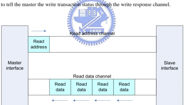
Fig. 2-6 shows an AXI read transaction. When an AXI master performs a read transaction, it sends a read address transfer which contains a start address and control information through the read address channel to a slave. When the slave accepts the address and control transfer, it starts its process according to the transfer accepted. Once the slave completes its process, it sends the data requested by the master through the read data channel. This transaction is not done until the master accepted the last burst data which contains read transaction status.
Fig. 2-7 shows an AXI write transaction. A master sends a write address transfer which also contains a state address and control information through the write address channel to a slave. Then, the master sends write data to the slave through the write data channel. After the slave accepted all write data, the salve sends a write response to tell the master the write transaction status through the write response channel.
Fig. 2-7 Write transaction
2.2.2 Channel
Handshaking
Each channel has a VALD and READY signals for handshaking. The source asserts VALID when the control information or data is available. The destination asserts READY when it can accept the control information or data. Transfer occurs only when both the VALID and READY are asserted. Fig. 2-8 shows all possible cases of VALID/READ handshaking. Note that when source asserts VALID, the corresponding control information or data must also be available at the same time. The arrows in Fig. 2-8 indicate when the transfer occurs.
A transfer takes place at the positive edge of clock. Therefore, the source needs a register input to sample the READY signal. In the same way, the destination needs a register input to sample the VALID signal. Considering the situation of Fig. 2-8(c), we assume the source and destination use output registers not combination circuit,
they need one cycle to pull low VALID/READY and sample the VALID/READY again at T4 cycle. When they sample the VALID/READY again at T4, there should be another transfer which is an error. Therefore source and destination should use combinational circuit as output. In short, AXI protocol is suitable register input and combinational output circuit.
(a)
(C)
Fig. 2-8(a)VALID before READY (b)READY before VALID (c)VALID with READY
2.2.3 Transaction
Ordering
Unlike AHB which only allows one granted transaction to access the bus interconnect until this transaction is finished, AXI allows granted transactions to access bus interconnect simultaneously. AXI uses “ID tag” to identify different transactions and enables out-of-order transaction completion.
Out-of-order transaction completion improves system performance in two ways: z Bus interconnect allows the transactions to fast slave to complete in advance
without waiting for the completion of the transaction to slow slave.
z Complex slave can return read data which is available for later transaction without waiting data of prior transaction.
AXI supports out-of-order transaction completion but it doesn’t mean that there is no restriction of reordering transactions. The rule is “Transactions with the same ID must be completed in order”. In other words, if a master requires multiple transactions to be completed in order, the master must assign the same ID to these transactions. If there is no restriction on in-order transaction completion, a master can assign different IDs to those transactions.
system, bus interconnect must append additional master ID to each transaction so that each transaction becomes unique in the system.
2.3 Comparison between AXI and AHB
2.3.1 Protocol
and
Architecture
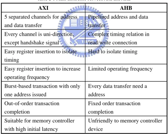
Table 2-1 shows the main difference of protocol and architecture between AXI and AHB. There are seven key points as shown in below:
Table 2-1 Main difference between AXI and AHB
AXI AHB
5 separated channels for address and data transfer
Pipelined address and data transfer
Every channel is uni-direction, except handshake signal
Complex timing relation in read/write connection Easy register insertion to isolate
timing
Hard to isolate timing
Easy register insertion to increase operating frequency
Limited operating frequency
Burst-based transaction with only one address issued
Every data transfer need a address
Out-of-order transaction completion
Fixed order transaction completion
Suitable for memory controller with high initial latency
Unfriendly to memory controller device
2.3.2 Latency and Bandwidth Utilization
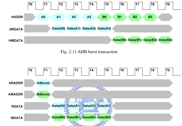
The separate channels in AXI provide less latency in transfer task of read/write transaction pair than AHB. The reason is that AXI is able to perform read and write
transactions at the same time. Fig. 2-9 and Fig. 2-10 show the difference in AHB and AXI transferring the same task. Fig. 2-9 shows AHB’s continuous transfer. There are four read data transfers and four write data transfers. Form Fig. 2-9, all eight data transfers spend eight cycles from T2 to T9. Fig. 2-10 shows the same task in AXI bus. In AXI case, it only spends four cycles form T2 to T5.
Fig. 2-9 AHB continuous transfer
Fig. 2-10 AXI continuous transfer
As for the bandwidth utilization, AXI is more efficient than AHB. The reason is the same with the case of latency. Fig. 2-11 and Fig. 2-12 show the difference of AHB and AXI. In Fig. 2-11 and Fig. 2-12, AHB and AXI perform four beats read burst transaction and a four bests write burst transaction respectively. AHB totally takes eight cycles to complete these two transactions and the bandwidth utilization of data bus HRDATA/HWDATA is only 50%. As to AXI, it only takes four cycles to complete transactions and the bandwidth utilization of data bus RDATA/WDATA is 100%. The bandwidth utilization of AHB is naturally 50% and AXI can increase
bandwidth utilization to 100% based on transferring read/write transaction pair. In short, AXI is capable to perform read/write transaction pair which improves the latency of transaction and bandwidth utilization.
Fig. 2-11 AHB burst transaction
Fig. 2-12 AXI burst transaction
2.3.3 Hardware
Cost
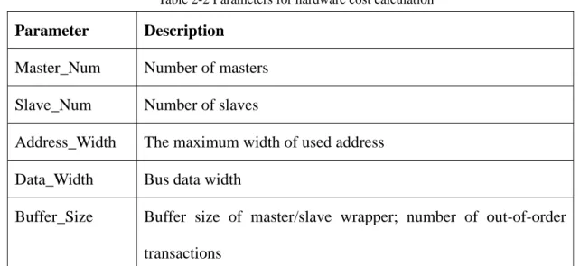
In this section, we analyze the protocol of AXI and AHB to estimate the hardware cost of them based on the amount of mux and register which they used. Table 2-2 is the parameters defined for the hardware cost calculation and the following are the formula for hardware cost. The constants in the formula are indispensable bits.
Table 2-2 Parameters for hardware cost calculation
Parameter Description
Master_Num Number of masters Slave_Num Number of slaves
Address_Width The maximum width of used address Data_Width Bus data width
Buffer_Size Buffer size of master/slave wrapper; number of out-of-order transactions
AHB master port register
Width Data
ster _Port_Regi
AHB_Master =4+ _
AHB slave port register
⎡
Master Num⎤
Width Data Width Address ter Port_Regis AHB_Slave_ =11+ _ + _ + log2 _AHB arbiter register
2 _
_
24+ + ×
= Address Width Master Num
r_Register AHB_Arbite
AHB master buffer register
16 _
_
9+ + ×
= Address Width Data Width
gister _Buffer_Re AHB_Master
AHB slave buffer register
16 _
_
9+ + ×
= Address Width Data Width ster
BufferRegi AHN_Slave_
AXI master port register
⎡
log _⎤
2 _10+ + 2 ×
= Data Width Buffer Size
ster _Port_Regi AXI_Master
AXI slave port register
⎡
⎤ ⎡
(
log _ log _)
3 _ 2 _ 46+ × + + 2 + 2 × = Num Master Size Buffer Width Data Width Address te⎤
r Port_Regis AXI_Slave_AXI interconnection master port register
⎡
log _⎤
3 _ 2 _ 46 _ _ 2 × + + × + = Size Buffer Width Data Width Address Register Port ter onnect_Mas AXI_IntercAXI interconnection slave port register
⎡
⎤ ⎡
(
log2 _ log _)
2 _ 10 _ _ _ _ 2 × + + +⎤
= Size Buffer Num Master Wdith Data Register Port Slave ct Interconne AXIAXI interconnection WDATA table register
⎡
Slave Number⎤
Size Buffer Num Master Table WDATA ct Interconne AXI _ _ _ = _ × _ × log2 _AXI master buffer register
(
Address Width Data Width)
Buffer Sizeister Buffer_Reg Master AXI _ 16 _ _ 18 _ _ × × + + =
AXI slave buffer register
⎡
⎤ ⎡
⎤
(
Buffer Size Master Num Address Width Data Width)
Buffer Sizeister Buffer_Reg Slave AXI _ 16 _ _ _ log _ log 17 _ _ 2 2 + + + × × + =
AHB Master_Num to 1 mux
Wdith Data Width Address Mux to num Master AHB_ _ _ _1_ =15+ _ + _
AHB Slave_Num to 1 mux
Wdith Data Mux to num Slave AHB_ _ _ _1_ =19+ _
AXI Master_Num to 1 mux
⎡
Buffer Size⎤
Address Width Data WidthMUX to Num Master AXI _ 2 _ 3 _ log 41 _ 1 _ _ _ _ 2 × + × + + =
AXI Slave_Num to 1 mux
⎡
Buffer Size⎤
Data Width MUXto Num Slave
AXI _ _ _ _1_ =5+ log2 _ ×2+ _
According to the formula, we give a system to compare the hardware cost between AXI and AHB. The system consists of 5 masters, 11 slaves and AHB system has one buffer and AXI system has eight buffers. The arbitration policy in system is fixed priority so we ignore the registers in arbiter. If we ignore the register used in master and slave buffer, the hardware cost of AXI is 3.18 times of AHB. The hardware cost of AXI is more than AHB indeed.
Table 2-3 Comparison of hardware cost between AHB and AXI AHB 1 buffer AXI 8 buffer 1 master port 36 48 1 slave port 78 160
Wrapper interface register
Total 114 208
AHB arbiter 66 n/a
AXI interconnection 1 master port 151 AXI interconnection 1 Slave port 54 AXI WDATA table
n/a 160 Interconnection register Total 66 365 1 master buffer 553 562 1 slave buffer 553 567
Wrapper buffer register
Total 1106 1129
Master_Num to 1 mux 79 146
Slave_Num to 1 mux 51 43
Interconnection mux
Total 130 189
System register without buffer 5 master, 11 slave 1104 3509 System register with buffer 5 master, 11 slave 2210 12541
Chapter 3 Simulation Modeling for AXI
System
3.1 Overview of the Modeling Method
3.1.1 Transaction-Level-Modeling
Transaction-level-modeling (TLM) [9] is a popular method to modeling a system. There are many kind of modeling level in modeling a system as shown in Fig. 3-1. We choose the node D in Fig. 3-1 as our modeling level. The communication model is modeled at transaction abstraction level. The computation model is modeled at behavior level, but we do not model the functions because of that our emphasis is on the bus communication. Choosing the node D, we check the correctness of bus protocol but also obtain precise analysis of system performance.
A read/write transaction on the AXI protocol can be decomposed into address/control transfer, data transfers and response transfer. Each transfer we used is referred as the transaction on each channel. This is because of supporting the AXI’s capability of out-of-order transaction completion so we treat each transfer as an independent transaction and provide a cycle accurate timing transaction-level-modeling to archive our goal.
Fig. 3-1 System Modeling Graph
3.1.2 Using SystemC as Modeling Language
We use SystemC [11] as our modeling language. SystemC has been widely used to model system at various abstraction levels. The reason we decided to use SystemC is because the timing simulation kernel and primitives are already available. SystemC is also a subset of C++ so that we can also use regular C++ expressions. It’s easy to use and there’s no need to learn another language.
Fig. 3-2 shows how we use model a module using SystemC. The communication interface is implemented using SystemC input and output port. The SystemC processes related to the communication interface are implemented using SystemC method with clock edge trigger. Other internal SystemC processes are also implemented using SystemC method but some are event driven instead of clock driven. In addition to SystemC processes, there are also C/C++ processes inside the module. These un-timed processes implement basic computation and functionality whereas the SystemC processes provide cycle accurate behavior.
Fig. 3-2 Illustration of a modeling module
3.2 Traffic Generation
In this section, we introduce our traffic generation. The bus traffic is generated on transaction basis. Each transaction is generated by a bus access task which is associated with master device. Each master device possesses multiple bus access tasks. Many bus access tasks comprise a task state table (TST). In other words, each master device generates transactions from a task of TST as shown Fig. 3-3.
Fig. 3-3 Illustration of traffic generation
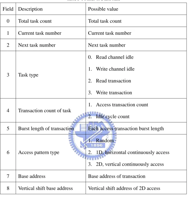
In the task state table, each task describes a set of transactions with the same direction and address pattern. Table 3-1 shows the fields of a task which includes current task number, next task number, task type, task transaction count, transaction burst length, pattern type, base address and vertical shift base address.
Table 3-1 Fields of a task state Field Description Possible value
0 Total task count Total task count 1 Current task number Current task number 2 Next task number Next task number
3 Task type
0. Read channel idle 1. Write channel idle 2. Read transaction 3. Write transaction
4 Transaction count of task
1. Access transaction count 2. Idle cycle count
5 Burst length of transaction Each access transaction burst length
6 Access pattern type
1. Random
2. 1D, horizontal continuously access 3. 2D, vertical continuously access 7 Base address Base address of transaction
8 Vertical shift base address Vertical shift address of 2D access
Fig. 3-4 is an example of a task state table file. The total task count is 24000. We take the row 8 of Fig. 3-4 as a example to explain how a set of transactions are generated from a task. The current task number is 6 and next task number is 7 meaning that when this task 6 finished it will take task 7 as next task. The remainder information means that this task generates 4 read transaction with burst length 16, base address 0x2001EF00 and the base address of each transaction shifts a base address 320.
This transaction generation using task state description allows us to specify bus access behavior at task level. In contrast to specify each transaction individually, we can specify related transaction using only one task. In other words, the traffic description can be greatly reduced by using task level description.
1
2
3
4
5
6
7
8
0
Fig. 3-4 Example of a task state table file
3.3 AXI Master
This subsection describes how to model master devices.
3.3.1 Master
Behavior
Modeling
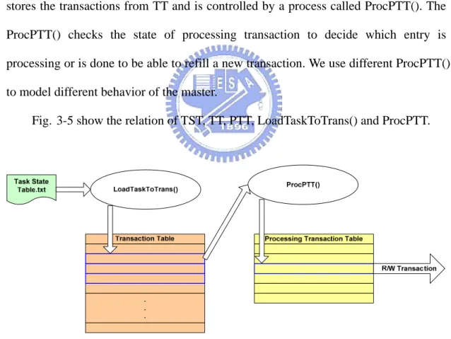
To model the behavior of a master device, we use task state table (TST), transaction table (TT) and processing transaction table (PTT) to control the master device’s behavior.
A. Task State Table
The task state table has mentioned in previous section. It is used to store all tasks of a master. However, a master may have multiple TST.
B. Transaction Table
The transaction table exists in each master and each transaction table is associated with a TST. It is used to store the transactions which are generated by the tasks. Once the master device is reset, there is a process called LoadTaskToTrans() which starts to load all tasks and generates all transactions to store into TT.
C. Processing Transaction Table
The processing transaction table actually is the buffer of a master device. The entry of it is a processing transaction which is a state machine. The detail of processing transaction will describe in later section. The processing transaction table stores the transactions from TT and is controlled by a process called ProcPTT(). The ProcPTT() checks the state of processing transaction to decide which entry is processing or is done to be able to refill a new transaction. We use different ProcPTT() to model different behavior of the master.
Fig. 3-5 show the relation of TST, TT, PTT, LoadTaskToTrans() and ProcPTT.
Fig. 3-5 Flow of transaction generation in master
3.3.2 Master
Types
behaviors. They are regular type, DMAC type and MPU type.
A. Regular Type
Fig. 3-6(a) shows the block diagram of a regular type master. It only contains a prime task state table so its behavior is very simple as shown in Fig. 3-6(b). It processes a prime task and sends the IRQ to MPU when it completes a prime task. After the repeat count reached the value set in advance, the master stopped. The examples of regular type masters are DSP, video encoder and etc.
End done/send IRQ Processing prime task transaction Start Prime task
need repeat? yes
no
(a) (b)
Fig. 3-6 Regular type master (a) block diagram (b) Flow of ProcPTT()
B. DMAC Type
Fig. 3-7 shows the block diagram and state machine of DMAC type master. It contains multiple task state tables so its behavior is more complex than regular type master. Each task has its own a repeat counter which stores how many times it need to repeat and an active counter which uses to active the task periodically. When the task completes, the master sends the corresponding IRQ to MPU and resets the active
counter. After all tasks done and reached the repeat counts, the master stopped. Processing #0 task transaction Start End
done/send IRQ 0 and reset active counter Processing #1 task transaction Processing #2 task transaction #0 active and need repeat ? #1 active and need repeat ? #2 active and need repeat ? All done? yes no yes no yes no yes no
done/send IRQ 1 and reset active counter
done/send IRQ 2 and reset active counter
(a) (b)
Fig. 3-7 DMAC type master (a) block diagram (b) Flow of ProcPTT()
C. MPU Type
Fig. 3-7(a) shows the block diagram of MPU type master. It is much different form the regular type and DMAC type. MPU type master not only processes prime task but also accepts external IRQ to execute corresponding ISR task as shown in Fig. 3-8(b). In the behavior of MPU, the priority of ISR is higher than prime task so the ISR task can interrupt the process of prime task. When MPU completes the all prime tasks, it gets into the idle state, but still waits for accepting the IRQ.
(a) (b) Fig. 3-8 MPU type master (a) block diagram (b) Flow of ProcPTT()
3.3.3 States of Mater Processing Transaction
The processing transaction in PTT is a state machine. We use the states to control the transaction’s status. There are six states in master’s processing transaction including empty/done, read request, read data, write request, write data and write response.
A. Empty/done
The state of processing transaction in PTT is empty in the initial. When any transaction completed, the state became to done. This state means the initial and finish state, and is ready to be filled transaction from transaction table by ProcPTT() process. According to the filled transaction is read or write, the state changes to read request or write request.
B. Read request
becomes to read request state. The master sends the read address and control information to bus in this state. After request accepted, the state became to read data.
C. Read data
After the master sent read address and control information, the state changed form read request to read data. In this state, master accepts read data until last read data is accepted and the state changes to done which implies this transaction has completed.
D. Write request
This state is very similar to read request. The only different is that after the master sent write request, the state became to write data.
E. Write data
After the master sent write request, the master started to send write data. When the master sent the last write data, the state changed to write response.
F. Write response
After sending all write data, the state changes to write response. The master waits to accept the write response from the slave. Once the master accepted the write response, the state changed to done which implied the transaction had completed.
Empty/done Read request Read data Write request Write data Write response Read transaction Write transaction Send read request
Accept last read data Send write
request
Send last write
data Accept write response
3.4 AXI Slave
To model the slaves, it is much simpler than the masters. Modeling a slave don’t need ProcPTT() to handle the processing transactions of slaves but we only modify the states of processing transaction in master’s PTT to fit slave’s behavior.
3.4.1 Slave
Types
Our modeled slaves are categorized into only two types. They are regular type and MEM type. The slaves also have PTT but the PTT divides into two parts which one is read PTT and the other is write PTT.
A. Regular Type
The behavior of a regular type slave is very simple. Each slave processes the transactions of read/write PTT independently, and responses corresponding transfers with single cycle delay.
Fig. 3-10 Block diagram of regular type slave
B. MEM Type
The MEM type slave is similar to regular type slave except the state of processing transaction in read PTT is different. The state of processing transaction in
read PTT adds a memory delay count state to model the memory latency.
Fig. 3-11 Block diagram of MEM type slave
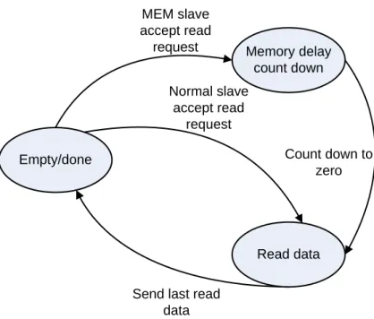
3.4.2 States of Slave Processing Transaction
Fig. 3-12 shows the states of processing transaction in slave’s read PTT. There are three states and they are empty/done, read data and memory delay count down which is used to modeling the latency when reads a memory.
A. Empty/done
The empty/done state is initial and finished state and this processing transaction is ready to accept any read request.
B. Memory delay count down
This state entered only when a MEM type slave accepted a read request. The processing transaction becomes idle and counts down several of cycles in this state. After counting down to zero, the state changes to read data state.
C. Read data
When normal type slave accepts a read request or MEM type slave counts down to zero, the processing transaction enters the read data state. In this state, slave sends read data to master until the last read data is sent. Once all data is sent, the state changes to done.
Memory delay count down Read data MEM slave accept read request Normal slave accept read request
Send last read data
Count down to zero Empty/done
Fig. 3-12 FSM of transaction in slave read PTT
Fig. 3-13 show the states of processing transaction in slave’s write PTT. There are a single loop and three states, and the states are empty/done, write data and write response.
A. Empty/done
The empty/done state is initial and finished state, and this processing transaction is ready to accept any write request.
B. Write data
When slave accept a write request, the state of processing transaction becomes write data state and slave is ready to accept write data until last write data accepted.
C. Write response
After slave accepted last write data, slave returned the write response to the master in write response state, and changed the state to done.
Chapter 4 Design of AXI Bus Interconnect
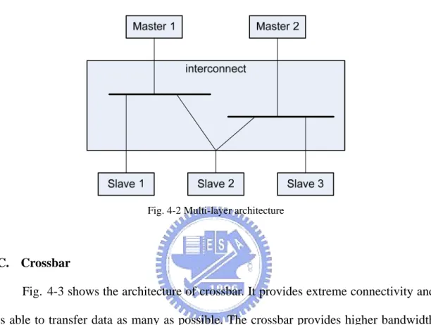
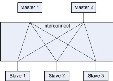
4.1 Bus Interconnect
The architecture of an AXI bus interconnect can be categorized into three, shared bus, multi-layer, and crossbar.
A. Shared Bus
Fig. 4-1 shoes the architecture of shared bus. It is low cost and easy to design. Although there is only one shared bus to transfer data, the packet-based bus (AXI) protocol which supports out-of-order transfer wouldn’t result in congestion easily. Packet-based bus protocol is more tolerable to traffic than traditional pipelined (AHB) bus under single shared bus architecture.
Fig. 4-1 Shared bus architecture
B. Multi-Layer
Fig. 4-2 shows the architecture of multi-layer. It provides more connectivity to transfer more data at the same time but need more hardware cost than shared bus. However, not all cases are able to adapt to this architecture such as that all devices
need connect each other or connectivity concentrates on single device and the other devices need little connectivity, which results in too much layer and hardware inefficient.
Fig. 4-2 Multi-layer architecture
C. Crossbar
Fig. 4-3 shows the architecture of crossbar. It provides extreme connectivity and is able to transfer data as many as possible. The crossbar provides higher bandwidth than the shared bus and the multi-layer, but costs great hardware cost. Using crossbar dose not need complex arbitration policy because the big issue is the hardware cost and bandwidth. Although the providing bandwidth of crossbar overcomes with the shared bus and the multi-layer, there is still a problem which is the same with multi-layer. When the traffic is concentrated on a single device, the hardware becomes inefficient. ARM PL300 [12] and Synopsis DesignWare AXI IIP [13] adopt the crossbar as their architecture because they only considerate the bandwidth but hardware cost.
Fig. 4-3 Crossbar architecture
The bandwidth providing from the three architectures sorting from high to low are: crossbar, multi-layer, shared bus, but sorting according to the hardware cost are: shared bus, multi-layer, crossbar. This simple summary gives us a basic guild to choose the architecture of bus interconnect. However, if we consider the bus traffic of a SOC platform, we will find the memory access is always occupied the most percentage of bus traffic [14].
According to the mentioned before, when bus traffic concentrates on single device (like memory), the bandwidth difference among the three bus interconnects would not be significant. Since the difference of bandwidth is not obvious, the hardware cost is the most important issue. Therefore, we adopt the shared bus as our architecture of interconnect.
4.2 Transfer Mode
Before describing our transfer modes, we give an assumption like the Fig. 2-8(b). We assume the READY signals of masters and slaves are always high if the master and slave are capable of accepting transfers.
According to the conclusion of chapter 2.2.2 Channel Handshaking, AXI is suitable for register input and combinational output circuit but there is a problem of inserting a layer of register slice as shown in Fig. 4-4. The inserting register slice makes the limitation of bandwidth utilization become 50 % based on ensuring there is no error occurring at the next cycle after information or data transferred. Fig. 4-5 shows the error case. There is an error transfer occurring at the cycle T3 and T4 of Fig. 4-5. Fig. 4-6 is the correct case and it makes the limitation of bandwidth utilization 50%. To increase the bandwidth utilization, we design another three transfer modes. They are interleaved mode, data lock mode and hybrid mode. Each of them is suitable for some devices and cases.
Fig. 4-5 Error case of data transfer
4.2.1 Normal
Mode
Normal mode is the basic transfer mode of the AXI. Fig. 4-7 is a example of transferring four transactions. Each transfer takes two cycles to complete the transfer. The bandwidth utilization is only 50%. Although the normal mode only has half the bandwidth utilization, all transfers fit the AXI protocol.
Fig. 4-7 Timing diagram of normal mode
4.2.2 Interleaved
Mode
We propose an interleaved transfer mode which improves the bandwidth utilization. The interleaved mode allows the two transfers from different devices to be transferred within two cycles.
Fig. 4-7 illustrates an example of using the interleaved transfer mode. Both device M0 and M1 send write address through the bus. By using the interleaved mode, M0’s request A is sent first. While request A is transferring through the bus, request C
from M1 is being processed. The one cycle latency introduced in the normal mode for request C is therefore hidden by request A sending time. As a result, the total time to send all 4 requests from M0 and M1 would only take 5 cycles, which is only 62.5% of the time taken by using the normal transfer.
The interleaved transfer mode can also be applied to data channels in the same manner. Note that the implementation of interleaved mode can be done within the bus interconnect design. There’s no need for additional hardware in device interface and bus protocol modification. However, to use the interleaved mode, the source of the transfer from each device must be different. Otherwise, the normal mode must be used.
Fig. 4-8 Timing diagram of interleaved mode
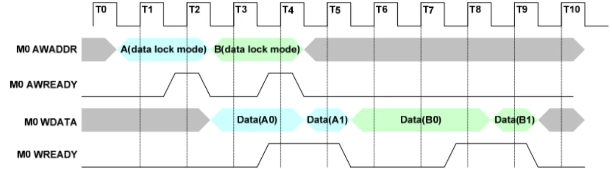
4.2.3 Data Lock Mode
For the situation of only one device accessing the bus, we design another transfer mode: data lock mode. This mode allows the devices to perform the continuously data
transfers of a transaction.
Fig. 4-9 illustrates an example of using data lock mode. Device M0 sends data lock request A and device M1 send normal request B. Once bus interconnect accepted the request A, the bus interconnect recorded the transaction’s ID of request A. When the matched ID appears in the data channel, the bus interconnect uses data lock mode to transfer the data continuously. This example transfers four beats data which takes the same time as the Fig. 4-8.
Fig. 4-9 Timing diagram of data lock mode
To acknowledge the bus interconnection which transaction uses data lock mode, we proposed three two ways to acknowledge the bus interconnect.
A. Using the signals in address channel
We uses address channel port “ARLOCK/AWLOCK” which contains the control information to acknowledge the bus interconnect that there is a data lock mode transaction. Although doing that makes a misunderstanding with the specification, if the masters and slaves are able to accept continuous data transferring, there is
influence on the system.
B. Build-in the bus interconnect
The second way to acknowledge the bus interconnect is using address decoding to distinguish between the normal transaction and data lock transaction. This implementation would not additional modify for the masters and salves. The only overhead is that the bus interconnect needs to configure which device using data lock mode in advance.
These two ways to acknowledge the bus interconnect do not conflict with each other so they could use both in the bus interconnect.
Except the acknowledgement of data lock mode, using data lock mode also needs to record the ID of transaction using data lock mode. Therefore, the bus interconnect must need addition hardware to store the ID so we design the hardware “read/write data lock buffer” to record which transactions uses the data lock mode. The read/write data lock buffer has a limitation of capacity of recording transactions so that if the read/write data lock buffer is full, those requests of transactions using data lock mode will not be accepted by bus interconnection. According the description of prior, transactions using data lock mode will block each other when the read/write data lock buffer is full. The situation of transactions blocking each other is fine in the system without memory controller because the bandwidth utilization is still high enough. In a system with memory controller, if the transactions block each other and memory controller responses data with high initial latency, the bandwidth utilization will be low. The out-of-order transaction completion allows memory controller to hold all request form transactions and give the memory controller wider scope to rearrange the transaction to reduce the latency and power consumption [10]. To make the memory controller keep the most scope of rearranging transactions, we can increase the read/write data lock buffer but it need more hardware cost. Therefore, we
designed another transfer mode to deal with the transactions using data lock mode and increase the scope of memory controller. This mode is described in later section.
Although data lock mode provides continuously data transferring, if all transactions use data lock mode to transfer data, the bandwidth utilization would result in a limitation. Fig. 4-10 shows the reason. The first data lock transaction is nothing special but the second data transaction needs an additional cycle to start transferring data. At cycle T6, the bus interconnect ignores the request of device M0 for ensuring that there is no error case like Fig. 4-5 occurred and then the bus interconnect processes the request of device M0 at cycle T7. After the bus interconnect processed the request of device M0, the bus interconnect started data lock mode transferring. When the two data lock mode transactions come from the same source, the bandwidth utilization would reach the limitation. There is a formula to calculate the limitation according to the burst length. Table 4-1 shows the bandwidth utilization with corresponding burst length.
% 100 _ 2 _ _ × + = length burst length burst n Utilizatio Bus
Table 4-1 Limitation of bandwidth utilization using data lock mode Burst length Provide bandwidth utilization
2 50.00% 4 66.67% 6 75.00% 8 80.00% 10 83.33% 12 85.57% 14 87.50% 16 88.89%
4.2.4 Hybrid
Mode
Hybrid mode is used to increase the scope of memory controller to rearrange the transactions. Fig. 4-11 shows the flow of hybrid mode. When the read/write data lock buffer is full, the bus interconnect treat the transaction as a normal transaction according to the hybrid mode counter. If the counter does not reach the threshold, the bus interconnect treats the data lock transaction as a normal transaction. Once the counter reached the threshold, the data lock transaction would not treat as normal transaction until the counter reset. When the bus interconnect complete a data lock mode transaction, the counter would rest.
If we treat all transactions as normal transactions when data lock buffer is full, the ratio of normal transactions and data lock mode transactions would become to the result we not expected. This may make the interleaved mode can not be applied because the data lock mode is always applied to the device required mass bandwidth. Therefore, we set a threshold to hybrid mode counter to prevent the case occurred.
Fig. 4-11 Flow of hybrid mode
4.3 Arbitration Policy
4.3.1 Our AXI Arbitration Flow
The AXI protocol is defined in transfer level not transaction level. Therefore, the normal mode and interleaved mode in address channels and data channels also perform in the transfer level. Only the data lock mode in data channels is in the transaction level so we arbitrate the request of transactions in the transfer level.
Fig. 4-12 shows our AXI arbitration flow. The principle of our arbitration is to grant based on which transfer mode is being used, namely the data lock mode and the normal mode. First, we check if there is any other transaction already using the data lock mode. If data lock mode is already in use, arbitration is done. Second, we check if the data lock mode buffer is full or not. If buffer is not full, we check if there is necessary to arbitrate the data lock mode transactions. If the buffer is full, we directly check if there is necessary to arbitrate normal mode transaction. We arbitrate the data
lock mode transaction first and then arbitrate the normal mode transaction. This is because of that the data lock mode transaction always comes from high priority device or mass bandwidth required device. Arbitrating the data lock mode transaction first is like giving more priority to the device using data lock mode so doing this helps us to configure the priority properly.
Fig. 4-12 Flow of our arbitration
4.3.2 Fixed
Priority
Fixed priority uses a pre-defined priority order of devices to arbitrate which device has the right to access the bus interconnect while the contention occurs. The advantages of fixed priority are low hardware cost and easy to implement. The
drawbacks of fixed priority are that fixed priority will result in starvation on low priority devices and cause some transactions extreme latency.
4.3.3 TDMA
Fig. 4-13 illustrates the TDMA policy. The TDMA divides time to very many time slots and distributes the time slots to devices according to bandwidth requirement. Each device has its own amount of time slots. When a device becomes the highest priority device, the number of its available time slot starts to decrease. Once the number of available time slot becomes zero, the priority of the device becomes the lowest and the priority of the second device becomes the highest. The darkened squares in Fig. 4-13 means that the master are granted.
The advantages of TDMA are:
z Predictable bandwidth allocation according to distribution of time slots z Predictable latency
z No starvation problem The drawbacks of TDMA are: z Ignoring the urgent devices
Fig. 4-13 Illustration of TDMA policy
4.3.4 Round-Robin
Fig. 4-14 illustrates of Round-Robin policy. Round-Robin divides the clock cycles to an arbitration cycle. The darkened squares in Fig. 4-14 mean that the masters are granted. Each device has its own threshold which is pre-defined according to the bandwidth requirements. As the device is granted, its counter adds one. When the counter reaches the threshold, the priority of the device becomes the lowest wherever its previous priority is in any place. Taking the master 1 as an example, the threshold of master 1 is two. After master 1 was granted twice, the priority of master 1 became the lowest.
The advantages of Round-Robin are:
z Predictable bandwidth allocation according to devices’ threshold z Predictable latency
z No starvation problem
z More complex control than TDMA
z More hardware cost than fixed priority and TDMA
Master1 Master2 Master3 Master4 Master5 Master2 Master3 Master4 Master5 Master1 Master2 Master4 Master5 Master1 Master3 Master4 Master5 Master1 Master3 Master2 Master4 Master5 Master3 Master2 Master1 Time Master1 Master2 Master3 Master4 Master5 Master4 Master5 Master1 Master3 Master2
Fig. 4-14 Illustration of Round-Robin policy
4.3.5 Lottery
The lottery policy is a probability based arbitration policy. There is a ticket manager which is like an arbiter to decide which device is the winner. Each device has its own amount of tickets according to the bandwidth requirements. When the devices want to access the bus, they send the request to the ticket manager. The ticket manager knows how many tickets each device has and then sums the tickets from devices that want to access the bus. After summing the tickets, the ticket manager randomly generates a number under the sum. The ticket manager picks up the winner according to the winner’s ticket falling into which area of the device. Fig. 4-15illustrates an example. The master 1, 2 and 4 send request to ticket manager for accessing the bus. The ticket manager sums the tickets of master requested and then
generate a winner’s ticket. The winner’s ticket is 10 and falls into the area of master 4 so master 4 is granted.
The advantages of Lottery are:
z Good bandwidth allocation according to devices’ ticket z Low hardware cost
z No starvation problem The drawbacks of Lottery are: z Unpredictable latency
z More critical path than other arbitration policies
Chapter 5 Simulation and Analysis
5.1 Introduction
In this chapter, we evaluate the performance of AXI interconnect with various parameter and transfer mode settings. These parameters and settings include wrapper buffer size, configuration of arbitration policies, and transfer mode setting. We built a portable media player (PMP) platform with a video phone scenario are used to determine the impact of the parameters and settings. The reason for selecting the PMP platform is because it is a multicore platform with various tasks running the video phone scenario. Running simulation in such complex platform with realistic video phone scenario would enable the experiment result and conclusion be more suitable to real systems and applications. In addition to the AXI PMP platform, an AHB PMP is also implemented using CoWare’s AHB TLM model. However, the architecture of interconnection in AHB PMP platform is different from PMP of AXI protocol because of performance concerning. This experiment compares the performance of AXI and AHB interconnect. The result and conclusion may serve as a reference for system designer in choosing the proper bus architecture and protocol.
5.2 PMP Platform
5.2.1 Overview
Fig. 5-1 AXI PMP platform
Fig. 5-1 illustrates the system block diagram of the AXI PMP platform. The platform includes a MPU, a DSP, a video encoder, a DMA controller, a vector interrupt controller, a memory controller, a communication device, and audio/video input/output peripherals. All the devices are connected with the shared bus AXI bus interconnection. From the bus interconnect’s point of view, the platform consists of 5 master ports and 11 slave ports. The master ports include 2 regular type ports, 2 DMAC type ports, and 1 MPU type port. The slave ports have 9 regulartype ports and 2 memory type ports. Detailed device settings are shown in Table 5-1 and Table 5-2. Note that device IRQs are directly connected to the MPU, bypassing the VIC. Although this is different from real system implementation, it is equivalent to connecting the IRQ to MPU through the VIC. Only a few transactions are lost which