Test Time Reduct ion for Scan-Designed Circuits
by Sliding Compatibility t
Jau-Shien Chang
C hen-
S hang Lin
Department
of
Electrical Engineering
National Taiwan University
Taipei, Taiwan, R.O.C.
Abstract
A post generation method for test time reduction of
scan-designed circuits is developed in this paper. Maximum overlopping condition between consecutive applied patterns is identified. The application of the condition facilitated with the developed active &ding compatibility process sig- nificantly reduces the number of test clocks. It is demon- strated that the test clocks can be r e d u d by 50% on av- erage from given test sets. Further evaluation shows that,
for parity-scan, the test clocks required by our developed method are only 41% of those in [3].
1
Introduction
To increase the fault coverage and the test quality of sequential circuits, the now popular scan d e s i p had been proposed 121. The main feature of scan design is that, by a- lem is transformed into the much simpler combinational one, thereby the desirable test quality can be achieved. However, the necessity to shift test patterns and respons
es in the long scan chain may incur significant increase in test application time as well as test cost. To minimize the additional testing time while retaining test quality of scan design, various scan clock reduction methods have been proposed[l-5 ,7J
.
These prevlous works of test time reduction for scan- designed circuits can be divided into the following two general approaches: reduction during test generation or
after teat generation. To reduce the test application time during test generation, one way is to generate a combi- national test set as compact as possible. Several effective techniques have been developed to generate such compact- ed test sets[6,8-91. However, as pointed out in [3], test compaction alone is not enough to reduce test apphcation time because further reductions can always be obtained by carefully rearranging the test patterns. Alternative- ly, in [4,7], the test generation is made to switch between scan-mode and nonscan-mode, and the scan mode is used only to achieve the required fault coverage. However, for circuits with many sequential hard-to-detected faults, the scan operations w i l l occur k e uently and result in test time worse than that of full-scan[q. Moreover, complicated se-
quential test generation is involved in the process with the consequence of prolonged generation time.
re- ducing scan requirements fiom a given test set. In b,2], based on the assumption that scan-in and scan-out flip- flops are disjoint, each of the scan-in patterns is divided into several segments first. Then, the application of a test pattern to the CUT is invoked after scanning in only a segment but not necessarily a complete pattern. Thus, some faults originally detected by the later patterns may canning t
6
e flip-flops, the complicated sequential test prob-The post generation approach is characterized b
tThis work was supported in part by the National Science Council under contract number NSC-850404E002-055
become detectable by these segmented patterns and the test time can be reduced due to attern removal. More elaborate pattern-overlapping tec&uques have also been developed in 7 . The overlappin of successive pattern-
s are obtained
&
precisely controfmg the scan operation through the utilisation of don’t-care bits in the scanned flip-flops. However, for a given test set with few don’t- care bits, the overlapping often collapses due to the minor difference between successive patterns. In summary, the effectiveness of these previous works is heavily restricted by the characteristics of the given test set.Recent1 a novel idea, parityscon design, has been pro- posed in [3f in which an extra parity output is introduced to the scanned flip-flops to enhance the observability. With this simple parity output, the scan operation can be elim- inated if the fault dfects can be easily observed and the content of flip-flops can be reused. To exploit the enhanced facility, direct test time reduction has been considered in [3] by generating a pattern with part of the previous pat- tern as the constraint so that a test set with highl over- lapping patterns can be obtained. As shown in
81,
the test time is reduced by 30% on average with the modified FAN[ll]. However, the high overlapping among patterns is obtained at the expense of a much larger test set and asa result, even with the parity output, the reduction in test time ia often inferior to that by compacting the test set for pure scan design. From the observations on these previous works, it can be seen that, in order to obtain consistently good results in test application time reduction, post gen- eration approach with a compact test set is preferable.
We are going to show in this paper that more signifi- cant reduction of test clocks in scan-designed circuits can be achieved by the post generation approach. Namely, the reduction is performed after an initial test set is generat- ed. We identify the condition which d o w s the maximum overlapping between successive applied patterns and then actively modify these patterns to exploit the overlopping without sacrificin fault coverage. The experimental re-
sults on 22 ISCA%89 benchmark circuits show that, for the test sets generated by PODEM, 50% test clocks in pure full-scan can be reduced on average. Furthermore, for the parity-scan design proposed in [3], o w method needs only
52% test clock cycles of those generated in [3]. When the ven test set is aheady compact, the improvement over
i!
31 is even more sipificant, only 41% test clocks are re- quired. The reduction is achieved strictly on the domain of combinational circuit.The paper is organised as follow. Some notations and definitions about scan design are introduced in Section 2. The proposed Maximum Overlapping condition is d o scribed in Section 3. In Section 4, the active operation of slidin compatibility for maximum overlapping is intro- duced. gection 5 provides the Experimental Results. The Conclusions are given in the last Section.
1 2
-
-
I *D
I I-
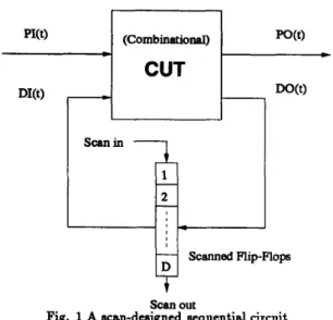
scan outFig. 1 A scan-designed sequential circuit scannedplip-Flop
2
Scan Design
In this section, the full scan-designed circuits w i l l be briefly discussed. Some notations and definitions useful for subsequent discussions will ale0 be introduced.
For a scan-desyed circuit as shown in Fig. 1, each test pattern t for t e CUT (Circuit Under Test) consists of two parts: the part applied to PI denoted as P I ( t ) and the other part for the FFs (Flip-Flops) as D I ( t ) .
In
the test application o f t , D l ( t ) must first be shifted into the scan path which generally consists of all FFs in the circuit. LetRESP(t)
be the response of CUT after applying t.R E S P ( t )
can be similarly divided into P O ( t ) andDO(t),
where PO(t)i
the response appearing at PO and DO(t) is that to be loaded into FFs. DO(t) must also be shitted out of the scan path for observation, which may overlap with the scan-in of the n u t pattern.Let
T
be the test set to be applied and D be the number of shifts for each pattern (in general, D is the number of scanned flip-flops), then total testing time, &, iswhere S and C are the periods of a shifting clock and sys-
tem clock, respectively. Assuming S =
C,
t~ becomesTTC, is then tT = ( I T
I
+ I ) *D *
S+ ITI
*C t T=
((I
TI
+1)*
D+I
TI)
*
STTC
=
(ITI
+ 1 ) * D+I
TI
(2.1) (2.2) (2.3) The total test clocks ofT
for a scan-designed circuit,From (2.3), it can be seen that, to reduce the total test clocks, we can either compact the test set
T
as small as possible or shorten the number of shifts for each pattern. For test set compaction, there ahead exist effective tools such as COMPACTEST[Q] and TSRb]. At preeent, TSR has been adopted in our work. Therefore, in this paper, we will aim at how to reduce the number of test clocks onD . Note that we assume the scan-chain topology has been determined before test clock reduction.
3
Maximum Overlapping
Given a test set, the primary step of test clock reduction is to identify the maximum overlapping possible between twoconsecutive patterns without sacrificing fault coverage. In thie section, the condition for Maximum Overlapping w i l l be diecussed.
Since the purpose of reduction is to use the current con- tent of FFs as part of the next scan-in pattern, two types of overlapping are possible, either overlapping with the response of the previous pattern or the previous pattern i t d . Both need some elaboration. In the first case, one must be sure that the content of FFs is not contaminated by the fault dfect of all possible faults under consider& tion. And in the second case, the fault dfect should be observed directly from primary outputs and the FFs re- tain the previous pattern by skipping the load response operation.
have been proposed in [3]. Under the constraint that all &e activated faults of the current applied pattern t; can be observed at POs, the following two cases are accepted for reducing the test clocks of the next pattern t;+l.
case (a) Complete DO-rewe. DO(t;)
case (b) Complete DI-rewe: D I ( t ; ) E DI(t;+x). The
'
3' above is the computible relation. Two vec- tors are said to be compatible if all the corresponding bits are either of the same logic value or one of them is '2'(don't care). For example, the two vectors, u l = (0201) and s2
=
(010~)~ are compatible and denoted as ul EE u2.When one of the above two cases is satisfied, the current content of FFs can be completely reused as part of &+I and the scan-in operation of t;+l can be eliminated. However, the conditions used in [3] are clearly restrictive. The gen- eral conditione for "mum overlapping will be described next.
To allow maximum overlapping, we w i l l first examine the conditions by which the content of FFs can be safely reused.
As
discussed in the beginning of this section, to reuse the DO-part, one must be sure that no fault effect w i l l appear ip FFs.In
other words, the content of FFs must be the fault-fiee response to allow safely resue. This is by no means trivial since the fault effect of some faults can only be observed after scanning out the content of FFs. Nevertheless, we generally need not scan out the whole chain to determine whether or not it is the fault- free response. This is stated in the following observation. Observation 1 (DO-Reuse): Under single fault as- sumption, after a pl ' g a pattem t to the CUT and load-ing its response $ O r i n t o the scanned FFs, the presence of a detectable fault o f t can be determined fiom either POs or its firat fault effect bit in DO t). Furthermore, if t in DO(t) have been observed to be fault-he, then these faults are notpresent and D O ( t ) is the fault-free response.
The implication of Observation 1 is that after examin- ing a few possible fault-effect bits in DO(t
,
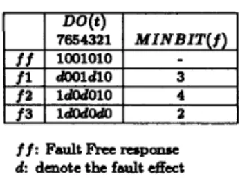
the remain- with the next pattern. From the observation, the num- ber of bits to be shifted out after applyin a pattern is then M A X ( M I N B I T ( f ) ) for each detectafde fault f by the pattern. This number can be easily determined by the fault simulation bdore actual test application. After shiftin out this predetermined number of bits, it can be decide! whether or not the remaining bits are fault-free and can be safely reused. For the example shown in Table 1, suppose three faults {fl, f2, f3) are detected by apply- ing pattern t and the fault-free DO(t) = (lOOlOlO), by means of possible fault-effect bits computation in DO(t), the faulty bit nearest to the scan-out pin is selected as M I N B I T ( f ) . Since the maximum ofMINBIT
is found to be 4, D O ( t ) must be shifted out 4 bits before re-usage.Two special casea for pattern overlappin
DI(t;+l),
POs and the first fault effect bits of al
I
detectable faults ofI
I
DO(t)I
1
Step Init 1 a 3 7654321 MINBIT f f f 1001010 f l dOOld10f a
ldOdol0 f 3 1dodmDI(t) 654321 Operation DI(tl)? tl 101Ooo
t 2 010011 No
t 3 111110 No
tl 101Ooo
t 2 zlzOl0 bit raising No
t 3 1~1110 bit raising No tl zlOl00 &ft out 1 bit
t2 OlOzzl bit raising No
t 3 11~110 bitraising No
tl zzlOl0 ahiftout 2 bib t 2 01~011 bit raising No
t 3 111~10 bit raising YCS
f f : Fault
Free
rerpcaw d denote the fault &atTable 1. Example of MAX(MINBIT(f)) Computation
The DI-reuse condition is the same as described earlier and formally given as follows.
Observation 2 (DI-Reuse): The c w e n t pattern m the FFs, DI(ti
,
may be part of D I ( t , 1) only if all the detect-ed faults o)ti can be obserued at
$Os
alone.It can be s e n that when fhult dfects must be observed from FFs, the DI-reuse can not be applied. The problem can be significantly alleviated if extra hardware is used to enhance observability such as that in parity-scan designed condi- tions to reuse the current content of FFs. The &lowing observation provides a sdicient condition for overlapping the next pattern with the current content of FFs, BO that the test clocks can be reduced.
Observation 3 (Maximum Overlapping): The cur- rent content of FFs, S F F ( t ; ) ( D I ( t i ) M DO(ti)), may constitute part of D I ( t i + l ) without sacrificing fault cwer- age if the conditions of Observations 1 or d are satisfied respectively.
The last condition of Observation 3 requires only the trailing part of SFF(ti) is compatible with the leading part of D I ( t i + l ) without explicitly specifying the size of parts. The condition is named sliding compatibility of S F F ( t i ) and DIlti+l). Sliding compatibility is the generalisation of comp ete compatibdity for test clock reduction.
The extent of overlapping which can be actually achieved from the above observation depends on the order- ing of scan chain. Although it is theoretically possible to rearrange scan path to obtain maximum reduction, phys- ical constraints discourage such arbitrary rearrangement. Hence the aspect of rearrangement is not discussed and, in our experiment, the natural ordering of scan path is used. Based on Observation 3, the process for maximum over- lapping can be performed as follow. In the previous ex- ample in Table 1, after shifting 4 bits out of DO(t) =
(lOOlOlO), there are still 3 bits can be overlapped with the next pattern. In other words, three scan clocks can be re- duced if the next pattern is compatible with (zzzz100).
To take fullest advantage of this situation, the next pat- tern can be chosen accordingly. When this is not possible, the next choice can be the one that is sliding compatible with (zzzzlOO), i.e., compatible with (zzzzz10) and then with (zzzzzzl). Note that, with sliding compatibility, the extent of test clock reduction decreases step by step. In the extreme case, not even sliding compatibility is possible and regular scan operation must be performed. A more dfective implementation of this process will be described in the next section.
drcuits[3].
The above two observations are the necessar
4
Active Sliding Compatibility
The goal of maximum overlapping is to optimally reuse the current content of scanned FFs in the next scan-in operation. However, for a test net lack of eliding compat- ibility between patterns, the reduction on test clock w i l l not be sienificapt. It means that the dfectiveness of max- imum overlap could be restricted by the nature of the given test set.?%"e, to fnrther enhance the reuse in maximum overla ping, we pro- the process, Active S-
liding Compatib&, which actively modifies the test set for sliding compatibility and increase the chance of reuse while keeping the overall fault coverage intact.
The basic idea of active &ding compatibility is to take advantage of the over-specification property of the given test set. For example, for a pattern t
=
(01111) in a test setTI
the fault coverage ofT
may still keep intact when t is changed to t' = (0~121). In this case, t is said to be over- speCijiedin T and these bits changed from '0' or '1' to '2'are said to be raised Comparing t with t', t' obviously has more chances to be compatible with any arbitrary vector than t . Thus, when trying to reuse the current contents of FFs for the scan-in o f t , mo-g t to t' would be a better choice.
In active sliding compatibility, for the next pattern to be scanned in, those sliding incompatible bits with the current contents of FFs will be moditied (raised) to '2'
for re-usage. However, during raising these incompatible bits, it is essential to preserve the overall fault coverage, DE!7'
TI
F ) . The following observation allows us to per- intact[6]. Ddine BSST(t, F ) , the essential faults of t , asthe set of faults in F that can only be detected by t but not others in
T.
Observation 4: Given a fault set
F
and a test set T ofF,
for a pattern tE
T,
if t is substituted by t'
such thatform t
6
e raising operation while keeping the f d t coverageThe implication of Observation 4 is that active sliding compatibility can be performed by raking some bits of t while monitoring the detectability of ESST(t,F). And, the detectability of ESST(t, F ) can easily verified by fault simulation.
I
I
I
ContmfrI
I
Table 2. Example of active compatibility
With Observation 4, the brief procedure for maximum overlapping described at the last of Section 3 can be re- fined to the active sliding compatibili process for achiev- trated by the following example. As shown in Table 2, for ing more reductions on test clocks.
?i
he process is illus-a test set
T
=
(t1,
t a l t s } , after applying t1,
active slid- ing compatibility is performed to select the next applied pattern. Only DI-rerw is considered in this example for ally incompatible. In step 1, after the riusing operabon on these incompatible bits, the DI-parts of the three patterns are still incompatible. Therefore, one hift out o eration is performed on DI(t1). In step 2, after the DI(t1ris shifted out 1 bit, active operations for compstibht U performedon
D l ( t a )
and Dl(t3) again. Unfortun~t&, itale0
fail- s. In step 3, after the content of DI(t1) is shifted out one more bit, the DI-parts of tl and ts become compatible after raising. Thus, 4 scan docks can be saved for the scan-in of ts. Without these active raining operations, only one scan clock (choosingta
as the next pattern) can be reduced in this example.eimplicity. Initially, DI(tl), D l ( t 2 ) and .Dl(ts) I L ~ mutu-
5
Experimental Results
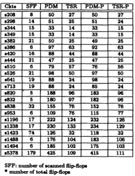
To show the effectiveness of our method (ACT), these test clock reduction techniques proposed in t b paper have been implemented on SUNCSPARC2 workstation and 22 ISCAS’89 benchmark circuits arc evaluated.
[ Ckts
I
SFF
I
PDMI
TSRI
PDM-PI
T S R PI
SFF: number of ~~c(LaDed fipflopa number of totd fipflop.
Table 3. Test sets of W A S 8 9 benchmark drcuitB In Table 3, the number of Scanned Flip-Flops (SFF) of these circuits are shown. In addition, two initial test sets of these circuits are evaluated for both hll-scan and parity- scan version. One initial test set is generated by a simple PODEM-like ATPG and the other is its hi hly compacted set by TSR[6]. These two test sets can %e regarded as two extremes for an arbitrarily given test set. The sises of these four different test sets, two for full scan and two for panty-scan 3 are also included in Table 3. For the test sets in PDl&-!b and TSR-P columns, they are generated in
a similar way to PDM and TSR test sets except a parity- checking path for pseudo POs (i.e. scanned FFs) and an extra PARITY output are added during test eneration.
In
Table 4 and 5, the test clock reduction res& of ACTon the PDM, TSR, PDM-PI TSR-P test Bets are shown.
The comparison of ACT with previous works are provided in Table 6.
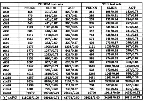
In
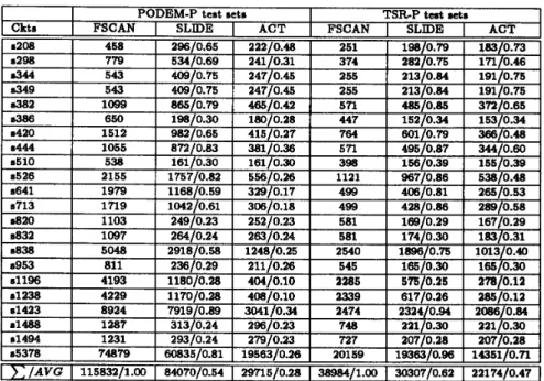
Table 4, the test clocks generated by ACT for PO- DEM and TSR test sets are ven. The final results are shown in the ACT column anfthose only with sliding but without bit-raising operations are listed in the SLIDE col- umn. The number &er each datum is the normalised ratio with respect to pure full scan (FSCAN) of the given test set. For the PODEM test sets, by the sliding operation (SLIDE), 29% test clock reduction can be achieved on av- erage as shown in the last row. It can be seen that SLIDE is more effective for those circuits with leas scanned flip-flops such M s820, s832, e1488 and s1494. For those circuits with a large amount of scanned FFs such as s1494 and135378, the reduction is less successful due to the difliculty of overlappixy between successive scanned patterns. How- ever when bitraising is added to incream the chance of overiapping, M shown in the ACT column, up to 46% and
65% reduction on test clocks for s1423 and (15378 can be obtained respectively. This shows the dfectiveness of the
r o p d d v e sliding compatibility process. O n avera e, gy ACT, 50% of test clocks for FSCAN can be reduced. $01
the TSR test sets, althou h the test Bets are much more compact than those of PbDEM and hence there is less chance for overlapping, 27% reduction can still be achieved by our methods. When comparing the total test clocks of FSCAN for
TSR
test sets with those for PODEM test set- s in the x / A V G row, leas than 1/3 (38268/118036) of the test clocks are required, a very sienificant reductionon test clocks and test cost. It demonstrates that using a
compact test set M the starting point of test clock reduc- tion is worthwhile and the efforts on the additional test set compaction can be well-justified.
For the arity-scan desi ned circuits, the results of A C
T
on P0DIki-P and TSR-5 test sets are shown in Table 5.In
comparison with Table 4, with the extra parity out ut, the aver e reduction ratio can be increased from SO& to72% foryODEM test Bets and from 27% to 53% for T-
SR
test sets.This
shows the positive &ect of enhanced observability by the parity output. Note that, for these circuits with more scanned FFs such as 8838, s1423 and~ 5 3 7 8 , the results of ACT on TSR and TSR-P test sets are quite close ((1163,1013
,
(2285,2086), (14252,14351)). The and compacted test sets, the fault effect of each fault in these circuits are more likely to reach many FFs and scan operations for each pattern generally can not be avoided. However, &om Observation 1, we are able to observe the existenceof
these faults through a few shift-out operations almost M dfedive as adding an extra parity output. Itsuggests that, in those circuits with lar e number of flip
flops, it is more advantageous to use t f e proposed ACT startin from the compacted test set since it can accom- plish &ost the same amount of test clock reduction as the additional parity chain, albeit without any hardware overhead.
The comparison of ACTwith the previous work, Panty- Scan 31, is shown in Table 6. The test clodre by [3] are parity output are shown in the ACT-PDM(P) and ACT- TS P ) column respectively, which are identical to Table with respect to PSCAN. Comparing ACT-PDM(P) and PSCAN, except a1196 and ~ 1 2 3 8 , our results are far sup* nor to those of [3]. O n average, the test clodre of ACT- PDM(P) are only 52% of those of PSCAN. It clearly shows effectiveness of the p r o p d active test clock reduction.
In
particular, for e1423 and ~ 5 3 7 8 , 61% and 75% reduction can be achieved, even though the test set Bise used in [3]are approximately equal to that of the PODEM-P test set shown in ‘Igble 3. The result demonstrates the merit of reason is as follows.
I)
ne to with a large number of FFslist
c l
in the PSCAN column. The results of ACT with theFSCAN: test do& of pure Full Scan
SLIDE ACT without bit-raining
ACT: Active Sliding Compatibility technique
Table 4. h u l t s of kat clock reduction by ACT
post generation approach of test clock reduction. It is al-
so interesting to compare PSCAN with ACT-TSR(P). In each evaluated case, the result of ACT-TSR(P is far bet- is only 41%. Recall that, in [3], the test sets are generated by preserving as more common arts as possible among patterns to increase the chance o f overlapping. Evidently, the compactness of the enerated test set is scarified. This comparison result clearfy shows that scarifjkg the com- pactness of the test set for overlapping is not worthwhile and a compact test set is desired for test clock reduction in scanned design.
In the last column of Table 6, the CPU-time for ACT- PDM(P) is shown. Except ~5378, all the examples can be completed in one minute. For ~5378, due to its circuit she, lar e test set and scanned FFs, more CPU-time, albeit not pr Lbitively long, is required. For ACT-TSR(P), becauee the test sets are much more compact than those of ACT- PDM(P), the CPU-time is far less than that shown in the Table. For example, in ACT-TSR(P), the CPU-time for e5378 is only 448 seconds.
ter than that of PSCAN. The average ratio o
1
test clocks6 Conclusions
Test time reduction for scan-designed circuits has been investigated in this paper. To reduce the lengthy shiftin operations in the long scan path, post generation metho!
to optimally reuse the contents of the scanned flip-flops have been developed. From the experimental results on 22
ISCAS89 benchmark circuits, up to 50% test cloclrs can be reduced on average by the proposed method. Furthermore, when the parity output is included in the scan-designed CUT, the resultant test clocks by ACT have been only 41% of those in [3]. It has been reported that by switching be-
tween scan-mode and nonscan- mode, further reduction on test clock cycles are possible in pure scan designed circuits. However, a sequential circuit test generation w i l l then be required and the test generation time will be substantially increased. To retain the advantage of simple combina- tional test generation of scan-designed circuits, the mode- switching is not perkxmed in this work.
References
[l]
M.
S.
A b d i andM.
A. Breuer, "Scan P a t h With Look AheadShiftin
(SPLASH)," Proceedingsof
1986 International %st Conference, pp.
696-704.
Sliding Parity Reaponse Compaction %roceer& ings of 1987 International Test Conjerence, pp.[3]
H. Fujiwara and A. Yamamoto, "Parity-Scan De- sign to Reduce the Cost ofTest
Application," IEEE !bzna. Computer Aided Design, Vol.12,
No.10,
pp.1604-1611,
Oct.1993.
[4]
S.
Y. Lee andK. K.
Saluja, "An A orithm t o[2]
M.
S.
Abadir, "Efficient Scan Path TestinUsin
332-335.
Reduce
Test
Application T i m e in Fu4i
Scan De- eigne," Proceedingsof
1992 ICCAD, pp.17-20.
[5]
I.
Pomeransand
S.
M.
Reddy, "A Test Appli-cation Scheme for Embednded
Full-Scan
Circuits t o Reduce Testing Coats, Proceedingsof
First Asian Test Symposium, pp.206-211,
1992.
[
);/AVGI
11583211.00I
8407010.54I
2971510.28I
3898411.00I
3030710.62I
2217410.471
Table 5. Results of teat clock reduction by ACT with PARITY output[6]
J. S.
Chang and C.S.
Lin, "Test Set Compaction for Combinational Circuits," Proceedingsof
First Asian Test Symposium, pp.20-25,
1992.
[7]
W. C.
Lai,
C. P. Kung and C.S.
Lin, T e s t TimeReduction in Scan Design Circuits," Proceedings
of 1993 EDAC, pp.
489-498.
[8]
Gert-Jan Tromp, "Minimal Test Sets for Combi- national Circuits," Proceedings of 1991 Intema- tional Test Conference, pp.204-209,
1991.
[9]
1.
Pomeranz,L.
N.
Reddy and Sudhakar M. Red-dy, "COMPACTEST: A Method t o Generate Compact Test Sets for Combinational Circuits," Proceedings of 1991 International Test Confer- ence, pp.
194203.
[lo]
P.
Goel, "An Implicit Enumeration Algorithm to Generate Tests for Combinational Logic Circuit- s," IEEEThana.
on Computers, Vol. C-30, No. 3,Mar. 1981.
[ll]
H.
Fujiwara andT.
Shimono,
"On
the accelera- tion ofTest
Generation Algorithms," IEEE !&an- d . Computers, Vol.C32,
No.
12,
pp.1137-1144,
Dec.1983.
[12]
E.B.
Einchelberger andT.
W.
W i l l i i ,
"A logic design structure for LSI testability," Proceedingof Design Automation Conference,
1977,
pp.462-
468.
I
I
ACT- I ACT- I1
I
CktaI
PSCAN[3]I
PDM(P)I
TSR(P)I
TIMEI
1.208 I 279 I a22/0.80 I 18310.66 I 2.0I
I8298 I 495i
24110.49i
1n10.35i
3.0I
24710.54 191 0.41 24710.56 191 0.43 46510.56 37210.45 a386 380 180 0.47 153 0.40 8420 1296 415 0.32 366 0.28 7.0 8444 936 38110.41 344 0.37 5 .O 8510I
354I
161/0.45I
15510.44I
6.0 8526 I 1707 I 10.0>;
101709 29504 22009 AVG 1 .o 0.52 0.41ACT-PDM(P): nrulta of ACT on PDM-P tat a& ACT-TSR(P): nrulta of ACT on TSRP teat d m