Large coherent acoustic-phonon oscillation observed in InGaN/GaN
multiple-quantum wells
Chi-Kuang Suna)and Jian-Chin Liang
Department of Electrical Engineering and Institute of Electro-Optical Engineering, National Taiwan University, Taipei 10617, Taiwan, Republic of China
Christopher J. Stanton
Department of Physics, University of Florida, Gainesville, Florida 32611 Amber Abare, Larry Coldren, and Steven P. DenBaars
Department of Electrical and Computer Engineering, University of California, Santa Barbara, California 93106
共Received 9 March 1999; accepted for publication 2 July 1999兲
We have observed coherent acoustic-phonon oscillation in InGaN/GaN multiple-quantum wells. With femtosecond pulse excitation, photogenerated carriers screen out the strained-induced piezoelectric field and initiate the coherent acoustic-phonon oscillation. The resulted modulation of the piezoelectric field will then cause large optical property oscillation through the quantum-confined Stark effect. © 1999 American Institute of Physics.关S0003-6951共99兲01335-2兴
Progress in femtosecond lasers and ultrafast spectros-copy technology has enabled us to generate and directly ob-serve the coherent oscillation of phonon modes.1–7 Oscilla-tion changes in optical properties have been observed in GaAs,1,2Ge,3and a number of other materials.4,5In semicon-ductors, carriers can be excited by ultrashort pump pulses in a spatial area much larger than 1 lattice unit cell and the excited carrier populations 共with wave vector q⬵0) are coupled to the corresponding optical-phonon modes 共also with q⬵0).6Besides being incoherently populated, some of these optical phonon modes can behave like classical oscil-lators and have nonzero time-dependent displacement. This is different from spontaneous emission of phonons, which is an incoherent process that populates the phonon modes with the expectation value of each mode being zero. The corre-sponding modulation of the material dielectric constant, due to coherent oscillation of optical phonons, could then be ob-served by changes in the intensities of transmitted or re-flected probe light pulses.
For acoustic phonons, it is much harder to selectively excite a specific acoustic phonon mode by q⬵0 carriers in bulk materials. With the aid of laser-induced grating tech-niques, coherent acoustic waves of a few MHz to 30 GHz can be induced through periodic optical fields, photothermal gratings, or the photon-excited periodic carrier distribution, all with nonzero corresponding wave vectors.8,9Similar tech-niques can be applied to high-frequency acoustic wave gen-eration by using a multilayer structure10 or a repeated nanostructure,11where larger wave vectors can be achieved. With the acoustic wave reflection on the boundary of a thin fine structure, optical reflection oscillations corresponding to the round-trip time have also been previously observed12and coherent acoustic-phonon oscillations corresponding to spherical acoustic modes in quantum dots were also
reported.7 Semiconductor superlattices exhibit zone folding of the acoustic branches within the mini-Brillouin zone due to the artificial periodicity, also enabling the observation of coherent oscillation of the zone-folded acoustic phonons in AlAs/GaAs superlattices.13,14However, the observed reflec-tion modulareflec-tion ⌬R/R is extremely small, on the order of 10⫺5, such that a step-and-repeat detection scheme with a fast scanning time delay is required to maintain a signal-to-noise ratio of better than 10⫺6 in femtosecond pump-and-probe systems.14The coherent phonon excitation is probably due to photoexcited carriers-induced stress in the well layers,13 and the detection is based on refractive index changes caused by acoustic deformation potential–exciton coupling.14
In this letter, we demonstrate that in multiple-quantum wells共MQWs兲 with strain-induced piezoelectric-field, strong coherent acoustic-phonon oscillation can be easily generated and the large modulated absorption in probed pulses with ⌬T/T on the order of 10⫺2 can thus be observed. The
oscil-lation frequency can be tuned by changing the period width of the multiple-quantum wells.
The experiments were performed at room temperature on 14 periods of InGaN/GaN MQWs. The recent demonstra-tion of high-brightness light-emitting and laser diodes with InGaN MQWs as active regions15has established the III–V nitrides as key materials for optoelectronics operating in the green-UV wavelength range. Because of the large piezoelec-tric constants along the 关0001兴 orientation in group III ni-trides, a high strain-induced piezoelectric field is expected 共on the order of MV/cm兲 and would play an important role in the optical properties of 共0001兲-oriented InGaN quantum wells 共QWs兲 due to the quantum-confined Stark effect 共QCSE兲.16 Even though the critical thickness of InGaN/GaN
is usually thinner than the heterojunction overlayer thickness and the dense threading defects provide strain relief mecha-nisms, the heterojunction overlayers are thought to be par-tially strained to an unknown degree. The InGaN/GaN
a兲Electronic mail: [email protected]
APPLIED PHYSICS LETTERS VOLUME 75, NUMBER 9 30 AUGUST 1999
1249
0003-6951/99/75(9)/1249/3/$15.00 © 1999 American Institute of Physics Copyright ©2001. All Rights Reserved.
MQWs were grown on c-plane sapphire using atmospheric-pressure metal–organic chemical-vapor deposition. After an-nealing the substrate at 1050 °C, a 19-nm-thick GaN nucle-ation layer was deposited at 525 °C. The temperature was then raised to 1080 °C to grow GaN of 2.5 m thickness. The 14 periods of InGaN/GaN MQWs were then grown on this thick GaN layer at a temperature of 790 °C. After the MQW growth, a 12-nm-thick Al0.1Ga0.9N was grown at low pressure. The temperature was then raised to 1060 °C to fin-ish a 0.1-m-cap Al0.1Ga0.9N layer. The barrier widths of all samples were held at 43 Å while the well widths were varied from 12 to 62 Å. The crystal structure was wurzite. The In composition in the MQWs was determined to be around 6% by x-ray diffraction. The room-temperature photolumines-cence study and absorption measurements indicated that the band gaps of the MQWs were between 390 and 430 nm for 12–62 Å well-width MQWs. The room-temperature band-gap energy of bulk GaN was 365 nm.
The experiments were performed using a standard single-color femtosecond transmission pump–probe tech-nique with a Kerr-lens Mode-locked Ti:sapphire laser. The laser output pulses from the femtosecond mode-locked Ti:sapphire laser were frequency doubled in a BBO crystal to reach the band-gap energy of the InGaN/GaN MQWs. The frequency-doubled pulses had a pulse width of 180 fs at a
wavelength of 390 nm measured by a two-photon
absorption-type pump–probe autocorrelation in a bulk GaN thin film.17 The femtosecond UV pump pulses photoexcite carriers in the MQWs. During the relaxation processes of electrons and holes, due to the periodic distribution of the photoexcited carrier population, carriers are easily coupled to the selective acoustic-phonon mode with wave vector q cor-responding to the inverse period width with q⫽2/a, where a is the MQW period width. Coherent oscillation of this coupled phonon mode was impulsively induced by carrier screening of the piezoelectric field in the QW by photoex-cited carriers, and the induced coherent oscillation with non-zero time-dependent displacement will thus modulate the strain-induced piezoelectric field and results in transmission changes through the QCSE. With a new equilibrium position due to screening of photoexcited carriers, a cosine-like oscil-lation should be expected.
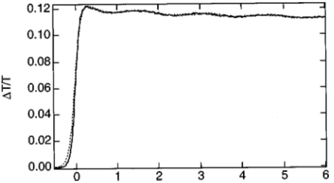
Figure 1 shows the measured probe transmission change as a function of probe delay for a 62 Å well-width MWQ for a pump wavelength of 394 nm. After the pump excited car-riers in the quantum wells and caused transmission increases
at zero time delay, a clear cosine-like transmission oscilla-tion was observed. The observed oscillaoscilla-tion frequency was found to be independent of pump/probe photoenergy and pump fluence. We attribute this large oscillation to coherent longitudinal–acoustic 共LA兲 phonon oscillation in the QW growth direction 共c axis兲. The observed oscillation period was 1.5 ps, corresponding to a frequency of 0.67 THz. The phase component of the cosine argument was always close to zero, with a time delay less than the pulse width, suggesting that the excitation of the oscillation was displacive4 and the system was under a new equilibrium position due to carrier screening after photoexcitation.18 The corresponding pump fluence and generated carrier density were 160J cm⫺2and 1.1⫻1012cm⫺2/per-well. When the pumped carriers screened the tensile-strain共in the c axis兲 -induced piezoelec-tric field and cause the opposite charged ions to oscillate away from or toward each other, the piezoelectric field will be increased or reduced with a modulated quantum-confined Stark effect. The electron–hole wave-function overlap will thus be modulated and reflected in probe transmission changes. This conforms to the observed cosine oscillation on top of the transmission change background observed in Fig. 1. For the trace of Fig. 1, the total transmission changes ⌬T/T is on the order of 10⫺1. Large transmission
modula-tion due to coherent acoustic-phonon oscillamodula-tion on the order of 10⫺2 was easily observed with a generated two-dimensional carrier density of 1⫻1012cm⫺2per well.
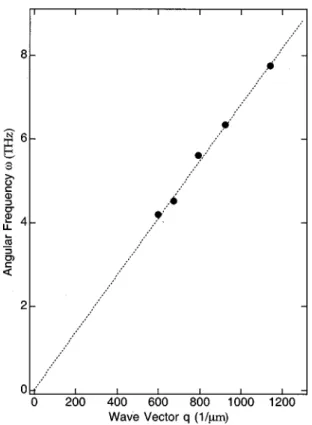
With different periodic distributions of the photoexcited carrier population, carriers are coupled to the selective acoustic-phonon mode with wave vector q corresponding to the inverse period width with q⫽2/a, where a is the MQW period width. Figure 2 shows the normalized probe transmission changes as a function of probe delay for differ-FIG. 1. Measured transient transmission changes vs probe delay for 62/43 Å
InGaN/GaN MQW. The dotted line is a convolution fit using a positive cosine oscillation with a period of 1.5 ps.
FIG. 2. Normalized transient transmission changes vs probe delay for dif-ferent MQWs. Traces are vertically displaced for clarity.
1250 Appl. Phys. Lett., Vol. 75, No. 9, 30 August 1999 Sunet al.
ent MQWs with photon energies above the quantum-well band gap. The oscillation frequency varies from 1.23 THz for a QW period of 55 Å共12 Å well兲 to 0.67 THz for a QW period of 105 Å 共62 Å well兲. Figure 3 plots the observed acoustic-phonon angular frequency versus the excited pho-non wave vector, which is a function of period width. A linear relation is observed. The slope of the linear relation corresponds to a sound velocity of 6800 m/s for the LA mode in the关0001兴 direction in wurzite GaN. Our measured value agrees well with the previously obtained LA mode c-axis sound velocity of 6620⫾220 m/s, which is derived from the results of an elastic stiffness constant c33
computa-tion at room temperature using the mean-square displace-ment of GaN measured by an x-ray method,19 assuming a density of 6.095 g/cm3. This supports our hypothesis that the observed oscillation is due to coherent acoustic-phonon os-cillation in the GaN MQW.
In summary, we have observed coherent acoustic-phonon oscillation in InGaN/GaN multiple-quantum wells.
This oscillation is induced by the coupling between the pe-riodic carrier population and the corresponding acoustic-phonon mode. After femtosecond pulse excitation, photoge-nerated carriers will screen out the strain-induced piezoelectric field and initiate this coherent acoustic-phonon oscillation. The resulting modulation of the piezoelectric field will then cause large optical property oscillation through the quantum-confined Stark effect. Transmission changes on the order of 10⫺2 can thus be easily observed. Our work opens the way to the studies of the properties of acoustic phonons and their interactions with surrounding car-riers in semiconductors.
The authors would like to acknowledge stimulating sci-entific discussions with Professor E. P. Ippen, Professor D. H. Reitze, and Professor Y.-M. Chang. This work is sup-ported by the National Science Council of R.O.C 共Taiwan兲 under Grant No. NSC 88-2112-M-002-003. C. J. S. acknowl-edges support from NSF through Grant No. DMR 9817828.
1G. C. Cho, W. Kutt, and H. Kurz, Phys. Rev. Lett. 65, 764共1990兲. 2W. Kutt, G. C. Cho, T. Pfeifer, and H. Kurz, Semicond. Sci. Technol. 7,
B77共1992兲.
3T. Pfeifer, W. Kutt, H. Kurz, and H. Scholz, Phys. Rev. Lett. 69, 3248
共1992兲.
4T. K. Cheng, J. Vidal, H. J. Zeiger, G. Dresselhaus, M. S. Dresselhaus,
and E. P. Ippen, Appl. Phys. Lett. 59, 1923共1991兲.
5
W. Albrecht, T. Kruse, and H. Kurz, Phys. Rev. Lett. 69, 1451共1992兲.
6A. V. Kuznetsov and C. J. Stanton, Phys. Rev. B 51, 7555共1995兲. 7E. R. Thoen, G. Steinmeyer, P. Langlois, E. P. Ippen, G. E. Tudury, C. H.
Brito Cruz, L. C. Barbosa, and C. L. Sedar, Appl. Phys. Lett. 73, 2149 共1998兲.
8A. Harata, H. Nishimura, and T. Sawada, Appl. Phys. Lett. 57, 132
共1990兲.
9M. D. Fayer, IEEE J. Quantum Electron. 22, 1437共1986兲. 10
P. Basse´ras, S. M. Gracewski, G. W. Wicks, and R. J. D. Miller, J. Appl. Phys. 75, 2761共1994兲.
11N.-H. Lin, H. J. Maris, L. B. Freund, K. Y. Lee, H. Luhn, and D. P. Kern,
J. Appl. Phys. 73, 37共1993兲.
12H. T. Grahn, D. A. Young, H. J. Maris, J. Tauc, J. M. Hong, and T. P.
Smith III, Appl. Phys. Lett. 53, 2023共1988兲.
13A. Yamamoto, T. Mishina, and Y. Masumoto, Phys. Rev. Lett. 73, 740
共1994兲.
14A. Bartels, T. Dekorsy, H. Kurz, and K. Ko¨hler, Phys. Rev. Lett. 82, 1044
共1999兲.
15
S. Nakamura and G. Fasol, The Blue Laser Diode 共Springer, Berlin, 1997兲.
16T. Takeuchi, S. Sota, M. Katsuragawa, M. Komori, H. Takeuchi, H.
Amano, and I. Akasaki, Jpn. J. Appl. Phys., Part 2 36, L382共1997兲.
17
C.-K. Sun, Y.-L. Huang, J.-C. Wang, S. Keller, M. Mack, U. K. Mishra, and S. P. DenBaars, in Technical Digest of the Conference on Laser and Electro-optics, Baltimore, MD, Paper No. CTuI4共1999兲.
18L. H. Peng, C. W. Chung, and L.-H. Lou, Appl. Phys. Lett. 74, 795
共1999兲.
19
V. A. Savastenko and A. U. Sheleg, Phys. Status Solidi A 48, K135 共1978兲.
FIG. 3. Measured angular frequency of oscillation vs carrier wave vector for different MQWs. The dashed line corresponds to a sound velocity of 6800 m/s.
1251 Appl. Phys. Lett., Vol. 75, No. 9, 30 August 1999 Sunet al.