Yu and Chen: Design of an Efficient VLSI Architecture for 2-D Discrete Wavelet Transforms 135
DESIGN OF AN EFFICIENT VLSI ARCHITECTURE FOR
2-D DISCRETE WAVELET TRANSFORMS
Chu Yu and Sao-Jie Chen Department of Electrical Engineering
National Taiwan University Taipei, Taiwan, R.O.C.
Abstract
In this paper, we present a VLSI architecture for the separable two-dimensional Discrete Wavelet Transform (DWT) decomposition. Using a computation-schedule table, we showed how the proposed separable architecture uses only a minimal number of filters to generate all levels of DWT computations in real time. For the computation of an N x N 2-D DWT with a filter length L , this architecture spends around N 2 clock cycles, and requires 2NL-2N storage unit, 3L multipliers, as well as 3(L-1) adders.
1. Introduction
The wavelet transform (WT) provides an alternative approach to signal processing, especially suited for the analysis of spatial and spectral locality. In recent years, there has been a number of studies on wavelet transforms for signal analysis and synthesis [ 11-[3]. Generally, the 2- D DWT is frequently applied in image [4]-[7] and video [8]-[9] processing. However, as other 2-D transforms, DWT still needs a large amount of computation; in order to meet the requirements of fast computation in real-time applications, dedicated hardware implementations are required.
Several VLSI architectures [lo]-[ 181 have been proposed for 2-D DWT’s. For instance, Lewis and Knowles [ l o ] firstly proposed a multiplierless 2-D architecture for the 4-tap Daubechies wavelet transform. Vishwanath et al. [ l l ] presented a 2-D systolic-parallel DWT architecture that uses a combination of systolic and parallel filters.
Chakrabarti et al. [ 121-[ 131 devised many efficient architectures, such as parallel filters (in 1-D and 2- D), SIMD linear array, and SIMD multigrid architectures, which utilize parallel structures to implement the existing pyramid [ 11 and “ a trous” [ 141 algorithms for the DWT and the continuous WT, respectively. A parallel pipelined VLSI array architecture for the 2-D DWT has also been proposed by Chuang and Chen [15]. Moreover, many other hardware implementations of the 2-D DWT have been presented in [16]-[ 181.
In this paper, we design a VLSI architecture for the separable 2-D DWT decomposition. The computations of the architecture are accomplished according to a computation-schedule table generated b y the data dependence analysis of the separable 2-D DWT. Form this table, we observe that the proposed architecture eliminates the intermediate hardware requirements between resolution levels and minimizes the filters used in the architecture. Since the architecture spends lower hardware cost and has a regular hardware structure, it is suited for single- chip VLSI implementation.
2.
2-D DWT Architecture
A . Preliminaries
The input signals in 1-D DWT are transformed into a high (H) and a low ( L ) component signals by a 1-D filter bank. Similar to the 1-D case, 2-D DWT separates an array of input signals into four signal bands, i.e., the high-high
(HH),
high-low ( H L ) , low-low ( L L ) , and low-high ( L H ) component signals by using a 2-D filter bank. Figure 1136 IEEE Transactions on Consumer Electronics, Vol. 45, No. 1, FEBRUARY 1999
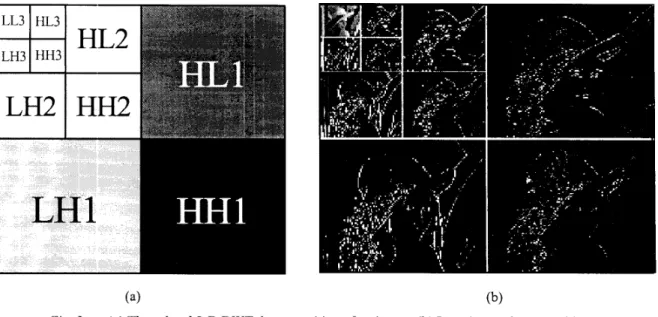
Fig. 2. (a) Three-level 2-D DWT decomposition of an image. (b) Lena image decomposition.
illustrates one level of separable 2-D WT decomposition, and Fig. 2 shows a three-level 2-D DWT decomposition of the Lena image.
...
... ...,
I ; HF j
_
... ~
...
@
: keep one column out of two0
I
b
: keep one row out of two Fig. 1. One-level of separable 2-D WT decompositionFor an N x N input image processed through m levels of 2-D DWT decompositions, the total number of filtering computations iterating on the lowpass (or highpass) filter only is given by:
According to the above equation, the upper bound on
the number of lowpass (or highpass) computations is
4 .
This implies that the separable approach needs two lowpass and two highpass filters for ali the computations of an m-level2-D DWT.Next, consider that an N x N image is fed into the separable architecture using the direct implementation as described in [ l l ] . An amount of 2 N 2 clock cycles is needed to compute the N row DWT's. Similarly, 2 N 2 cycles are required to compute the N column DWT's. Thus, the computation time of this separable architecture in total is 4 N 2 clock cycles. Also, since the first output value is generated after computing all the row DWT's, the architecture latency is N clock cycles. Moreover, it needs N2memory space to store all the filtering output coefficients.
B. Proposed Separable 2 - 0 D WT Architecture
The direct implementation [ 111 which makes use of 1-D DWT modules is a straightforward realization of the 2-D DWT. Clearly, its advantage is easy to realize, but the latency is too long and the needed memory space is large. Owing to these shortcomings, the direct approach is not widely used in practice. Moreover, the above shortcomings can be improved by the systolic-parallel architecture proposed in [ 111, which uses only two systolic and four parallel filters to generate all levels of the 2-D DWT
Yu and Chen: Design of an Efficient VLSI Architecture for 2-D Discrete Wavelet Transforms 137
Storage Unit
w
L, LLW LLL, ...IN
LL, LLLL,
. . .
LH, LLLH,
...
HL, LLHL,
...
HH, LLHH,
...
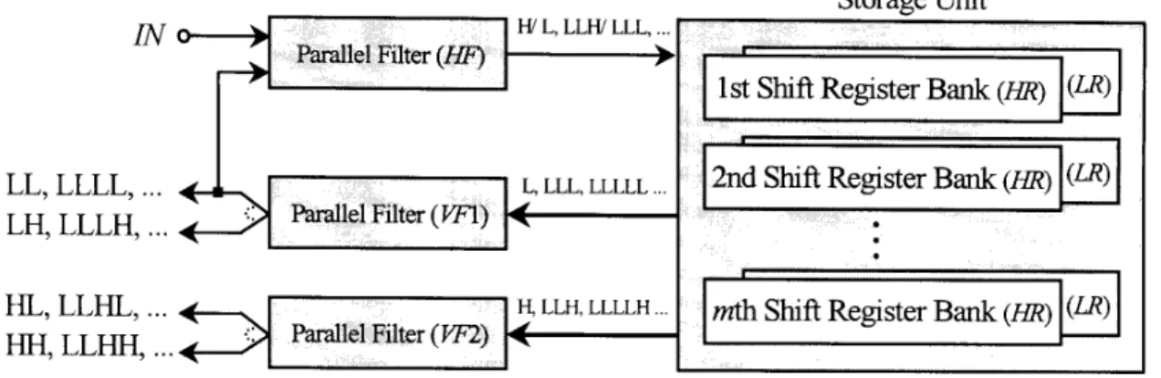
Fig. 3, Proposed VLSI architecture
the computation time and the hardware cost, we propose a VLSI architecture in Fig. 3 for the implementation of a separable 2-D DWT.
z
...
I"+
+
Highpass: hg! + h , t ' + . . . + h g "
Lowpass: gg! + g , r
'
+ . . . + gg"Fig. 4. Parallel filter structure
The proposed architecture consists mainly of three parallel filters and a storage unit. The parallel filter structure is similar to the one described in [ 131, as shown in Fig. 4. First, the horizontal filter HF is used to generate a highpass filtering output ( H ) at a positive clock cycle and a lowpass filtering output (L) at a negative clock cycle, respectively, as shown b y the dash-line block HF in Fig. 1. These two resultant filtering outputs will be stored in the corresponding lowpass (LR) and highpass (HR) register banks. Then, the two horizontal filtering outputs ( H and L) stored in the above register banks can b e further
VF2 respectively, to generate the four vertical filtering outputs. Similar to the case of horizontal filter HF, the highpass filtering outputs, HH from VF2 and L H from VF1, are generated at a positive clock cycle and the lowpass filtering outputs, HL from VF2 and L L f r o m VF1, are generated at a negative clock cycle. These two filters correspond to the dash-line blocks VF1 and VF2 in Fig. 1. Finally, all the resolution levels of D W T ' s can b e iteratively generated by the filters HF, VFI, and VF2, where a current level of filtering data is computed in the exact idle cycles of a previous level. The storage unit as shown in Fig. 3 is composed of m register banks. Each register bank, similar to the structure described in [17], is used to temporarily store the filtering data that have been output from HF and will serve as the input for the vertical filtering computations.
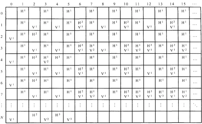
To explore how our proposed architecture works, we use a computation-schedule table to illustrate three levels of separable 2-D DWT computations for an N x N image as shown in Table 1, where H i and Vi are respectively the horizontal and vertical filtering computations at a resolution level i. For simplicity, only computations V i of single vertical filter (may be V F l or VF2) are shown in this table. This schedule table is generated by the data dependence analysis of a separable 2-D DWT. A horizontal filtering computation is shown in the upper side of a grid in the table and a vertical filtering computation is shown in the lower side. An upper- or a lower-sided blank grid represents no filtering computation there. All the resolution levels of computations are scheduled in this
138 IEEE Transactions on Consumer Electronics, Vol. 45, No. I , FEBRUARY 1999
Table 1 : Computation-Schedule Table for a Three-Level Separable 2-D DWT
0 1 2 3 4 5 6 7 8 9 1 0 I I 1 2 1 3 14 1 5 . . .
table. Form the table, assume that a raster scan is used, three levels of horizontal computation cycles occur at a grid (x, y ) that represents x column and y row as follows:
N
2 H I (2k+l, I )
H ' (4k+6, I )
H ' (8k+12,I)
for k 0 , I , 2, .,.,
-
- 1 and I=O, I , 2, ..., N - I ,for k O , I , 2, ..., - 1 and [=I, 3, 5, ..., N - I ,
f o r k = O , 1 , 2 ,,.., N - l a n d I = 3 , 7 , 1 1 , . . , N - I ,
8
Similarly, three levels of vertical computation cycles occur at: V (2k+2, I ) V' (4k+7,I) V ' : (8k+l3, I ) for k O , I , 2, ..., f o r k O , 1 , 2 ,..., N - l a n d I = 3 , 7 , 1 1 ,..., N - I , for k O , 1 , 2, ..., - 1 and I=1, 3, 5, ..., N - I , 2 4 8 - 1 and 1=7, 15, 23, ..., N - I .
Note that each of the last computation points of all levels will be wrapped to its next row except for H ' . For instance, the horizontal computation H 2 is wrapped to grids (2, I ) ,
for 1 = 2, 4,
. . .,
N;
and the vertical computation V ' appear at grids (0, I ) , for 1 = 2, 4, ...,N.
Therefore, all the resolution levels of computations shown in this schedule table are interleaved within spacing of the first-level. Computations without causing any computation collisions from the above equations.3. Performance Comparison of DWT
Arc hit ec ture s
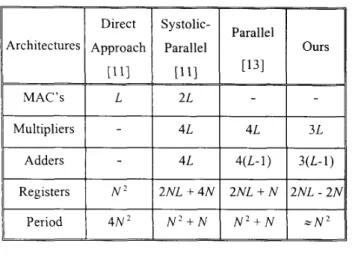
The performance comparison of our architecture and other similar architectures ([ 113 and [13]) is summarized in Table 2. For an N x N image, the proposed architecture needs around N
*
clock cycles to compute all the resolution levels of DWT's. Also, this architecture requires only three programmable parallel filters, a storage unit, and a control unit. Compared with other separable 2-D DWT approaches as shown in Table 2, our architecture is attractive in terms of both its hardware cost and computation time (period).Yu and Chen: Design of an Efficient VLSI Architecture for 2-D Discrete Wavelet Transforms 139
Architectures
TABLE 2: Comparisons of Various 2-D DWT Architectures
Direct Systolic-
Parallel
Approach Parallel Ours
MAC’S Multipliers 3L
- I
L 2L 4L 4L I I I III
Registers Period Adders1
-
I
4LI
4(L-1)I
3(L-1)
I/
N 2 2 N L + 4 N 2 N L + N 2 N L - 2 N 4 N 2 N ’ + N N ’ + N - N 24.
Conclusion
A fast and efficient 2-D DWT architecture has been described in this paper. The architecture utilized a computation-schedule table to accomplish all the resolution levels of computations. Since this architecture has a low latency, a low hardware cost, and ability to process 2-D digital signals in real-time, it can be applied very well to the codec implementation for various videohmage processing standards, such as MPEG-4 and JPEG-2000. For a video signal processing, the computation time of the architecture per picture spends about N 2 only, which meets the real-time requirement of many 2-D signal-processing applications.
5 . Acknowledgment
This paper was supported by the National Science Council, Taiwan, R.O.C., under grants NSC88-22 15-E002-037
6. References
[ 11 S. Mallat, “ A theory for multiresolution signal decomposition : The wave 1 et represent at i on, ”
IEEE Trans. Pattern Anal. and Machine Intell.,
vol. 11, no. 7, pp. 674-693, July 1989. [2] 0. Rioul and M . Vetterli, “Wavelets and
signal processing,” IEEE Signal Processing Magazine, vol. 8, no.4, pp. 14-38, Oct. 1991.
81
91
1. Daubechies, Ten Lectures on Wavelets. vol. 61 of CBMS-NSF Regional Conferences Series
in Applied M a t h e m a t i c s , S I A M, Philadelphia, PA, 1992.
S. Mallat, “Multifrequency channel decompositions of images and wavelet models,” IEEE Trans. A c o u s t . , Speech, Signal Processing, vol. 37 , no . 12, pp. 2091-2110, Dec. 1989.
M. Antonini, M. Barlaud. P. Mathieu, and 1. Daubechies, “Image coding using wavelet transform,” I E E E Trans. Image Processing. v’ol. 1 , no. 2, p p . 205-220, Apr. 1992.
J. M. Shapiro, “ E m b e d d e d image coding using zerotrees o f wavelet coefficients,” IEEE Trans. Signal Processing, vol. 4 1, no. 12, pp. 3445- 3462, Dec. 1993.
A . Averbuch, D . Lazar, and M. Israeli, “Image compression using wavelet transform and mu 1 tires o lu t i o n decomposition. ” IE E E Tra n J . Image Processing, vol. 5, no. 1, p p . 4-15, Jan.
1996.
A. S. Lewis and G . Knowles, “Video compression using 3 - D wavelet transforms.” Electron. Lett., vol. 26, no. 6, pp. 396-398, Mar. 1990.
K . H. Goh, J. J. Soraghan, and T. S. Durrani. “ N e w 3-D wavelet transform coding algorithm for image sequences,” Electron. Lett., vol. 29, no. 4 , p p . 401-402, Feb. 1993.
A. S . Lewis and G. Knowles, “VLSI architecture for 2-D daubechies wavelet transform without multipliers,” Electron. Lett., vol. 27, no. 2, pp. 171-173, Jan. 1991.
M. Vishwanath, R . Owens, and M . J . Irwin, “ V L S I architectures for the discrete wavelet transform,” IEEE Trans. Circuits and Systems I l , Analog a n d Digital Signal Processing, vol. 42, no. 5 , p p . 305-316, May 1995.
C. Chakrabarti and M . Vishwanath, “Efficient realizations of the discrete and continuous wavelet transforms: f r o m single chip implementations to mappings on SIMD array computers,” IEEE Trans. Signal Processing, vol. 43, no. 3 , p p . 759-771, Mar. 1995. [13] C. Chakrabarti, M . Vishwanath, R. Owens,
“Architectures for wavelet transforms: a survey,” J o u 8 w a l of VLSI Signal Processing, vol. 1 4 , no. 2, pp.171-192, Nov. 1996. M . Holschneider, R. Kronland-Martinet, J . Morlet. and Ph. Tchamitchian, “ A real-time algorithm for signal analysis with the help of the wavelet transform,” in Wavelets, Time- Frryuency Methods and Phase Space, J. M. Combes, A. Cirossmann, and Ph. Tchamitchian, Eds. Berlin: Springer, IPTI, 1989, pp. 286- 297.
H. Y . H . ( r h u a n g and L. Chen, “VLSI architecture Ibr fast 2D orthonormal wavelet transform,” Journal of VLSI Signal Processing, vol. 10, no. 3, pp.225-236, Aug. 1995.
R . Rumian, “ A n architecture for real-time wavelet image decomposition,” in Proc. IEEE I n t . Svmp. O I I Circuits and Systems, London,
England, May 1994, pp. 73-76.
C. Yu and S. J . Chen, “VLSI implementation of 2- D discrete wavelet transform for real time video signal processing,” IEEE Trans. on Consumer Electronic, vol. 43, no. 4, pp. 1270-1279, Nov. 1997.
J . D. Legat, J. P. David, and P. Desneux, “Programmable architectures for subband coding: FPGA-based system versus dedicated VLSI chip,” in Proc. the 2nd International Multiconference on
Computational Engineering in Systems Applications, CESA’98, Tunisia, April 1998, pp. 301-305.
IEEE Transactions on Consumer Electronics, Vol. 45, No. 1, FEBRUARY 1999
Chu Yu received the B.S. and M.S. degrees in electronic engineering from the National Taiwan Institute of Technology, Taipei, Taiwan, in 1991 and 1993, respectively. He is currently working towards the Ph.D. degree in the department of electrical engineering at National Taiwan University His research interests include VLSI architectures and speechhmage processing.
Sao-Jie Chen (S’85-M’88) received the B.S. and M.S. degrees in electrical engineering from the National Taiwan University, Taipei. Taiwan, ROC, in 1977 and 1982 respectively, and the Ph D. degree in electrical engineering from the Southern Methodist University, Dallas, USA, in 1988. Since 1982, he has been a member of the faculty in the Department of Electrical Engineering, National Taiwan University, where he is currently a professor. From 1985 to 1988, he was on leave from National Taiwan University and working toward his Ph.D at Southern Methodist University. During the fall of 1987, he held a visiting appointment at the Department of Electrical and Computer Engineering, University of Wisconsin, Madison. His current research interests include. VLSI physical design automation, fault-tolerant computing, object-oriented software engineering, and supercomputer architecture design and simulation. Dr. Chen is a member of the Chinese Institute of Engineers, the Association for Computing Machinery, the IEEE, and the IEEE Computer Society.