國 立 交 通 大 學
電子工程學系 電子研究所碩士班
碩士論文
鎳金屬矽化物誘導橫向結晶垂直通道
低溫複晶矽薄膜電晶體之研究
The Study of Vertical Channel Low
Temperature Polycrystalline Silicon Thin-Film
Transistors Fabricated by Ni – Silicide Induced
Lateral Crystallization Technology
研 究 生:賴久騰
指導教授:雷添福 博士
鎳金屬矽化物誘導橫向結晶垂直通道
低溫複晶矽薄膜電晶體之研究
The Study of Vertical Channel Low Temperatrue
Polycrystalline Silicon Thin-Film Transistors
Fabricated by Ni – Silicide Induced Lateral
Crystallization Technology
研 究 生:賴久騰 Student: Jiou-Teng Lai 指導教授:雷添福 博士 Advisor: Dr. Tan-Fu Lei
國 立 交 通 大 學
電子工程學系 電子研究所碩士班
碩士論文
A Thesis
Submitted to Department of Electronics Engineering & Institute of Electronics College of Electrical Engineering
National Chiao Tung University In Partial Fulfillment of the Requirements
For the Degree of Master of Science
in
Electronic Engineering June 2007
Hsinchu Taiwan Republic of China
鎳金屬矽化物誘導橫向結晶垂直通道
低溫複晶矽薄膜電晶體之研究
學生: 賴久騰
指導教授: 雷添福 博士
國立交通大學
電子工程學系 電子研究所碩士班
摘 要
在本論文中,首先研究以金屬誘導橫向結晶方法完成水平結構的複矽晶薄膜 電晶體。從文獻中發現傳統的金屬誘導結晶方式,是將鎳金屬直接鍍在所定義的 通道兩端後,再去做橫向誘導,使得通道兩端造成金屬污染,因此我們將鎳金屬 鍍在遠離通道處,以完成金屬誘導。由結果推論由於在沉積非晶矽閘極時,先前 非晶矽通道部分,已部分轉變成複晶矽薄膜通道,導致金屬誘導結晶時,電子遷 移率並沒有顯著的增加,但次臨界特性以及漏電有明顯的改善,因此,在第二個 部分,將改變結構,用後沉積非晶矽通道的底部閘極薄膜電晶體為主體,以保持 通道部分必為非晶矽薄膜,去做鎳金屬橫向誘導的研究。 有關垂直通道結構的複晶矽薄膜電晶體,以底部閘極結構的薄膜電晶體為構 想,垂直通道的長度部分主要是由閘極高度所控制並不受限於微影技術的限制,因此能以限有的微影機器,做出原本微影限制之下的線寬,而源極和汲極定義的 位置與原本頂部閘極結構的複晶矽薄膜電晶體一樣,是在閘極的兩端,因此在離 子佈值時,除了源極和汲極兩端之外,在閘極氧化物的頂部的複晶矽薄膜也是有 摻雜雜質的區域,此區域在傳統的底部閘極結構原本是通道區域,是由於本研究 的汲極源極定義位置,加上垂直通道是在閘極的左右兩側,因此造成此區域,在後 續的研究也會探討到這個區域是否對電性造成影響,而在此結構的電極安排使得 等效於一個雙閘極的電晶體結構,希望能增加閘極的控制能力,減少短通道效應 的發生。 接著,是延續垂直通道的研究,希望能有效的提升電子遷移率,因此以鎳金 屬誘導橫向結晶的方式使通道形成較大的結晶,減少矽晶粒之間的缺陷,而在初 步的研究,發現以鎳金屬直接誘導橫向結晶的方式,經由低溫長時間回火之後, 由於鎳金屬擴散的關係,完成誘導結晶之後,有過多的鎳金屬聚集在頂部參雜的 中間區域,而造成過多的缺陷累積,雖然電子遷移率有效的提升,但整體的電性 並不如預期,因此提出先形成鎳金屬矽化物後,將未反應的鎳金屬或金屬氧化物 去除之後,再進行鎳金屬矽化物誘導橫向結晶處理,經由結果觀察得知在頂部摻 雜區域部分沒有明顯的鎳金屬累積或污染,並且得到很好的整體電性,除了電子 遷移率有效提升之外,次臨界特性以及導通電流都能有效改善。
The Study of Vertical Channel Low Temperature
Polycrystalline Silicon Thin-Film Transistors
Fabricated by Ni – Silicide Induced Lateral
Crystallization Technology
Student: Jiou-Teng Lei
Advisor: Dr. Tan-Fu Lei
Department of Electronics Engineering &
Institute of Electronics
National Chiao Tung University
ABSTRACT
In this thesis, we first study about horizontal channel poly crystalline thin film transistors by metal induced lateral crystallization (MILC). It is known that nickel deposition on source and drain regions cause metal contaminations on these regions after the MILC process. Thus we use nickel deposition on offset regions of metal to complete the MILC process. Because the result of the experiment shows that the field effective mobility has no remote effect after the MILC process even though the sub-threshold swing and leakage are reduced effectively, we infer that the a-Si channel film has be transferred to poly-Si during the deposit of a-Si gate rather than
the MILC process. Thus in the next part of the thesis, the device structure is changed: the structure would be based on button gate thin film transistors, which would keep a-Si channel due to it is deposited after poly Si gate.
With the vertical channel poly crystalline thin film transistors, the idea based on button gate structure thin film transistors, the vertical channel length is defined by gate electrode height rather than lithography technology. We can then fabricate this device, which has shorter channel size by lithography machine (G-Line stepper), and the source/drain regions is the same as the traditional top gate thin film transistors defined at both sides of the gate. When the source/drain implants, the floating N+(P+) region is formed on the gate electrode because of the design positions of source, drain and channel regions. We will further discuss the influence of this floating region as well as how this vertical structure is equivalent the dual gate thin film transistor due to the arrangement of electrodes. We hope that it can induce the gate’s controllability and reduce the short channel effect
The study of vertical channel with high field effect mobility by Ni induced lateral crystallization, which can form larger grains on channel regions and reduce grain boundary defects. We detect the method of Ni induced lateral crystallization through high field effective mobility, but that accumulates too much Ni on floating N+ (P+) region and causes defects and metal contamination. As Ni is used to form silicde and then proceed to low temperature annealing, we can observe the floating region that has no Ni acumination regions or contaminations. This aids us in obtaining good electronic performance of this device, not only the remote field effective mobility but also the vast improvement of sub-threshold swing and on/off currents.
誌謝
兩年的碩士生涯終於完成了,首先感謝雷添福老師,在老師開明的管教方式 之下,使得我們能夠依照自己的興趣,去完成我們的研究,並且給予意見、糾正 我們的錯誤,除此之外,老師非常地和藹可親並且時時關心我們的生活狀況,由 於老師的關心和指導,使我們更能順利的完成研究 另外感謝電物所趙天生老 師,在每次參加趙老師實驗室的討論時,總是討論熱烈並且獲益良多,讓我學到 很多東西。 接著,特別感謝郭柏儀學長的細心指導,由於他的經驗豐富,以及做實驗的 認真態度,讓我在研究方面能更加順利,還有智揚學長、家文學長,謝謝你們常 在我遇到問題的時候,給予我適時的幫助、解答,而在每次的小組討論時,感謝 紹明學長和俊嘉學長的教導,讓我更加了解有關記憶體方面的研究,還有我同屆 的同學們,仕傑、明爵、哲綸、文呈、士銘、文瑋、廷圍,和你們一起無論是修 課、討論、打球甚至是有時令人苦悶的實驗時間,因為有了你們,都變得相當有 趣,而碩一的學弟妹們:子恆、張婷、冠良、文彥、春瑀,謝謝你們平時幫忙, 也祝你們研究順利,再來謝謝電物所的學長、同學和學弟們,讓我在做實驗時, 得到許多幫助,此外謝謝在求學生涯中,所有認識的的師長、學長、同學和學弟 妹們,謝謝你們的指導和幫忙。 最後感謝我的家人,謝謝我的父親賴演超先生及母親陳彩宜女士,謝謝他們 教導我做人處事、學習的態度,讓我培養出健全的待人處事的方式,另外也謝謝 我的姑姑,謝謝他給予我適時鼓勵、支持,使我更順利完成學業,還有我的大姐、 大哥、二姐,你們的努力和教導,都成為了我學習的榜樣,因此,我由衷地感謝 家人帶給我的一切,最後以此論文獻予你們。Contents
Abstract (Chinese)... I Abstract (English)... III Acknowledge...V Contents………...VI Table & Figure Captions………...………...VIII
Chapter 1 Introduction………...1
1.1 Overview of Poly-Si Thin-Film Transistors...1
1.2 Overview of Vertical Thin-Film Transistors...2
1.3 Overiew of Metal Indeuced Lateral Crystallization Thin Film Transistors...3
1.4 Motivation...4
1.5 Thesis Organization...5
Reference...6
Chapter 2 Characteristics of Conventional Low Temperature Nickel Induced Lateral Crystallization Poly-Si TFTs………...…10
2.1 Introduction ...10
2.2 Experimental...11
2.3 Method of Device Parameter Extraction………....13
2.3.2 Determination of Subthreshold Swing……….………13
2.3.3 Determination of Field Effect Mobility………14
2.3.4 Determination of ON/OFF Current Ratio……….14
2.4 Results and Discussion...15
2.5 Summary...16
Reference...29
Chapter 3 Characteristics of Vertical Channel Low Temperature Nickel Induced Lateral Crystallization Poly-Si TFT...30
3.1 Introduction...30
3.2 Experimental...31
3.3 Results and Discussion...32
3.4 Summary...34
Reference...57
TABLE CAPTIONS
Chapter 2
Table2.1 Comparison of device characteristics of the conventional-TFTs and NSILC-TFTs and MILC-TFTs
Chapter 3
Table3.1 Comparison of device characteristics of the conventional-TFTs and NSILC-TFTs and MILC-TFTs
Table3.2 Comparison of device characteristics of the NSILC-TFTs with same mask length and the different mask width.
Table3.3 Comparison of device characteristics of the NSILC-TFTs with same mask width and different mask length..
FIGURE CAPTIONS
Chapter 2
Fig.2.1 The schematic cross-section diagrams and key process flows of the devices. Fig.2.2(a) The top view of test key after MILC process and(b) The top view of device
after MILC process.
Fig.2.3 The top view of test key after NSILC process. Fig.2.4 The top view of different process.
Fig.2.5 Transfer characteristics of NSIILC-TFTs and Control-TFTs.
Chapter 3
Fig.3.1 The schematic cross-section diagrams and key process flows of the devices. Fig.3.2 Top view of different size patten after NSILC process.
Fig.3.3 Definition of effective channel width and length.
Fig.3.4 Transfer characteristics of NSILC-TFTs and Conventional TFTs.
Fig.3.5(a) Transfer characteristics of MILC-TFTs and NSILC TFTs and (b) Transfer conductance characteristics of MILC-VTFTs and NSILC-VTFTs.
Fig.3.6(a) Transfer characteristics of NSILC TFTs with different width and (b) Transfer characteristics of NSILC TFTs with different width.
Fig.3.7 Transfer characteristics of NSILC TFTs with different length.
Fig.3.8 Transfer characteristics of NSILC TFTs with different width and longer Length.
Fig.3.9 Transfer characteristics of NSILC TFTs with single and multi-channel. Fig.3.10 Transfer characteristics of NSILC TFTs with different multi-width size.
Chapter 1
Introduction
1.1 Overview of Poly-Si Thin-Film Transistors
In 1966, the first polycrystalline silicon thin film transistors (Poly-Si TFTs) were fabricated by C. H. Fa et al. [1]. So far, numerous research reports have been proposed to study the conduction mechanism, fabrication processes and device structures of the poly-Si TFTs in order to enhance the device performance. However, the research in poly-Si TFTs fabrication with temperature below 600°C was not commenced until 1980s. In the past twenty years, low-temperature polysilicon (LTPS) TFTs have been widely investigated in industrial applications, such as active-matrix liquid-crystal displays (AMLCDs) [2], high density static random access memories (SRAMs) [3], electrical erasable programming read only memories (EEPROM) [4][5] and candidate for 3-D ICs’ applications [6], etc. Within those applications, the application of active-matrix liquid-crystal displays (AMLCDs) is the major driving force to promote the developments of poly-Si TFT technology.
It is known that hydrogenated amorphous silicon (α-Si:H) TFTs were used for the pixel switching device at the first generation of AMLCDs. The advantages of α-Si:H TFTs are their compatibility with low processing temperature on large-area glass substrates and high off-stated impedance which result in a low leakage current. However, its low electron field effect mobility typically below 1 cm2V-1sec-1 has limited the development for AMLCDs technology. So, poly-Si TFTs have attracted much attention, because the field effect mobility in poly-Si is significantly higher than
that in α-Si, thus higher driving current can be achieved in poly-Si [7]. The higher driving current allows small-dimensioned TFTs to be used as the pixel switching elements, thus promoting the aperture ratio and the panel brightness, and therefore improving the performance of display.
The conduction mechanism and the performance of poly-Si TFTs are strongly related to grain boundaries and intragranular defects. For example, the defects in grain boundary would trap carriers and generate a potential barrier which degrades the on-stated current of poly-Si TFTs. Moreover, the grain boundaries also provide the path of leakage current. In order to obtain desirable electrical characteristics of poly-Si TFTs, several methods have been proposed to improve the device performance by enlarging the grain size of poly-Si films [8] and reducing the trap states in grain boundaries. It has been reported that the α-Si films can be crystallized by several techniques, such as SPC (solid-phase crystallization) [9], ELA (excimer laser annealing) [10][11] and MILC (metal-induced lateral crystallization) [12] to obtain a large grain size of poly-Si to raise the field effect mobility. Additionally, there were other methods such as plasma treatments to passivate the defects in the channel or narrowing the channel width to reduce the trap state density. We will make a discussion in next section.
1.2 Overview of Vertical Channel TFTs
Vertical thin film transistors (VTFT’s) are suitable for high density integration since their channel length are determined by the thicknesses of Si02 or polysilicon films instead of the photolithographic limitation. Much work had been devoted to developing andstudying VTFT’s [ 13]-[15].
self-aligned structure cannot be achieved. Another problem for TFT’s is that its leakage current, which is caused by the off-state drain field, is relatively large since it is a short channel device. The leakage current can be reduced by drain engineering such as by adding an offset structure [16]-[17]. However the offset structure needs an additional masking step which makes the fabrication for the device rather complicated and difficult.
VTFT structure which has the inherent off-set drain structure. The self-aligned feature eliminates the additional photolithographic step and the fabricated device exhibited submicron device characteristics.
1.3 Overview of Metal Induced Lateral Crystallization
Low-Temperature (500°C) formation of poly-Si thin film transistors (TFT's) on glass substrates is inevitable for large-area, high-definition liquid crystal display (LCD) application. The most widely used method for poly-Si preparation is the deposition of a-Si and its crystallization by post annealing such as solid phase crystallization (SPC) , excimer laser annealing (ELA) [18]. SPC has many advantages over ELA, such as simplicity, low cost, uniformity, and large area capability. But the high-crystallization temperature around 600" C prevents SPC from commercial application..Conventionally, poly-Si films are made by solid phase crystallization (SPC) of amorphous Si (a-Si) at 600°C. When some metals are added into a-Si, the crystallization temperature can be lowered below 600°C, and this phenomenon is known as metal-induced crystallization (MIC)[19]-[20] .For a successful application of MIC to devices, however, the significant incorporation of Ni in the MIC polycrystalline silicon (poly-Si) films [21] might limit the potential improvement in the performance of the thin film transistors (TFT’s) realized on such films.
Subsequently, metal induced lateral crystallization (MILC) has been proposed [22] as a better alternative to MIC, The formation process of the NiSi2 precipitate strongly depends on the sample condition such as Ni/Si ratio. When a Ni film is deposited on Si and annealed, the inter-reaction follows two steps: first step is Ni2Si to NiSi and second step is NiSi to NiSi2 .The silicide formation proceeds sequentially, which means that the metal/silicon diffusion leads to the successive formation of the silicides, starting form the metal-rich to end up to the silicon-rich silicide. Small NiSi2 precipitates aggregate together and become big precipitates and the needles come from the big precipitates resulting in poly-Si films with reduced Ni incorporation and large elongated grains—the long axes of which are parallel to the direction of the grain.
Recently, metal-induced lateral crystallization (MILC) phenomenon was reported for palladium, nickel, aluminum , where large gains over several tens of microns are obtained. The Si grains, however, contained many microtwin defects which are unfavorable for TFT application [23]. After the discovery of Ni- MILC where microtwin-free Si grains are obtained, Low temperature TFT’s with high field effect mobility have been fabricated [24]–[26], thus establishing MILC as a potentially enabling technology for realizing systems requiring low process temperature yet with high performance transistors—such as the active matrix liquid crystal displays with on-panelintegrated driver circuits.
1.4. motivation
We fabricate vertical-channel poly-Si TFTs by using Ni-silicide induced lateral crystallization (NSILC-VTFTs), due to Ni-silicide induced lateral crystallization(NSILC) can enlarge the channel grain size in specific orientation. The
devices can eliminate metal contaminations on source and drain region due to the metal seed window is arranged on source and drain contact sides [27] We hope that the grain is large enough to single large grain in vertical channel region after low temperature annealing and the drain-side and source-side grain boundaries touch in floating n+ (p+) region after NSILC process due to the mask layout arrangement [28]. The performances of the NSILC-VTFTs are not degraded by metal contaminations and grain boundaries induced from S/D sides due to the floating n+ (p+) region. Therefore, the NSILC-VTFTs are S/D symmetric devices and effective dual gate structures. We hope that measured results shows the NSILC-VTFTs have high field effect mobility, small S.S., low leakage current.
1.5 Organization of the thesis
In Chapter 2, we will proof that the nickel silicide induced lateral crystallization (NSILC) is less contaminations and Ni accumulations than traditional metal indued lateral crystallization (MILC), and then we fabricate the conventional structure device with the NSILC process, as result, we observed that the field effect mobility was not increased obviously due to the fabrication problem, we will discuss this problem and solve it in chapter 3.
In Chapter 3, we fabricated the vertical channel structure TFTs with NSILC process(NSILC-VTFTs ) to solve the problem of chapter 2, and we will discuss the influences of the vertical structure and compare with MILC-TFTs and NSILC-VTFTs .At the end of this thesis, we make some conclusions and future work in Chapter 4.
Reference
[1] C. H. Fa, and T. T. Jew, “The polysilicon insulated-gate field-effect transistor,” IEEE Trans. Electron Devices, vol. 13, no. 2, pp. 290, 1966.
[2] Y. Oana, “Current and future technology of low-temperature poly-Si TFT-LCDs,” Journal of the SID, vol. 9, pp. 169-172, 2001.
[3] S. Morozumi, K. Oguchi, S. Yazawa, Y. Kodaira, H. Ohshima, and T. Mano, “B/W and color LC video display addressed by poly-Si TFTs,” SID Dig., pp.156, 1983. [4] R. E. Proano, R. S. Misage, D. Jones, and D. G. Ast, “Guest-host active matrix
liquid-crystal display using high-voltage polysilicon thin film transistors,” IEEE Trans. Electron Devices, vol. 38, pp. 1781, 1991.
[5] S. Batra, “Development of drain-offset (DO) TFT technology for high density SRAM’s,” Extended Abstracts, vol.94-2, in Electrochemical Soc. Fall Mtg., Miami Beach, FL, Oct. pp. 677,1994.
[6] M. Cao, et al., “A simple EEPROM cell using twin polysilicon thin-film transistors,” IEEE Trans. Electron Devices, vol. 15, pp. 304, 1994.
[7] N. D. Young, G. Harkin, R. M. Bunn, D. J. McCulloch, and I. D. French, “The fabrication and characterization of EEPROM arrays on glass using a low temperature poly-Si TFT process,” IEEE Trans. Electron Devices, vol. 43, pp. 1930-1936, 1996.
[8] K. Banerjee, S. J. Souri, P. Kapur, and K. C. Saraswat, “3-D ICs: a novel chip design for improving deep-submicrometer interconnect performance and system-on-chip integration,” Proceedings of the IEEE, vol.89, pp. 602-633, 2001. [9] W.G. Hawkins, “Polycrystalline-silicon device technology for large-area
electronics”, IEEE Trans. Electron Devices, vol. 33, pp. 477-481, 1986.
[10] H. Kuriyama et al., “Enlargement of poly-Si film grain size by excimer laser annealing and its application to high-performance poly-Si thin film transistor,”
Jpn. J. Appl. Phys., vol. 30, pp. 3700-3703, 1991.
[11] A. Nakamura, F. Emoto, E. Fujii, and A.Tamamoto, “A high-reliability, low-operation-voltage monolithic active-matrix LCD by using advanced solid-phase growth technique”, IEDM Tech. pp.847, 1990.
[12] G. K. Guist, and T. W. Sigmon, “High-performance laser-processed polysilicon thin-film transistors,” IEEE Electron Device Lett., vol. 20, no. 2, pp. 77-79, Feb. 1999.
[13] T. Zhao, M. Cao, K. C. Saraswat, and J. D. Plummer, “A vertical submicron polysilicon thin-film transistor using a low temperature process,” IEEE Electron Device Lett., vol. 15, p. 415, 1994.
[14] S. D. S. Malhi, P. K. Chatterjee, T. D. Bonifield, J. E. Leiss, D. E. Carter, R. F. Pinizzotto, and D. J. Coleman, “Edge-defined self-alignment of submicrometer overlaid devices,” IEEE Electron Device Lett., vol. 5, p. 428, 1984.
[15] C. T. Liu, C. H. Douglas Yu, A. K. Kornblit, and K. H. Lee, “Inverted
thin-film transistor with a simple self-aligned lightly doped drain structure,” IEEE Truns. Electron Devices, vol. ED-39, no. 12, p. 2803, 1992.
[16] K. Tanaka, H. Arai, and S. Kohda, “Characteristics of offset-structure polycrystalline-silicon thin-film transistors,” IEEE Electron Device Lett., vol. 9, p. 23, 1988.
[17] Seki, O. Kogure, and B. Tsujiyama, “Laser-recrystalized polycrystalline- Silicon thin-film transistors with low leakage current and high switching ratio,” IEEE Electron Device Lett., vol. 8, p. 434, 1987.
[18] AT. Voutsas ”A new era of crystallization: advances in polysilicon crystallization and crystal engineering”,in Applied Surface Science 208-209(2003)250-262 [19] Gururaj A. Bhat, Zhonghe Jin, Hoi S. Kwok, and Man Wong “Effects of
ELECTRON DEVICE LETTERS, VOL. 20, NO. 2, FEBRUARY 1999
[20] Man Wong, Member, IEEE, Zhonghe Jin, Gururaj A. Bhat, Member, IEEE, Philip C. Wong, and Hoi Sing Kwok, Senior Member, IEEE “Characterization of the MIC/MILC Interface and Its Effects on the Performance of MILC Thin-Film Transistors” IEEE TRANSACTIONS ON ELECTRON DEVICES, VOL. 47, NO. 5, MAY 2000
[21] Z. H. Jin et al., “Ni induced crystallization of amorphous Si thin films on SiO ,” J. Appl. Phys., vol. 84, pp. 194–200, July 1998.
[22] S. W. Lee, Y. C. Jeon, and S. K. Joo, “Pd induced lateral crystallization of amorphous Si thin films,” Appl. Phys. Lett., vol. 66, pp. 1671–1673, March 1995.
[23] S. W. Lee and S. K. Joo, “Low temperature poly-Si thin film transistor fabrication by metal-induced lateral crystallization,” IEEE Electron Device Lett., vol. 17, pp. 160–162, April 1996.
[24] G. A. Bhat, Z. Jin, H. S. Kwok, and M. Wong, “Effects of longitudinal grain boundaries on the performance of MILC- TFT’s,” IEEE Electron Device Lett., vol. 20, pp. 97–99, Feb. 1999.
[25] Z. Jin, H. S. Kwok, and M. Wong, “Performance of thin film transistors with ultrathin MILC polycrystalline silicon channel layers,” IEEE Electron Device Lett., vol. 20, pp. 167–169, 1999.
[26] Darren Murley, Nigel Young, Michael Trainor, and David McCulloch
“An Investigation of Laser Annealed and Metal-Induced Crystallized Polycrystalline Silicon Thin-Film Transistors” IEEE TRANSACTIONS ON ELECTRON DEVICES, VOL. 48, NO. 6, JUNE 2001
Longitudinal Grain Boundaries on the Performance of MILC-TFT’s”IEEE
ELECTRON DEVICE LETTERS, VOL. 20, NO. 2, FEBRUARY 1999
[28] Horng-Chih Lin, Senior Member, IEEE, and Chun-Jung Su, Student Member,
IEEE “High-Performance Poly-Si Nanowire NMOS Transistors” IEEE
Chapter 2
Characteristics of Conventional Low
Temperature Nickel Induced Lateral
Crystallization Poly-Si TFTs
2.1 Introduction
Thin film transistors with high mobility and low leakage current are desirable in many applications especially in liquid crystal display (LCD) However, performance of TFTs is limited by the large amount of randomly oriented grain boundaries exist in the channel, which cause high threshold voltage, low On-current, gentle sub-threshold slope and high leakage current . Furthermore, the randomly nature of grain orientation leads to significant device-to-device variation, hence poor circuit yield.
To improve the performance of TFT, the crystallization methods such as laser crystallization [1], solid phase crystallization (SPC) [2], and metal induced lateral crystallization (MILC) [3] has been used to enlarge the grain size at the channel and reduce the number of grain boundaries. Recently, amorphous silicon (a-Si) was found to be crystallized by the catalytic effect of some metals [2] and this phenomenon is known as a metal-induced crystallization (MIC) [3]. For a successful application of MIC to device, however, problems related with metal contamination into the crystallized Si films must be solved [4].After the MILC process, the orientation of the
grain boundaries is no longer random, but aligns with the propagation direction of the recrystallization agent. As a result, the device performance can be better predicted if the effects of grain boundaries with a specific orientation are understood. , the effects of longitudinal (parallel to the direction of current flow) and latitudinal (perpendicular to the direction of current flow) grain boundaries on TFT are studied [5].
Therefore, we will fabricate the test structures with MILC process and nickel silicide induced lateral crystallization (NSILC) process in this chapter. And we will discuss the influence of the MILC and NSILC process in some photographs from optical microscope(OM), and we deicide to fabricate the conventional structure with NSILC process. As a result, we improve some electrical characteristics, but the fields effective mobility is not increased after induced crystallization process, so we will discuss this problem and suggest that how solve this problem.
2.2 Experimental
Bare Silicon covered with 5500 Å-thick SiO2 was used as the substrate. 500Å-thick a-Si thin film was deposited for active layer by Low pressure chemical vapor deposition (LPCVD) at 5500C, After patterning the a-Si layer to form active islands, a 500 Å-thick SiO2 thin film was deposited for gate dielectric by high density plasma chemical deposition (HDP-CVD). The 2000Å-thick a-Si was deposited by LPCVD to form gate electrode and then the 15kev, 5x1015 cm-2 As+ ion implantations were performed. Then 4000Å passivation was deposited by HDP-CVD, and the Ni-offset mask pattern was formed on the contact hole region. A 100Å-thick Ni and TiN thin films were deposited in the contact hole of the TFT’s and formed to NiSi by metal RTA. After RTA process, we remove residue Ni and TiN and then proceed to low temperature induced process ,which is the crystallization process and the dopant
activation process , the passivation 4000 Å is formed by PECVD and then contact hole and metal pad are defined at last , the fabrication process is completed. The schematic cross-section diagrams and key process flows of the devices are shown in Figure 2-1. Electrical properties were measured by HP4156.
2.3 Method of Device Parameter Extraction
In this thesis, all of the electrical characteristics of proposed poly-Si TFTs were measured by HP 4156B-Precision Semiconductor Parameter Analyzer. Many methods have been proposed to extract the characteristic parameters of poly-Si TFTs. In this section, those methods are described.
2.3.1 Determination of Threshold Voltage
Threshold voltage (Vth) is an important parameter required for the channel length-width and series resistance measurements. However, Vth is not uniquely defined. Various definitions have been proposed and the reason can be found in ID-VGS curves. One of the most common techniques is the linear extrapolation method with the drain current measured as a function of gate voltage at a low drain voltage of 50~100mV to ensure operation in the linear region [6]. The drain current is not zero when VGS below threshold voltage and approaches zero asymptotically. Hence the IDS versus VGS curve can be extrapolated to ID=0, and the Vth is determined from the extrapolated intercept of gate voltage (VGSi) by
2 DS GSi th V V V = − --- (Eq. 1.1)
Equation (1.1) is strictly only valid for negligible series resistance. Fortunately series resistance is usually negligible at the low drain current when threshold voltage measurements are made. The IDS-VGS curve deviates from a straight line at gate voltage below Vth due to subthreshold current and above Vth due to series resistance
and mobility degradation effects. It is common practice to find the point of maximum slope of the IDS-VGS curve and fit a straight line to extrapolate to ID=0 by means of finding the point of maximum of transconductance (Gm).
In this thesis, we use a simpler method to determinate the Vth called constant drain current method. The voltage at a specified threshold drain current is taken as the Vth. This method is adopted in the most studied papers of poly-Si TFTs. It can be given a threshold voltage close to that obtained by the complex linear extrapolation method. Typically, the threshold current is specified at (W/L)×10nA for VDS=0.1V and (W/L)×100nA for VDS=5V, where W and L are channel width and channel length, respectively.
2.3.2 Determination of Subthreshold Swing
Subthreshold swing (S.S.) is a typical parameter to describe the control ability of gate toward channel, which reflects the turn on/off speed of a device. It is defined as the amount of gate voltage required to increase/decrease drain current by one order of magnitude.
The S.S. should be independent of drain voltage and gate voltage. However, in reality, the S.S. increases with drain voltage due to channel shortening effect such as charge sharing, avalanche multiplication and punchthrough effect. The subthreshold swing is also related to gate voltage due to undesirable and inevitable factors such as the serial resistance and interface states.
In this thesis, the S.S. is defined as one-third of the gate voltage required to decrease the threshold current by three orders of magnitude. The threshold current is specified to be the drain current when the gate voltage is equal to threshold voltage.
2.3.3 Determination of Field Effect Mobility
Usually, field effect mobility (µeff) is determined from the maximum value of
transconductance (Gm) at low drain bias. The transfer characteristics of poly-Si TFTs are similar to those of conventional MOSFETs, so that the first order of I-V relation in the bulk Si MOSFETs can be applied to poly-Si TFTs. The drain current in linear region (VDS<VGS-Vth) can be approximated as the following equation:
(
)
⎥⎦⎤ ⎢⎣ ⎡ − − ⎟ ⎠ ⎞ ⎜ ⎝ ⎛ = 2 2 1 DS DS th GS ox eff DS V V V V L W C I µ --- (Eq. 1.2)where W and L are channel width and channel length, respectively. Cox is the gate oxide capacitance per unit area and Vth is the threshold voltage. Thus, the transconductance is given by DS ox eff GS DS m V L W C V I g ⎟ ⎠ ⎞ ⎜ ⎝ ⎛ = ∂ ∂ = µ --- (Eq. 1.3) Therefore, the field-effect mobility is
(max) →0 = DS V m DS ox eff g WV C L µ --- (Eq.1.4)
2.3.4 Determination of ON/OFF Current Ratio
On/off current ratio is one of the most important parameters of poly-Si TFTs since a high-performance device exhibits not only a large on-current but also a small off-current (leakage current). The leakage current mechanism in poly-Si TFTs is not like that in MOSFET. In MOSFET, the channel is composed of single crystalline Si and the leakage current is due to the tunneling of minority carrier from drain region to accumulation layer located in channel region. However, in poly-Si TFTs, the channel is composed of poly-Si. A large amount of trap state densities in grain structure attribute a lot of defect states in energy band gap to enhance the tunneling effect. Therefore, the leakage current is much larger in poly-Si TFTs than in MOSFET. When
the voltage drops between gate voltage and drain voltage increases, the band gap width decreases and the tunneling effect becomes much more severe. Normally we can find this effect in typical poly-Si TFTs’ IDS-VGS characteristics where the magnitude of leakage current will reach a minimum and then increase as the gate voltage decreases/increases for n/p-channel TFTs.
There are a lot of ways to specify the on and off-current. In this chapter, take n-channel poly-Si TFTs for examples, the on-current is defined as the drain current when gate voltage at the maximum value and drain voltage is 5V. The off-current is specified as the minimum current when drain voltage equals to 5V.
V V at Plot V I of Current Minimum V V at Plot V I of Current Maximum I I DS GS DS DS GS DS OFF ON 5 5 = − = − = --- (Eq. 1.5)
2.4 Result and Discussion
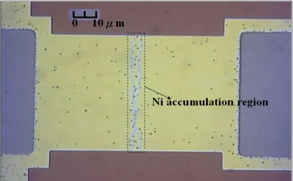
Fig.2-2(a),(b) show the top view of test key and device after MILC process, we can see many Ni precipitates in the mid-regions after MILC process, because of there are too many source of Ni transferred to NiSi which is acted seed or nucleus to excess saturation solubility, result of many Ni precipitates diffused during MILC process then caused contaminations or defects . We use two steps to complete this process, first step, we let Ni transfer to Ni-silicide by RTA process, second, we remove Ni or NiSiO2 before MILC process. When inducing process, less amount of Ni or Ni –silicide diffuses to induce crystallization, we observe Fig.2-3, which proofs this method can induce crystallization, we called this method Ni-silicide induced lateral crystallization (NSLIC), after NSILC process. In Fig2-4, compared with MILC and NSILC process, we can see there are not Ni precipitates or defects accumulation regions after NSILC process.
We can see the sub-threshold is improved obviously and the leakage is better than conventional-TFTs from Fig.2-5, but we observed the field effect mobility is not remote apparently , we suggested that the a-Si channel film was transferred to poly-Si film when we deposited a-Si gate by LPCVD, because of the situation and color of the channel film are the same after MILC process, so we make a test experiment , we deposited a-Si film on bare-Si wafer and then annealing 550 , thus,℃ we observed that the a-Si film is transferred to poly-Si ,so we detected that the pressure is too high (about 455mTorr) to let the a-Si transferred to poly-Si in the period of the furnace temperature ramps to set temperature, so we suggested that the purpose of MILC process was not apparent due to the evidence of the test experiment, but we obtained that the sub-threshold swing was improved obviously due to the defects are reduced when long activation time .
2.5 Summary
We compared with the metal induced lateral crystallization and nickel silicide induced lateral crystallization process, we observed that the nickel accumulation region after MILC process due to the nickel source or seeds are too more to excess the saturation solubility, and are caused metal contaminations in this region ,and then we use NSILC process to achieve this process, As the result, there are less Ni contaminations in induce regions, and then we fabricated the conventional TFTs with NSILC process, we observed that the subthreshold swing is improved obviously, but the field effective mobility is not remote effectively, we suggested that the a-Si film is transferred to poly-Si due to the pressure and the temperature is too high in furnace ramp period. So this situation is improved by some methods, which are low high –k and metal gate temperature process or bottom gate process.
(a) Deposit a-Si 500Å by LPCVD
(b)Define active region
(c)Deposit a-Si gate 2000Å by LPCVD
(e)Deposit passivation layer 4000 Å by PECVD
(g) Deposit Ni 100 Å and TiN 100 Å.
(i) Remove residue TiN and Ni and passivation.
(k) Define contact hole and deposit Al and the total process is completed.
MILC Process 500 oC, 12hr
NSILC Process, 500 oC, 12hr Fig. 2.4. The top view of different process
Fig.2.5 Transfer characteristics of NSIILC-TFTs and Control-TFTs.
V
DS= 0.1V, W/ L=10µm / 10µm
Without NH
3plasma Treatment
Gate Voltage V
GS( V )
-2
0
2
4
6
8
10
12
14
16
18
20
Drain Current I
DS( A )
10
-1310
-1210
-1110
-1010
-910
-810
-710
-610
-5Conventional TFTs
NSILC-TFTs
NSILC-TFTs
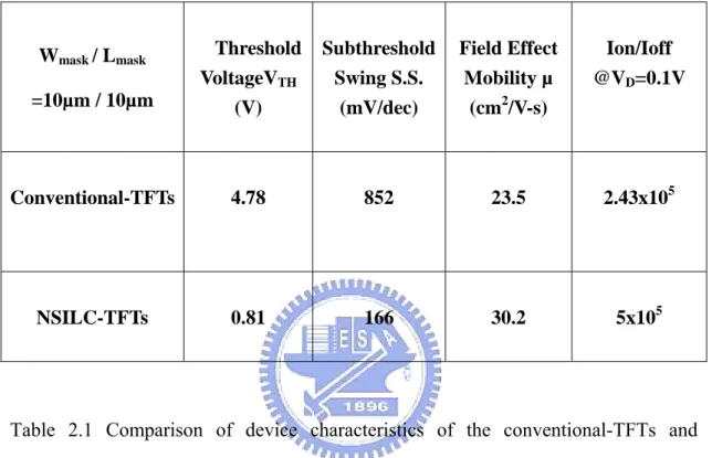
Wmask / Lmask =10µm / 10µm Threshold VoltageVTH (V) Subthreshold Swing S.S. (mV/dec) Field Effect Mobility µ (cm2/V-s) Ion/Ioff @VD=0.1V Conventional-TFTs 4.78 852 23.5 2.43x10⁵ NSILC-TFTs 0.81 166 30.2 5x10⁵
Table 2.1 Comparison of device characteristics of the conventional-TFTs and NSILC-TFTs
Reference
[1] AT. Voutsas ”A new era of crystallization: advances in polysilicon crystallization and crystal engineering”in Applied Surface Science 208-209(2003)250-262
[2] Seok-Woon Lee, Tae-Hyung Ihn, and Seung-Ki Joo “Fabricationof High-
Mobility p-Channel Poly-Si Thin Film Transistors by Self-Aligned Metal-Induced Lateral Crystallization”, IEEE ELECTRON DEVICE LETTERS, VOL. 17, NO. 8, AUGUST 1996
[3] Man Wong, Member, IEEE, Zhonghe Jin, Gururaj A. Bhat, Member, IEEE, Philip C. Wong, andHoi Sing Kwok, Senior Member, IEEE “Characterization of the MIC/MILC Interface and Its Effects on the Performance of MILC Thin-Film Transistors” ,IEEE TRANSACTIONS ON ELECTRON DEVICES, VOL. 47, NO. 5,
MAY 2000.
[4] Tae-Hyung Ihn *, Tae-Kyung Kim, Byung-Il Lee, Seung Ki Joo “A study on the leakage current of poly-Si TFTs fabricated by metal induced lateral
crystallization” in Microelectronics Reliability 39 (1999) 53-58.
[5] Gururaj A. Bhat, Zhonghe Jin, Hoi S. Kwok, and Man Wong “Effects of Longitudinal Grain Boundaries on the Performance of MILC-TFT’s” IEEE ELECTRON DEVICE LETTERS, VOL. 20, NO. 2, FEBRUARY 1999. [6] Darren Murley, Nigel Young, Michael Trainor, and David McCulloch“An
Investigation of Laser Annealed and Metal-Induced Crystallized Polycrystalline Silicon Thin-Film Transistors” IEEE TRANSACTIONS ON ELECTRON
Chapter 3
Characteristics of Vertical Channel Low
Temperature Nickel Induced Lateral
Crystallization Poly-Si TFTs
3.1 Introduction
In this topic, we study about vertical channel poly crystalline thin film transistors, this ideal which is based on button gate structure thin film transistors, the vertical channel length is defined by gate electrode height rather than lithography technology, so we can fabricate this device which has shorter channel size by lithography machine (G-Line stepper), and the source/drain regions is same of the traditional top gate thin film transistors which is defined both side of gate. When source/drain implant, the floating N+(P+) region is formed on gate electrode because of the design positions of source ,drain and channel region, we will discuss the influence of this floating region , and this vertical structure is equivalent the dual gate thin film transistor due to the arrangement of electrodes, we hope it can induce the gate Controllability and reduce short channel effect.
The study of vertical channel with high field effect mobility by Ni induced lateral crystallization, which can formed larger grains on channel regions and reduce grain boundary defects, we detect the method of Ni induced lateral crystallization through has high field effective mobility, but that has much Ni accumulation on
floating N+ (P+) region and caused defects and metal contamination, so we use Ni formed to silicde then proceed to low temperature annealing , we observe the floating region which has no Ni acumination regions or contaminations, and obtain good electronic performance of this device, not only remote field effective mobility but also sub-threshold swing and on/off currents can improve effectively.
3.2 Experimental
Bare Silicon covered with 5500 Å-thick SiO2 was used as the glass substrate. 2500 Å or 5000 Å-thick Poly-Si thin film was deposited for gate by low pressure chemical vapor deposition (LPCVD). After gate patterning, a 500Å-thick TEOS (tetra-ethyl-oxy-silane) gate oxide thin film was deposited by LPCVD. The 500Å-thick a-Si was deposited by LPCVD to form S/D and channel active region. Then a 4000Å passivation oxide was deposited by HDPCVD (high density plasma chemical vapor deposition), Ni-offset mask pattern was formed in the contact hole regions. A 100Å-thick Ni thin film was deposited on the contact hole of the TFTs. Using two methods to complete channel poly-Si crystallization process: one is conventional MILC process; another is our new NSILC process. The Ni-silicide of NSILC was achieved by RTA (rapid thermal annealing) at 450oC for 30 sec. Next, the residue Ni is removed by H2SO4 : H2O2 solution. Both methods were cystallized at 500oC for 12 hours. After removing the passivation oxide, the 15kev, 5x1015 cm-2 As+ ion implantations were performed. The activation of dopants was carried out by RTA annealing at 550oC. After contact and metal processes, all the devices were fabricated without NH3 plasma treatment for studying influences of grain boundaries. Electrical properties were measured on temperature-controlled stage with HP4156. The schematic cross-section diagrams and key process flows of the devices are shown in
Figure 3-1.
3.3 Result and discussion
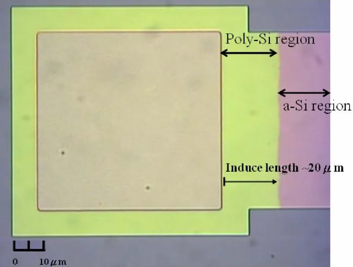
We observed that different size patterns have induced crystallization completely after 12 hours and there are not Ni precipitates or defect accumulation regions from Fig.3-2. Before measuring, We must define the device length and width from Fig.3-3, the top view of the mask length (Lmask) is equivalent to the floating region length of the device cross-section, and the effective channel length (Leff) is the vertical channel region, the top view of the mask width (Wmask) is equivalent our effective width, so we don’t defined another symbol.
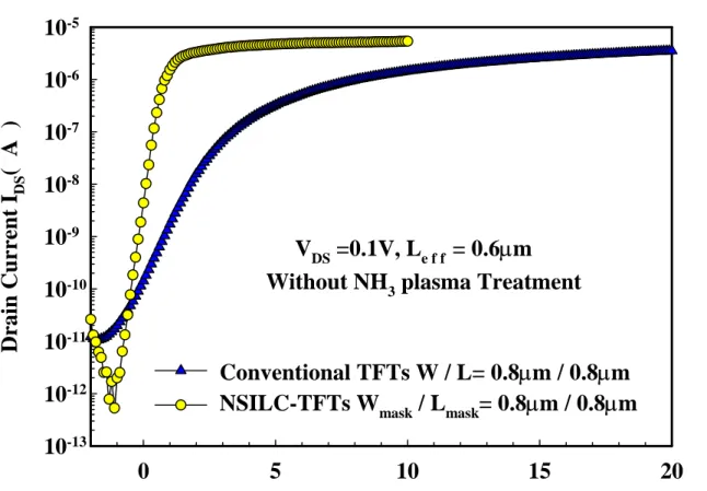
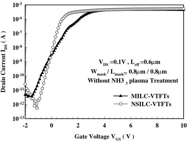
Fig. 3-4 shows transfer characteristics of NSILC-TFTs and conventional TFTs. We can see the NSILC-TFTs had good swing and low leakage and the threshold voltage is lower than conventional TFTs, so we suggested that the electrical characteristics of the NSILC were improved obviously due to the garin was larger after NSILC process than the conventional-TFTs ,which were crystallized by SPC process and then both NILC or NSILC-TFTs have higher mobility and on/off ratio from table 3.1 In Fig.3-5(a) shows the transfer characteristics of MILC-TFTs and NSILC-TFTs, the sub-threshold swing and leakage of NSILC-TFTs were reduced effectively due to the metal contaminations and defects of the NSILC-TFTs were eliminated, so we observed that the conductance of MILC-TFTs and NSILC TFTs from Fig. 3-5(b), we can know the field effect mobility of the NSILC-TFTs are larger than NILC-TFTs, Fig.3-6(a) shows the different width and short mask length, we can see the leakage and the sub-threshold swing are induced when the width increases[1]-[4], because of the large width has more Ni or NiSi2 seeds, which were induced crystallization and caused more grain boundaries or trap states in large width
regions[5]-[6].
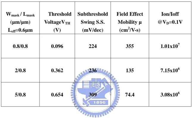
When the gate voltage increased ,the devices are transferred to the linear region, the on current increased slowly from Fig.3-6(b), as a result, the transconductance of different width don’t increase obviously due to more trap states or grain boundaries in larger width and the sub-threshold swing is increase, low conductance influenced the field effective mobility decrease obviously on table 3.2, we suggested that the mobility of larger width is degraded apparently due to more trap states and grain boundaries[7].
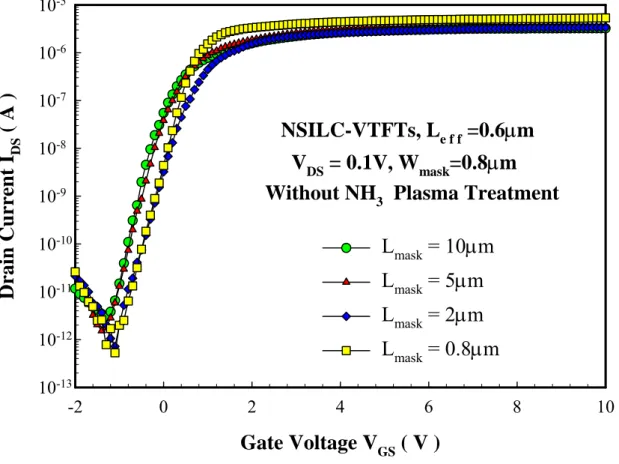
Fig.3-7 shows the same width and different mask length(floating region length), but the effective channel length are the same, so we will discuss the influence of the floating region length, we can see the shortest floating length has higher mobility ,good swing and high on/off ratio due to the crystallization regions of the shorter mask length with small width size are similar the single crystal[8], but when the floating region length increased, the induce distance must be longer ,so we suggested that the longer size region induced to crystallization is incomplete ,because of the induced speed is retard when the width size reduced, on the table3.3, we can observe that the performance of the device with minimum width and mask length is the best and the other devices with minimum width and larger mask length have similar field effect mobility[9]-[10], and we discussed that the devices with larger mask width; length and different width from Fig.3-13,we suggested that the shorter width has batter sub-threshold swing and leakage because less metal contaminations and grain boundaries than larger width size [11],we compared with Fig.3-11(a) and Fig 3-8, when the floating region length is larger, the sub-threshold swing and on-current is reduced due to more traps states in larger floating region[12].
Fig.3-9 shows the characteristics of NSILC-TFTs which have single channel or multi-channel , but the total width are similar, we can see the multi-channel device
has better subthreshold swing and lower leakage than single channel device[13]-[14], because of fewer NiSiseeds accumulated in smaller size width and then the occur probability of grain boundary is less than large width size. We can observe when the channel numbers increase doubly, the on and off currents are increase doubly. But the status of the single channel devices aren’t similar to multi-channel form Fig.3-10, we suggested that the single large width with more grain boundaries caused more traps stares or defects and then the on-current can’t increase doubly and the off-current increased.
3.4 Summary
We fabricated the NSILC and NILC-VTFTs successfully, and the electrical characteristics of NSILC or NILC-TFTs are better than conventional-TFTs, and the mobility and the sub-threshold are remote obviously due to the channel grains are transferred to larger grains than SPC method and the method of NSILC process is better than NILC due to the metal contaminations or defects are reduced effectively, so the NSILC had good sub-threshold swing, higher mobility and lower off leakage current, and we suggested that the NSILC-TFTs with the smaller length and width had the best electrical characteristics
(a) Deposition 2500Å poly Si on buffer layer.
(c)Deposition 500 Å gate oxide by LPCVD
(e)Deposition 4000 Å passivation
(g)Deposition TiN and Ni by PVD
(j)Remove passivation
(l) Deposition passivation by PECVD
(n)Deposition Al by PVD and define metal pad.
(o) Effective dual gate device structure
Fig.3.1 The schematic cross-section diagrams and key process flows of the devices Gate
Wmask / Lmask=5µm/10µm
Wmask / Lmask=0.8µm/0.8µm
Fig. 3.4. Transfer characteristics of NSILC-TFTs and Conventional TFTs.
V
DS=0.1V, L
e f f= 0.6
µm
Without NH
3plasma Treatment
0
5
10
15
20
Drain Current I
DS( A )
10
-1310
-1210
-1110
-1010
-910
-810
-710
-610
-5Conventional TFTs W / L= 0.8
µm / 0.8µm
NSILC-TFTs W
mask/ L
mask= 0.8
µm / 0.8µm
V
DS=0.1V , L
eff=0.6
µm
W
mask/ L
mask= 0.8µm / 0.8µm
Without NH3
3plasma Treatment
Gate Voltage V
GS( V )
-2
0
2
4
6
8
10
Drain Current I
DS( A
)
10
-1310
-1210
-1110
-1010
-910
-810
-710
-610
-5MILC-VTFTs
NSILC-VTFTs
VDS=0.1V, Leff=0.6µm Wmask/ Lmask= 0.8µm/ 0.8µm Without NH3 plasma Treatment
Gate Voltage VGS ( V ) -2 0 2 4 6 8 10 Gm ( S ) 0.0 500.0x10⁻⁹ 1.0x10⁻⁶ 1.5x10⁻⁶ 2.0x10⁻⁶ 2.5x10⁻⁶ 3.0x10⁻⁶ 3.5x10⁻⁶ MILC-VTFT NSILC-VTFT
Wmask /Lmask (µm/µm) Threshold Voltage VTH (V) Subthreshold Swing S.S. (mV/dec) Field Effect Mobility µ (cm2/V-s) Ion/Ioff Ioff @VDS=0.1V Ion @ VGS=10V 0.8/0.8 NSILC-VTFTs Leff=0.6µm 0.096 224 355 1.01x10⁷ 0.8/0.8 MILC-VTFTs Leff=0.6µm 0.328 560 271 1.15x10⁶ 0.8/0.8 Conventional TFTs 1.776 996 40.9 2.02x10⁵
Table3.1 Comparison of device characteristics of the conventional-TFTs and NSILC-TFTs and MILC-TFTs
Fig.3.6(a). Transfer characteristics of NSILC TFTs with different width
Fig.3.6(a) Transfer characteristics of NSILC TFTs with different width
NSILC-VTFTs, L
e f f=0.6
µm
V
DS= 0.1V, L
mask=0.8
µm
Without NH
3Plasma Treatment
-2 0 2 4 6 8 10 10-13 10-12 10-11 10-10 10-9 10-8 10-7 10-6 10-5 10-4
W
mask= 5
µm
W
mask= 2
µm
W
mask=0.8
µm
Gate Voltage V
GS( V )
Drain Current I
DS( A )
NSILC-VTFTs
without Pre NH3 Plasma
V
DS=0.1V
L
mask= 0.8
µm, L
eff=0.6
µm
-2
0
2
4
6
8
10
Gm(
µ
S)
0
1
2
3
4
5
W
mask= 5
µm
W
mask=2
µm
W
mask= 0.8
µm
Gate Voltage V
GS(V)
Wmask / Lmask (µm/µm) Leff=0.6µm Threshold VoltageVTH (V) Subthreshold Swing S.S. (mV/dec) Field Effect Mobility µ (cm2/V-s) Ion/Ioff @VD=0.1V 0.8/0.8 0.096 224 355 1.01x10⁷ 2/0.8 0.362 236 135 7.15x10⁶ 5/0.8 0.654 309 74.4 3.08x10⁶
Table 3.2 Comparison of device characteristics of the NSILC-TFTs with same mask length and the different mask width.
\
Fig. 3.7 Transfer characteristics of NSILC TFTs with different length
NSILC-VTFTs, L
e f f=0.6
µm
V
DS= 0.1V, W
mask=0.8
µm
Without NH
3Plasma Treatment
-2 0 2 4 6 8 10
Drain Current I
DS( A )
10-13 10-12 10-11 10-10 10-9 10-8 10-7 10-6 10-5 10-4L
mask=10
µm
L
mask=5
µm
L
mask=2
µm
L
mask=0.8
µm
Gate Voltage V
GS( V )
NSILC-VTFTs, L
e f f=0.6
µm
V
DS= 0.1V, W
mask=0.8
µm
Without NH
3Plasma Treatment
Gate Voltage V
GS( V )
-2 0 2 4 6 8 10Drain Current I
DS( A )
10-13 10-12 10-11 10-10 10-9 10-8 10-7 10-6 10-5L
mask= 10µm
L
mask= 5µm
L
mask= 2µm
L
mask= 0.8µm
Wmask / Lmask (µm/µm) Leff=0.6µm Threshold VoltageVTH (V) Subthreshold Swing S.S. (mV/dec) Field Effect Mobility µ (cm2/V-s) Ion/Ioff @VD=0.1V 0.8/0.8 0.096 222 355 1.01x10⁷ 0.8/2 0.151 236 133 4.65x10⁶ 0.8/5 -0.207 257 133 2.2x10⁶ 0.8/10 -0.295 259 131 1.05x10⁶
Table3.3 Comparison of device characteristics of the NSILC-TFTs with same mask width and different mask length..
L
mask=10
µm
V
D=0.1V, L
eff=0.6
µm
Gate Voltage V
GS(V)
-2
0
2
4
6
8
10
10
-1210
-1110
-1010
-910
-810
-710
-610
-510
-4W
mask= 5
µm
W
mask= 2
µm
W
mask= 0.8
µm
Drain current I
DS(A
)
NSILC-VTFTs
without Pre NH
3Plasma
Fig.3.8. Transfer characteristics of NSILC TFTs with different width and longer Length.
Gate Voltage VGS (V)
-2
0
2
4
6
8
10
Drai
n current I
DS( A )
10
-1210
-1110
-1010
-910
-810
-710
-610
-510
-4Wmask / Lmask=5µm / 10µm
Wmask / Lmask=0.8 x 5µm / 10µm
NSILC-VTFTs
V
D= 0.1 V, L
eff=0.6
µm
without Pre NH3 Plasma
Gate Voltage VGS (V)
-2
0
2
4
6
8
10
Drain current I
DS( A )
10
-1310
-1210
-1110
-1010
-910
-810
-710
-610
-510
-4W
mask/L
mask=0.8
µm / 10µm
W
mask/ L
mask=0.8 x 5
µm / 10µm
NSILC-VTFTs
V
D= 0.1 V, L
eff=0.6
µm
without Pre NH3 Plasma
Reference
[1] Y.-S. Kim, M.-S. Kim, S.-K. Joo “Effect of amorphous silicon shape on its metal-induced lateral crystallization rate” Received 19 March 2005; received in revised form 21 September 2006; accepted 21 September 2006
[2] C.Hayzelden .J., L.Batstone “Silicide formation and silicide-mediated
crystallization of nickel-implanted amorphous silicon thin films” Received 21 September 1992; accepted for publication 26 February 1993
[3] High Performance Submicrometer CMOS with Metal Induced Lateral
Crystallization of Amorphous Silicon Amol R. Joshiz and Krishna C. Saraswat Department of Electrical Engineering, Stanford University, Stanford, California 94305-4070, USA Journal of The Electrochemical Society, G443-G449 ~2003. [4] Jin Hyung Ahn, Ji Hye Eom, and Byung Tae Ahn*,z“Microstructural Evolution of
Polycrystalline Si Films duringNi-Silicide-Mediated Lateral Crystallization” Daejeon 305-701, Journal of The Electrochemical Society, H141-H144 ~2004 [5] Gururaj A. Bhat, Zhonghe Jin, Hoi S. Kwok, and Man Wong ”Effects of
Longitudinal Grain Boundaries on the Performance of MILC-TFT’s”
IEEE ELECTRON DEVICE LETTERS, VOL. 20, NO. 2, FEBRUARY 1999 [6 ] Horng-Chih Lin, Senior Member, IEEE, and Chun-Jung Su, Student Member,
IEEE “High-Performance Poly-Si Nanowire NMOS Transistors” IEEE TRANSACTIONS ON NANOTECHNOLOGY, VOL. 6, NO. 2, MARCH 2007 [7] Man Wong, Member, IEEE, Zhonghe Jin, Gururaj A. Bhat, Member, IEEE, Philip
C. Wong, and Hoi Sing Kwok, Senior Member, IEEE Characterization of the MIC/MILC Interface and Its Effects on the Performance of MILC Thin-Film Transistors IEEE TRANSACTIONS ON ELECTRON DEVICES, VOL. 47, NO. 5, MAY 2000 1061
[8] Zhikuan Zhang, Hongmei Wang, Mansun Chan, Singh Jagar, M. C. Poon, Ming Qin, and Yangyuan Wang"Effects of Grain Boundaries on TFTs Formed by
High-Temperature MILC Department of Electrical and Electronic EngineeringHong Kong University of Sci. & Tech., Institute of Microelectronic, Peking University, Beijing, 10087, P. R. China
[9] Hongmei Wang, Mansun Chan, Singh Jagar, Vincent M. C. Poon, , Ming Qin, Yangyuan Wang, and Ping K. Ko, Fellow, IEEE Super Thin-Film Transistor with SOI CMOS Performance Formed by a Novel Grain Enhancement Method IEEE TRANSACTIONS ON ELECTRON DEVICES, VOL. 47, NO. 8, AUGUST 2000.
[10] Singh Jagar, Hongmei Wang, and Mansun Chan, “Effects of Longitudinal and Latitudinal Grain Boundaries on the Performance of Large-Grain Polysilicon MOSFET” IEEE ELECTRON DEVICE LETTERS, VOL. 22, NO. 5, MAY 2001
[11] Nam-Kyu Song, Min-Sun Kim, Shin-Hee Han, Young-Su Kim, and Seung-Ki
Joo “The Electrical Properties of Unidirectional Metal-Induced Lateral Crystallized Polycrystalline-Silicon Thin-Film Transistors IEEE TRANSACTIONS ON ELECTRON DEVICES, VOL. 54, NO. 6, JUNE 2007 [12] In-Hyuk Song, Su-Hyuk Kang, Woo-Jin Nam, and Min-Koo Han“A
High-Performance Multichannel Dual-Gate Poly-SiTFT Fabricated by Excimer Laser Irradiation on a Floating a-Si Thin Film”, IEEE ELECTRON DEVICE LETTERS, VOL. 24, NO. 9, SEPTEMBER 2003
[13] Yung-Chun Wu, Ting-Chang Chang, Po-Tsun Liu, Chi-Shen Chen, Chun-Hao Tu, Hsiao-Wen Zan, Ya-Hsiang Tai, andChun-Yen Chang, Fellow, IEEE “Effects of Channel Width on Electrical Characteristics of Polysilicon TFTs With Multiple Nanowire Channels” IEEE TRANSACTIONS ON ELECTRON DEVICES, VOL. 52, NO. 10, OCTOBER 2005 2343
[14] Yung-Chun Wu, Ting-Chang Chang, Po-Tsun Liu, Cheng-Wei Chou, Reduction of Leakage Current in Metal-Induced Lateral Crystallization Polysilicon TFTs With Dual-Gate and Multiple Nanowire Channels IEEE ELECTRON DEVICE LETTERS, VOL. 26, NO. 9, SEPTEMBER 2005.
Chapter 4
Conclusions
We compare with the metal induced lateral crystallization and nickel silicide induced lateral crystallization process, we observe that the nickel accumulation region after MILC process due to the nickel source or seeds are too more to excess the saturation solubility, and are caused metal contaminations is this region ,and then we use NSILC process to achieve this process, As the result, there are less Ni contaminations in induce regions, and then we fabricated the conventional TFTs with NSILC process, we observe that the subthreshold swing is improved obviously, but the field effective mobility is not remote effectively, we suggest that the a-Si film is transferred to poly-Si due to the pressure and the temperature is too high in furnace ramp period. So this situation is improved by some methods, which are low high –k and metal gate temperature process or bottom gate process.
We have successfully used NSILC (nickel silicide induced lateral crystallization ) process to enhance the film crystallinity of vertical channels TFTs. With such a scheme, significant improvement in device performance is achieved.. The Vertical channel TFTs combined with an NSILC process, therefore ,the grain boundaries were touch in floating region ,which is not channel region, so the performance of the NSILC-VTFTs is not degraded, but the longer floating region influenced the field effective mobility obviously , and when the width is larger, the swing, off current and mobility were degraded due to more grain boundaries and series resistance in floating regions, so we suggest that NSILC-VTFTs with the
smaller length and width has higher mobility, subthreshold swing, and lower leakage current due to the defects and the contaminations of Ni are reduced. In the future, we will use some treatment to let the grain enlarge again or recrystallization after NSILC process, and change the gate oxide or gate electrode to achieve this device by low temperature process.