Effects of thermal annealing on the emission properties of type-II InAs/GaAsSb
quantum dots
Yu-An Liao, Wei-Ting Hsu, Pei-Chin Chiu, Jen-Inn Chyi, and Wen-Hao Chang
Citation: Applied Physics Letters 94, 053101 (2009); doi: 10.1063/1.3062979
View online: http://dx.doi.org/10.1063/1.3062979
View Table of Contents: http://scitation.aip.org/content/aip/journal/apl/94/5?ver=pdfcov Published by the AIP Publishing
Articles you may be interested in
High efficient luminescence in type-II GaAsSb-capped InAs quantum dots upon annealing Appl. Phys. Lett. 101, 253112 (2012); 10.1063/1.4773008
Over 100 ns intrinsic radiative recombination lifetime in type II InAs/GaAs1x Sb x quantum dots J. Appl. Phys. 111, 044325 (2012); 10.1063/1.3688864
Proton-irradiation-induced intermixing of InGaAs quantum dots Appl. Phys. Lett. 82, 2053 (2003); 10.1063/1.1561153
Tuning the energy levels of self-assembled InAs quantum dots by rapid thermal annealing Appl. Phys. Lett. 76, 691 (2000); 10.1063/1.125863
Effects of rapid thermal annealing on structure and luminescence of self-assembled InAs/GaAs quantum dots Appl. Phys. Lett. 72, 3335 (1998); 10.1063/1.121595
This article is copyrighted as indicated in the article. Reuse of AIP content is subject to the terms at: http://scitation.aip.org/termsconditions. Downloaded to IP: 140.113.38.11 On: Wed, 30 Apr 2014 15:30:39
Effects of thermal annealing on the emission properties of type-II
InAs/GaAsSb quantum dots
Yu-An Liao,1Wei-Ting Hsu,1Pei-Chin Chiu,2Jen-Inn Chyi,2and Wen-Hao Chang1,a兲
1Department of Electrophysics, National Chiao Tung University, Hsinchu 300, Taiwan 2Department of Electrical Engineering, National Central University, Chung-li, 320 Taiwan
共Received 30 October 2008; accepted 11 December 2008; published online 2 February 2009兲 We report the effects of thermal annealing on the emission properties of type-II InAs quantum dots 共QDs兲 covered by a thin GaAs1−xSbxlayer. Apart from large blueshifts and a pronounced narrowing of the QD emission peak, the annealing induced alloy intermixing also leads to enhanced radiative recombination rates and reduced localized states in the GaAsSb layer. Evidences of the evolution from type-II to type-I band alignments are obtained from time-resolved and power-dependent photoluminescence measurements. We demonstrate that postgrowth thermal annealing can be used to tailor the band alignment, the wave function overlaps, and hence the recombination dynamics in the InAs/GaAsSb type-II QDs. © 2009 American Institute of Physics.关DOI:10.1063/1.3062979兴
Recently self-assembled InAs quantum dots 共QDs兲 with a thin antimony-containing capping layer 关e.g., 共In,Al兲GaAsSb兴 have attracted much attention because of its great capability of extending the emission wavelength to-ward 1.5 m or beyond.1–5 In particular, it was found that the InAs/GaAs1−xSbxQDs exhibit a type-II band alignment when the Sb composition exceeds⬃14%.1Experimental evi-dences have been obtained from power-dependent photolu-minescence 共PL兲 共Ref. 3兲 and time-resolved PL 共TRPL兲6,7 measurements. Due to the spatial separation of electrons and holes in the type-II QDs, the carrier lifetime should be much longer6–10 than their type-I counterparts 共i.e., InAs/GaAs QDs兲. Such spatially indirect excitons with long carrier life-times and the confinement of only one carrier species make the type-II QDs very promising for many applications, such as solar cells11 and optical memory devices. Therefore, tai-loring of the band alignment, the wave function overlaps and hence the carrier dynamics is necessary for practical appli-cations. For the InAs/GaAs1−xSbxtype-II QDs, these param-eters can be tuned by varying the Sb composition in the GaAsSb layer.1 An alternative approach is the use of post-growth thermal annealing to smooth the valence band 共VB兲 discontinuity at the InAs–GaAsSb interface by the annealing induced alloy intermixing.
In this letter, we employed PL and TRPL spectro-scopes to investigate the emission properties of the InAs/GaAs1−xSbx type-II QDs after thermal annealing at temperatures ranging from 700 to 900 ° C. The annealing induced changes in the band alignment, the carrier dynamics, and electronics structures due to the alloy intermixing were observed and discussed.
Self-assembled InAs QDs were grown by molecular beam epitaxy on GaAs substrates. The type-II QDs were formed by depositing 2.7 ML of InAs on a 200 nm thick GaAs buffer layer at 500 ° C and subsequently capped by a 4.5 nm GaAs1−xSbxlayer with a nominal x = 0.16. A sample with GaAs covered InAs QDs was also grown as a reference of type-I QDs. Atomic force microscopy of uncapped samples reveals that the QDs are lens shaped, with an
aver-age height of⬇8共⫾0.5兲 nm, a diameter of ⬇20 nm, and a density of 3⫻1010 cm−2. Finally, the QDs were capped by a 50 nm GaAs layer. Postgrowth rapid thermal annealing for the GaAsSb covered sample was performed at annealing temperatures TA ranging from 700 to 900 ° C for 20 s using GaAs proximity capping. PL was excited by an argon ion laser 共488 nm兲, analyzed by a 0.5 m monochromator, and detected by an InGaAs photomultiplier tube. TRPL were per-formed using either a 200 fs Ti:sapphire laser 共780 nm/80 MHz兲 or a 50 ps pulsed laser diode 共405 nm/5 MHz兲. The decay traces were recorded using the time-correlated single photon counting technique with an overall time resolution of ⬃150 ps.
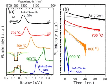
Figure 1共a兲 shows the PL spectra for the as-grown and the annealed QD samples measured at 10 K under a low excitation power of 0.5 mW. The PL spectrum for the type-I InAs/GaAs QDs is also shown for comparison. With the in-creasing TA, a blueshift and a narrowing of the QD’s emis-sion peak were observed.12–17The energy blueshift is caused by the alloy intermixing between the QDs and barrier mate-rials, which shallows the QD’s confining potential due to the
a兲Author to whom correspondence should be addressed. Electronic mail: [email protected]. 0 20 40 60 80 PL Int ens ity (a.u. ) Time ( ns ) InAs/GaAs QDs 900oC 800oC 700oC As grown (a) As grown 700oC 900oC 800oC InAs/GaAsSb QDs (b) InAs/GaAs QDs 17001500 1300 1100 900 0.7 0.8 0.9 1.0 1.1 1.2 1.3 PL in te ns ity ( a. u. ) Energy ( eV ) Wavelength ( nm ) x2 x3
FIG. 1. 共Color online兲 PL spectra 共a兲 and TRPL decay traces 共b兲 for the as-grown and annealed InAs/GaAsSb QDs, together with the reference InAs/GaAs QDs.
APPLIED PHYSICS LETTERS 94, 053101共2009兲
0003-6951/2009/94共5兲/053101/3/$25.00 94, 053101-1 © 2009 American Institute of Physics This article is copyrighted as indicated in the article. Reuse of AIP content is subject to the terms at: http://scitation.aip.org/termsconditions. Downloaded to IP:
incorporation of more Ga atoms into the InAs QDs.12–17For the as-grown sample, it has been confirmed in our previous study7that the InAs/GaAs0.84Sb0.16QDs exhibited a type-II band lineup, where the radiative recombination occurs be-tween the electrons confined in the QDs and the holes in the GaAsSb layer. Annealing induced alloy intermixing also tends to smooth the VB discontinuity at the InAs–GaAsSb interface. Therefore, the electron-hole wave function over-laps and hence the radiative recombination rate is expected to be enhanced or even changed gradually to type-I transi-tions after thermal annealing.
To understand the effects of thermal annealing on the recombination dynamics in the type-II QDs, TRPL measure-ments have been performed and the results are shown in Fig. 1共b兲. The PL decay time was found to decrease with the increasing TA, indicative of a more penetrated hole wave function into the InAs QDs due to the reduced VB offset caused by alloy intermixing at the InAs–GaAsSb interface. In particular, we found that the decay transient for the 900 ° C annealed QDs became as fast as the InAs/GaAs type-I QDs. This implies that the QD structure has been changed to a type-I band alignment after high-temperature annealing.
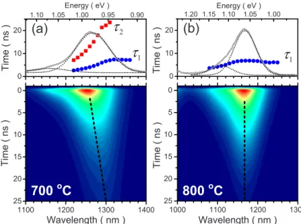
In principle, the recombination lifetime can be quantita-tively deduced from the measured PL decay transients. How-ever, the determination of recombination lifetime is not straightforward for a type-II system. One complication arises from the effect of nonequilibrium carriers: as the carriers recombine continuously, the PL shifts to lower energies due to the reduced VB bending surrounding the QDs.3–10 There-fore, the decay transient recorded at a given wavelength does not reflect the true lifetime since the PL decay arises not only from the carrier recombination but also from the temporal PL shift. For the InAs/GaAsSb material system, the carrier dy-namics is further complicated by the presence of localized hole states in the GaAsSb layer due to alloy fluctuations and/or Sb clustering.7 The redistribution of holes among these localized states also significantly influences the overall carrier dynamics, particularly at low temperatures.7In order to clarify the role of both effects 共i.e., the nonequilibrium carriers and the localized states兲 in the PL transients, energy dependent TRPL has been performed. The results for the 700
and 800 ° C annealed QDs are shown in Figs.2共a兲and2共b兲, respectively. For the 700 ° C annealed QDs, a clear temporal PL redshift can be observed. Since the excitation power was kept low, the effect of nonequilibrium carriers is expected to be less significant. In fact, an even more pronounced tempo-ral PL shift was observed for the as-grown sample. Thus we ascribe the temporal PL redshift to the effect of hole local-izations in the GaAsSb layer. On the contrary, the temporal PL redshift was absent for those QDs annealed at TA ⱖ800 °C. This indicates that the localized hole states have been removed by the annealing induced alloy intermixing. The temporal PL redshift is closely related to the nonsingle-exponential decay observed in PL transients shown in Fig. 1共b兲. Investigations of all samples revealed that the temporal PL redshift can be observed only when the decay transient is nonsingle exponential. By using a double exponential func-tion I共t兲=A1e−t/1+ A
2e−t/2 to fit the PL decay recorded at each wavelength, the decay time constants1 and2 for the faster and the slower decay components can be obtained. The fitted results are shown in the upper panel of Fig. 2, along with its time integrated PL spectrum. For the 700 ° C an-nealed QDs, both1and2show strong energy dependences, indicative of hole transfers among localized states in the GaAsSb layer.7For the 800 ° C annealed QDs, we found that
1 is almost unchanged across the ground state emission band.
The energy dependent lifetime can be described by
共E兲=rad/兵1+exp关共E−Eme兲/E0兴其, whereradis the radiative lifetime, E0 describes the localization depth, and Eme is the energy similar to the mobility edge.18 Figure 3 shows the radiative recombination rate 共rad−1兲 deduced from the energy dependent lifetime for all annealed samples. The measured
rad−1 increases slightly from 0.095 ns−1 for the as-grown sample to 0.15 ns−1 after annealing at TA= 800 ° C, but still about an order of magnitude lower than the InAs/GaAs type-I QDs 共1.25 ns−1兲. The low recombination rates indi-cate that their band lineups remain type-II, with an electron-hole wave function overlap of only ⬃28%–35% of the type-I QDs. As TA was increased to 900 ° C, the recombina-tion rate increases dramatically to rad−1= 1.2 ns−1, which is 0 10 20 1.10 1.05 1.00 0.95 0.90 1100 1200 1300 1400 25 20 15 10 5 0 Wavelength ( nm ) Ti me ( ns ) Time ( ns ) Energy ( eV ) 0 10 20 1.20 1.15 1.10 1.05 1.00 1000 1100 1200 1300 25 20 15 10 5 0 Wavelength ( nm ) Ti me ( ns ) Tim e ( ns ) Energy ( eV )
700
oC
800
oC
(a)
(b)
1τ
2τ
1τ
FIG. 2. 共Color online兲 Energy dependent carrier life-times and time evolution of the PL spectra for the samples annealed at共a兲 700 °C and at 共b兲 800 °C.
053101-2 Liao et al. Appl. Phys. Lett. 94, 053101共2009兲
This article is copyrighted as indicated in the article. Reuse of AIP content is subject to the terms at: http://scitation.aip.org/termsconditions. Downloaded to IP: 140.113.38.11 On: Wed, 30 Apr 2014 15:30:39
very close to that of the type-I QDs, and confirms the band alignment change after annealing.
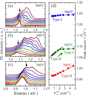
In order to examine whether the QDs are still present after high-temperature annealing, rather than evolving into a quantum-well-like structure, we have also measured the power-dependent PL spectra for the annealed samples. Fig-ure4shows a comparison among the power-dependent spec-tra for the QDs annealed at 700, 800, and 900 ° C. With the increasing excitation power 共Pex兲, higher energy peaks be-come observable for all samples due to the state-filling ef-fect, which is a feature specific to a zero-dimensional system.13,15–17This demonstrates unambiguously that the an-nealed structures remain as QDs even after 900 ° C anneal-ing. The peak energy shifts in the power-dependent spectra also provide evidences for the band alignment changes after thermal annealing. For the 700 ° C annealed QDs, the QD peaks shift linearly with Pex1/3, i.e., a fingerprint of type-II transitions.3 This feature is not observed for the QDs an-nealed at 900 ° C, confirming their type-I alignment. The most interesting is the case annealed at 800 ° C, where the peak blueshift is observed at lower excitation powers but becomes nearly unchanged for Pex⬎5 mW. This behavior can be explained by an evolution from the type-II to type-I recombination induced by the large VB bending surrounding
the QDs. After 800 ° C annealing, the VB offset at the InAs-GaAsSb interface has been reduced by the alloy inter-mixing. To confine holes around the QDs and retain a type-II recombination, the VB bending should be weak and the ex-citation power must be low. When a large amount of non-equilibrium electrons was injected into the QDs by a higher
Pex, a very strong VB bending will exhibit in the QD sur-rounding. This makes the small VB offset unable to support confined hole states in the QD surrounding, leading to a gradual evolution from a type-II to a type-I transition.
In summary, the emission properties of the InAs/GaAs1−xSbxtype-II QDs after thermal annealing have been investigated. Apart from large blueshifts and a pro-nounced narrowing of the QD emission peak, alloy intermix-ing also lead to enhanced recombination rates and reduced localized states in the GaAsSb layer. The type-II QD struc-ture has evolved into a type-I alignment after 900 ° C anneal-ing. We found that it is possible to manipulate between type-I and type-II recombinations in annealed QDs by using differ-ent excitation powers. We demonstrated that postgrowth an-nealing can be used to tailor the band alignment, the wave function overlaps, and hence the recombination dynamics in the InAs/GaAsSb type-II QDs.
This work was supported in part by the project of MOE-ATU and the National Science Council of Taiwan un-der Grant No. NSC 97-2112-M-009-015-MY2.
1H. Y. Liu, M. J. Steer, T. J. Badcock, D. J. Mowbray, M. S. Skolnick, P. Navaretti, K. M. Groom, M. Hopkinson, and R. A. Hogg,Appl. Phys. Lett. 86, 143108共2005兲.
2J. M. Ripalda, D. Granados, Y. Gonzalez, A. M. Sanchez, S. I. Molina, and J. M. Garcia,Appl. Phys. Lett. 87, 202108共2005兲.
3C. Y. Jin, H. Y. Liu, S. Y. Zhang, Q. Jiang, S. L. Liew, M. Hopkinson, T. J. Badcock, E. Nabavi, and D. J. Mowbray,Appl. Phys. Lett. 91, 021102
共2007兲.
4W.-S. Liu, D. M. T. Kuo, J.-I. Chyi, W.-Y. Chen, H.-S. Chang, and T. M. Hsu,Appl. Phys. Lett. 89, 243103共2006兲.
5P.-C. Chiu, W.-S. Liu, M.-J. Shiau, J.-I. Chyi, W.-Y. Chen, H.-S. Chang, and T.-M. Hsu,Appl. Phys. Lett. 91, 153106共2007兲.
6Y. D. Jang, T. J. Badcock, D. J. Mowbray, M. S. Skolnick, J. Park, D. Lee, H. Y. Liu, M. J. Steer, and M. Hopkinson,Appl. Phys. Lett. 92, 251905
共2008兲.
7W.-H. Chang, Y.-A. Liao, W.-T. Hsu, M.-C. Lee, P.-C. Chiu, and J.-I. Chyi,Appl. Phys. Lett. 93, 033107共2008兲.
8U. E. H. Laheld, F. B. Pedersen, and P. C. Hemmer,Phys. Rev. B52, 2697 共1995兲.
9C.-K. Sun, G. Wang, J. E. Bowers, B. Brar, H.-R. Blank, H. Kroemer, and M. H. Pilkuhn,Appl. Phys. Lett. 68, 1543共1996兲.
10F. Hatami, M. Grundmann, N. N. Ledentsov, F. Heinrichsdorff, R. Heitz, J. Böhrer, D. Bimberg, S. S. Ruvimov, P. Werner, V. M. Ustinov, P. S. Kop’ev, and Zh. I. Alferov,Phys. Rev. B 57, 4635共1998兲.
11R. B. Laghumavarapu, A. Moscho, A. Khoshakhlagh, M. El-Emawy, L. F. Lester, and D. L. Huffaker,Appl. Phys. Lett. 90, 173125共2007兲.
12R. Leon, Y. Kim, C. Jagadish, M. Gal, J. Zou, and D. J. H. Cockayne,
Appl. Phys. Lett. 69, 1888共1996兲.
13S. Malik, C. Roberts, R. Murray, and M. Pate,Appl. Phys. Lett.71, 1987 共1997兲.
14S. J. Xu, X. C. Wang, S. J. Chua, C. H. Wang, W. J. Fan, J. Jiang, and X. G. Xie,Appl. Phys. Lett. 72, 3335共1998兲.
15R. Leon, S. Fafard, P. G. Piva, S. Ruvimov, and Z. Liliental-Weber,Phys.
Rev. B 58, R4262共1998兲.
16S. Fafard and C. Nì. Allen,Appl. Phys. Lett. 75, 2374共1999兲. 17T. M. Hsu, Y. S. Lan, W.-H. Chang, N. T. Yeh, and J.-I. Chyi,Appl. Phys.
Lett. 76, 691共2000兲.
18S. F. Chichibu, T. Onuma, T. Sota, S. P. DenBaars, S. Nakamura, T. Kitamura, Y. Ishida, and H. Okumura,J. Appl. Phys. 93, 2051共2003兲.
QW QD InAs/GaAs Type-I QDs Type-II Type-I 500 600 700 800 900 0.1 1 10 Rat e ( ns -1 ) Annealing temperature (o C )
FIG. 3.共Color online兲 Radiative recombination raterad−1as a function of the annealing temperature. The data from the as-grown sample are plotted at 500 ° C. 0 1 2 3 4 5 0.95 1.00 1.05 1.10 1.15 1.20 1.25 1.30 1.1 1.2 1.3 1.4 1.5 1.0 1.1 1.2 1.3 0.8 0.9 1.0 1.1 1.2 Energy ( eV ) P1/3ex (mW1/3) 700oC 800oC 900oC PL intens ity ( a. u. ) Pe ak ene rgy (e V) 900oC 800oC 700oC (a) (b) (c) (d) Type-I Type-II Type-II Type-I
FIG. 4.共Color online兲 Power dependent PL spectra for the samples annealed at共a兲 900 °C, 共b兲 800 °C, and 共c兲 700 °C. 共d兲 The peak energy of QD ground state as a function of Pex1/3.
053101-3 Liao et al. Appl. Phys. Lett. 94, 053101共2009兲
This article is copyrighted as indicated in the article. Reuse of AIP content is subject to the terms at: http://scitation.aip.org/termsconditions. Downloaded to IP: 140.113.38.11 On: Wed, 30 Apr 2014 15:30:39