are subject to the ESD test. It is found that the contact resistance of the TFTs, instead of the channel quality, dominates the ESD power for them to be damaged.
Index Terms—Amorphous Indium–Gallium–Zinc Oxide thin
film transistor (a-IGZO TFT), electrostatic discharge (ESD). I. INTRODUCTION
A
MORPHOUS Indium–Gallium–Zinc Oxide (a-IGZO)thin-film transistors (TFTs) have attracted more attention as one of promising candidates for next generation active matrix flat-panel displays driving element owing to their high mobility, excellent uniformity, and good applicability for low-temperature process [1]–[5]. Since the TFTs are fabricated on the glass substrates in the most applications, the electrostatic discharge (ESD) [6] is an important issue for the fabrication and reliability [7]. TFT LCDs are built from a multi-layer structure on a glass substrate to the whole product module. Most of the processes in the production combine movement, separation and friction. The different ESD types could happen in the production process. For example, some process of the friction may cause the mechanical mode (MM) ESD. The assembly process of glass and driving board may cause the chip-level charge device model (CDM) ESD [8], [9]. Besides, any movement with the human contact may cause the human body mode (HBM) ESD [10].
The transmission line pulsing (TLP) system is commonly used for CMOS device level ESD robustness testing in Inte-grated Circuits (ICs) is applied in this paper to simulate HBM ESD event [11]. There are a few papers using TLP to study the ESD issues of amorphous and polycrystalline silicon TFTs [12]–[20]. However, there is yet no related report regarding the effect of ESD on a-IGZO TFTs. In this work, the ESD robust-ness of a-IGZO TFTs in the connection of the diode-connected Manuscript received August 03, 2012; revised February 26, 2013; accepted April 05, 2013. Date of publication May 02, 2013; date of current version August 07, 2013.
Y.-H. Tai is with the Department of Photonics & Display Institute, National Chiao Tung University, Hsinchu 30010, Taiwan (e-mail: [email protected]. tw).
H.-L. Chiu and L.-S. Chou are with the Department of Photonics & Institute of Electro-Optical Engineering, National Chiao Tung University, Hsinchu 30010, Taiwan (e-mail: [email protected]; [email protected]).
Color versions of one or more of the figures are available online at http:// ieeexplore.ieee.org.
Digital Object Identifier 10.1109/JDT.2013.2257680
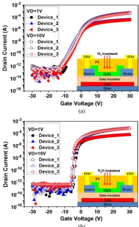
Fig. 1. – transfer characteristics of a-IGZO TFTs with treatment of (a) O and (b) N O and their correspondent cross-section schematics.
type with different W/L fabricated on glass substrate is eval-uated by the TLP measured secondary breakdown current (It2) and the breakdown voltage corresponding to it [21], [22]. Moreover, the ESD effects on the different a-IGZO TFTs with O and N O treatment are discussed.
II. DEVICEFABRICATION
The experimental work was based on the bottom-gate TFT devices of co-planar structure with symmetrical Source/Drain (S/D) fabricated on the glass substrate. Shaped Ti/Al/Ti (50/200/50 nm) gate electrodes were capped with 400-nm-thick SiNx gate dielectric, which was deposited by plasma enhanced chemical vapor deposition (PECVD) at 370 C. The S/D metals were deposited by DC sputtering system at room temperature with Ti/Al/Ti (50/200/50 nm). Then active layer of 30-nm-thick a-IGZO film was deposit by DC magnetron sputtering system
using a target of In Ga Zn in atomic ratio with
the O Ar ratio about 7%. Both N O and O treatments were conducted by PECVD at 170 C with 1500 mTorr for 20 s after 1551-319X © 2013 IEEE
614 JOURNAL OF DISPLAY TECHNOLOGY, VOL. 9, NO. 8, AUGUST 2013
Fig. 2. – transfer curves evolution with gate bias stress for the devices with (a) O treatment and (b) N O treatment.
the formation of IGZO thin film to obtain the different electrical characteristics for the later discussions in comparison. Both treatments were conducted at the same chamber where to form the passivation without breaking the vacuum.
After that, the devices are capped with 100 nm thick SiOx at 200 C as protection layer to avoid the disturbance of outside surrounding. Then the via holes and ITO were patterned and shaped for device measurement. The final annealing step was conducted at 330 C for 2 hours in the oven. The electrical char-acteristics are measured by Agilent 4156-C system at 25 C in dark under 1 atmosphere pressure. The threshold voltage is defined by the gate voltage when the size-normalized drain current reaches 10 A. The subthreshold swing (S.S) and effective field mobility are extracted at drain voltage
V.
III. DEVICECHARACTERISTICS
Fig. 1 shows the cross section and initial transfer character-istics of fabricated devices with the two different treatments. The values of , and S.S for the devices with N O treat-ment are 3.93 V, 18.13 cm V s, and 0.88 V/dec, accordingly, while those for O treated samples are 2.29 V, 10.32 cm V s, and 1.77 V/dec, correspondingly. It can be seen that the devices with N O treatment have better electrical performance than O treated devices do. The worse initial electrical characteristics of O treated device may come from the reason that the O treat-ment is a process which can generate the n-type oxygen vacan-cies to increase the conductivity of the device back channel as the situation in ZnO TFTs [23].
Fig. 3. shift versus stress time under NBS and PBS.
Fig. 4. Configuration of TLP system used in this paper.
For the electrical stability, the two kinds of device with dif-ferent treatment were stressed with positive bias stress (PBS) of 30 V and negative bias stress (NBS) of 30 V separately. Fig. 2(a) and (b) shows the – curves of the devices with different treatments before and after stress 1500 s. The trends of shifting value versus time for the two kinds of devices under PBS and NBS are shown in Fig. 3. It is shown that de-vices with N O treatment have better electrical stability than devices with O treatment during the DC stress. The stress re-sult is quite consist with previous report that devices with N O treatment have better electrical stability [24]–[26] owing to the effect of repairing of device back channel defect [27], [28].
IV. ESD TESTING ANDRESULTS
The configuration of TLP system is shown in Fig. 4 [11]. In this work, the diode-connected IGZO TFTs of different width/ length (W/L) with grounded source node are subject to the ESD test as the DUTs. The TLP energy is injected from the gate/drain node to the source node, which means that the diode-connected IGZO TFT is under forward TLP stress. The failure criterion is defined when the permanent damage is observed to cause open characteristic on the TFT or the abnormal turn on resistance is observed on the TLP-measured – curve. At this moment, the device is expected to be permanently damaged. Fig. 5(a) shows the TLP system measurement results of the DUTs. One pair of It2 and is indicated for the better illustration. One of the – curves for the damaged TFT is shown in Fig. 5(b) and
Fig. 5. TLP system measured – curves of the a-IGZO TFTs. (b) One of the TLP system measured device’s – transfer curve before and after ESD testing.
compared to its initial characteristic to convince the failure of the device.
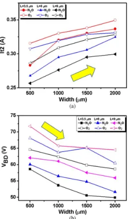
Fig. 6(a) and (b) shows the dependence of the TLP-measured It2 and of several diode-connected devices, correspond-ingly. It is found that with increasing W, the value of It2 gets higher while the becomes lower. On the other hand, with increasing L, the value of It2 becomes lower while the be-comes higher, as shown in Fig. 7(a) and (b), respectively. It is further observed that the It2 of O -treated devices are always higher than the N O-treated devices. Fig. 8 plots the multipli-cation of It2 and , which reflects the breakdown power of ESD for the devices with different W/L. Obviously, the devices with O treatment can sustain higher ESD power than those with N O treatment. It hints that there might be a common mecha-nism resulting in the difference of the treatment effect on the devices in both ESD robustness and performance.
V. ANALYSIS
The optical microscopic (OM) observation and scanning electron microscopic (SEM) graphs of the device damaged by ESD testing are shown in Fig. 9. It is observed that the apparent damage happens not only in the channel but also the contact region, which seems even more damaged.
Fig. 10 illustrates the layout of the TFT testkey and the X marks which denote that the possible weak spots randomly dis-tributed along the width. In the way of layout, the contact area scales with W. If these spots burned out at the very same mo-ment, the ESD power should increase with W for the more
Fig. 6. (a) It2 and (b) versus W for the same L.
Fig. 7. (a) It2 and (b) versus L for the same W.
breakdown area. However, as shown in Fig. 8, the ESD power is independent of W. It depicts that it is the first breakdown of the weakest spot dominates the ESD power where and It2
616 JOURNAL OF DISPLAY TECHNOLOGY, VOL. 9, NO. 8, AUGUST 2013
Fig. 8. ESD power for the devices with different W/L.
Fig. 9. OM and SEM observation of the device after the ESD testing.
Fig. 10. Possible weak spots on the layout of the TFT testkey.
happen. After that, the measured TLP current corresponding to the larger TLP voltage pulse is no more significant since the de-vice has already been damaged.
On the other hand, the contact design for the device with dif-ferent L is identical. It leads us to think that the ESD power may be more related to the contact region than the channel region, which is consistent with the OM and SEM. Thus, we further an-alyze the devices with different treatments in the aspect of the contact resistances.
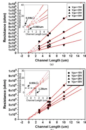
The parasitic contact resistances [29]–[31] are extracted by
the measurement of curves at V with
dif-Fig. 11. Parasitic resistance extraction for a-IGZO TFTs of (a) O treatment and (b) N O treatment.
ferent channel length [32]–[34], where the ON resistance of TFT is represented as (1)
(1) where is the channel resistance per unit channel length, and denote the source and drain resistance, respectively. With the field-effect mobility , the gate insulator unit capac-itor , and the threshold voltage , can be represented as (2)
(2) By substituting (2) into (1), the contact resistances
of TFTs with different treatment can be extracted, as shown in Fig. 11. The extraction results of the contact resistance for the TFTs with O and N O treatment are 0.588 K and 6.88 K , respectively. The devices with N O treatment have much higher contact resistance than those with O treatment.
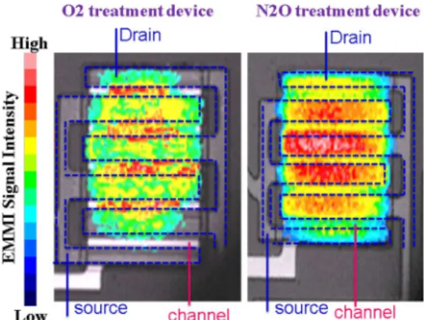
It implies that the contact resistance plays a role in the ESD robustness. The Emission Microscope (EMMI/InGaAs) obser-vation of the devices under the gate bias of 40 V and drain bias of 20 V is further conducted to check the heat distribution. Fig. 12 shows the heat distribution of devices with O and N O treat-ments on the left and right, respectively. It is found that the hottest area of the N O treated device is around the contact area, while that in the O treated device is around the channel.
Such difference depicts that the current dissipates around con-tact area may be larger than the devices with lower concon-tact re-sistance under the same applied G/D voltages. Even with better
Fig. 12. EMMI/InGaAs observation of the devices with (a) O treatment and (b) N O treatment under gate bias of 40 V and drain bias of 20 V.
performance and stability, the device having higher contact re-sistance can be less robust to ESD. Since the only differences between the two kinds of devices are the channel and contact resistances, we come to a conclusion that the contact resistance is the dominate factor that affects the ESD robustness.
VI. CONCLUSION
In this work, the ESD robustness of the diode-connected IGZO TFT is studied by the wafer level TLP testing. The experiment result shows that the ESD protection ability of the co-planar type diode-connected device varies with different W/L, while the multiplication of breakdown voltage and the It2 is constant. This multiplication value is corresponding to the ESD power and mainly affected by the contact resistance, instead of the active area quality. Even with the worse device performance, the devices having the lower contact resistance may sustain higher applied ESD testing voltage.
REFERENCES
[1] N. L. Dehuff, E. S. Kettenring, D. Hong, H. Q. Chiang, J. F. Wager, R. L. Hoffman, C. H. Park, and D. A. Keszler, “Transparent thin-film transistors with zinc indium oxide channel layer,” J. Appl. Phys., vol. 97, no. 6, p. 064505, 2005.
[2] H. Q. Chiang, J. F. Wager, R. L. Hoffman, J. Jeong, and D. A. Keszler, “High mobility transparent thin-film transistors with amorphous zinc tin oxide channel layer,” Appl. Phys. Lett., vol. 86, no. 1, p. 013503, 2005.
[3] M. Fryer, E. C. Colgan, E. Galligan, W. Graham, R. Horton, L. Jenkins, R. John, Y. Kuo, K. Latzko, F. Libsch, A. Lien, R. Nywening, R. Po-lastre, M. E. Rothwell, J. Wilson, R. Wisnieff, and S. Wright, “Pla-narized copper gate hydrogenated amorphous-silicon thin-film transis-tors for AM-LCDs,” in Mat. Res. Soc. Symp. Proc., 1998, vol. 37, p. 508.
[4] P. M. Fryer, E. C. Colgan, E. Galligan, W. Graham, R. Horton, D. Hunt, K. Latzko, R. Nywening, L. Jenkins, R. John, P. Koke, Y. Kuo, F. Libsch, A. Lien, I. Lovas, R. Polastre, M. E. Rothwell, J. Souk, J. Wilson, R. Wisnieff, and S. Wright, “A six-mask TFT-LCD process using copper-cate metallurgy,” in SID Dig. Tech. Papers, 1996, p. 333. [5] H. Sirringhaus, S. D. Theiss, A. Kahn, and S. Wagner, “Self-passivated copper gates for amorphous silicon thin-film transistors,” IEEE
Elec-tron Device Lett., vol. 18, no. 3, pp. 388–390, Mar. 1997.
[6] J. A. Salcedo, J. J. Liou, and J. C. Bernier, “Design and integration of novel SCR-based devices for ESD protection in CMOS/BiCMOS technologies,” IEEE Trans. Electron Devices, vol. 52, no. 12, pp. 2682–2689, Dec. 2005.
[12] E. Fortunato, L. Pereira, P. Barquinha, A. Rego, G. Goçcalves, A. Vilà, J. Morante, and R. Martins, “High mobility indium free amorphous oxide thin film transistors,” Appl. Phys. Lett., vol. 92, no. 22, p. 222103, 2008.
[13] M. Tada, S. Uchikoga, and M. Ikeda, “Power-density-dependant failure of amorphous Si TFT,” in Proc. AMLCD, 1996, pp. 269–272. [14] H. Q. Chiang, J. F. Wager, R. L. Hoffman, J. Jeong, and D. A. Keszler,
“High mobility transparent thin-film transistors with amorphous zinc tin oxide channel layer,” Appl. Phys. Lett., vol. 86, no. 1, p. 013503, 2005.
[15] D. H. Kim, N. G. Cho, H. G. Kim, and I. D. Kim, “Highly transparent InGaZnO4 thin film transistors using Indium-doped ZnO electrodes on plastic substrate semiconductor devices, materials, processing,”
Elec-trochem. Solid-State Lett., vol. 12, pp. H198–H201, 2009.
[16] T. Yanagisawa, “Electrostatic damage and protection for TFT-LCDs,” in SID Dig. Tech. Papers, 1993, pp. 735–738.
[17] S. Uchikoga, M. Kakinoki, K. Suzuki, and M. Ikeda, “Deterioration mechanism of a-Si:H TFT caused by ESD,” in Proc. AMLCD, 1994, pp. 128–131.
[18] N. T. Golo, F. G. Kuper, and T. J. Mouthaan, “Analysis of the elec-trical breakdown in hydrogenated amorphous silicon thin-film transis-tors,” IEEE Trans. Electron Devices, vol. 49, no. 6, pp. 1012–1018, Jun. 2002.
[19] N. T. Golo, F. G. Kuper, and T. J. Mouthaan, “Transmission line model testing of top-gate amorphous silicon thin film transistors,” in Proc.
IRPS, 2000, pp. 289–294.
[20] S. C. Lee, B. C. Jeon, K. C. Moon, M. C. Lee, and M. K. Han, “Elec-trostatic discharge effects on polysilicon TFTs for AMLCD,” in SID
Dig. Tech. Papers, 2002, pp. 212–215.
[21] B. C. Jeon, S. C. Lee, M. C. Lee, K. C. Moon, J. K. Oh, and M. K. Han, “ESD degradation analysis of poly-Si N-type TFT employing TLP (transmission line pulse) test,” in Proc. EOS/ESD Symp., 2002, pp. 191–196.
[22] J. Barth, K. Verhaege, L. G. Henrry, and J. Richner, “TLP calibra-tion, correlacalibra-tion, standards, new techniques,” in Proc. EOS/ESD Symp., 2000, pp. 85–96.
[23] K. Remashan, D. K. Hwang, S. D. Park, J. W. Bae, G. Y. Yeom, S. J. Park, and J. H. Jang, “Effect of N O plasma treatment on the perfor-mance of ZnO TFTs,” Electrochem. Solid-State Lett., vol. 11, no. 3, pp. H55–H59, 2008.
[24] J. Park, S. Kim, C. Kim, S. Kim, I. Song, H. Yin, K. K. Kim, S. Lee, K. Hong, J. Lee, J. Jung, E. Lee, K. W. Kwon, and Y. Park, “Gate-bias stress in amorphous oxide semiconductors thin-film transistor,” Appl.
Phys. Lett., vol. 93, no. 5, p. 053505, 2008.
[25] E. Fortunato, R. Barros, P. Barquinha, V. Figueiredo, S. K. Park, C. S. Hwang, and R. Martins, “Transparent p-type SnO thin film transistors produced by reactive rf magnetron sputtering followed by low temper-ature annealing,” Appl. Phys. Lett., vol. 97, p. 052105, 2010. [26] C. T. Tsai, T. C. Chang, S. C. Chen, I. Lo, S. W. Tsao, M. C. Hung, J.
J. Chang, C. Y. Wu, and C. Y. Huang, “Influence of positive bias stress on N O plasma improved InGaZnO thin film transistor,” Appl. Phys.
Lett., vol. 96, no. 24, p. 242105, 2010.
[27] M. C. Hung, H. T. Hsiao1, W. T. Lin, C. H. Tu, J. J. Chang, and P.-L. Chen, “Employ present five masks amorphous silicon thin-film transistor design and process flow to realize 5-in. InGaZnO active-ma-trix liquid crystal display with improved stress stability,” Jpn. J. Appl.
Phys., vol. 50, p. 03CB0, 2011.
[28] H. Yim, D. H. Kim, S. C. Choi, B. G. Choi, S. Lee, S. K. Kim, K. S. Park, J. U. Bae, C. D. Kim, M. Jun, and Y. K. Hwang, “Highly stable amorphous indium gallium zinc oxide thin-film transistors with N O plasma treatment,” in SID Dig. Tech. Papers, 2011, vol. 42, no. 1, pp. 1170–1172.
618 JOURNAL OF DISPLAY TECHNOLOGY, VOL. 9, NO. 8, AUGUST 2013
[29] O. Marinov, M. Jamal Deen, U. Zschieschang, and H. Klauk, “Organic thin-film transistors: Part I—Compact DC modeling,” IEEE Trans.
Electron Devices, vol. 56, no. 12, pp. 2952–2961, Dec. 2009.
[30] M. J. Deen, O. Marinov, U. Zschieschang, and H. Klauk, “Organic thin-film transistors: Part II—Parameter extraction,” IEEE Trans.
Elec-tron Devices, vol. 56, no. 12, pp. 2962–2968, Dec. 2009.
[31] M. J. Deen, M. H. Kazemeini, Y. M. Haddara, J. Yu, G. Vamvounis, S. Holdcroft, and W. Woods, “Electrical characterization of polymer-based FETs fabricated by spin-coating poly(3-alkylthiophene),” IEEE
Trans. Electron Devices, vol. 51, no. 11, pp. 1892–1901, Nov. 2004.
[32] J. Kanicki, F. R. Libsch, J. Griffith, and R. Polastre, “Performance of thin hydrogenated amorphous silicon thin film transistors,” J. Appl
Phys., vol. 69, no. 4, pp. 2339–2345, 1991.
[33] S. Luan and G. W. Neudeck, “An experimental study of the source/ drain parasitic resistance effects in amorphous silicon thin film transis-tors,” J. Appl. Phys., vol. 72, no. 2, p. 766, 1992.
[34] J. Jeong, Y. Hong, J. K. Jeong, J. S. Park, and Y. G. Mo, “MOSFET-like behavior of a-InGaZnO thin-film transistors with plasma-exposed source–drain bulk region,” J. Display Technol., vol. 5, no. 12, pp. 495–500, Dec. 2009.
Ya-Hsiang Tai received the B.S. and Ph.D. degrees
in electronic engineering from National Chiao Tung University, Taiwan, in 1990 and 1996, respectively.
He became a member of Industrial Technology Research Institute/Electronics Research & Service Organization and the TFT LCD development as a panel designer. He joined the project of low temperature polycrystalline silicon (LTPS) thin-film transistor (TFT) development in Prime View In-ternational in 2000. In 2001, he entered Toppoly Optoelectronics Corporation, to lead the team of
LTPS TFT LCD panel design. He joined the faculty of National Chiao Tung University in 2003, where he is currently a professor in the Department of Photonics and Display Institute. His current research emphases are in the areas of TFT device physics, active matrix display panel design, and system on panel.
Hao-Lin Chiu received the B.S. degree in electro-physics from National Chiao
Tung University, Taiwan, in 2004, and the M.S. degree in electro-optical engi-neering in National Chiao Tung University, Taiwan, in 2006, where he is now working for his Ph.D. degree.
His current research interests include the sensor and applications of a-Si and a-IGZO TFTs.
Lu-Sheng Chou received the B.S. degree in physics
from National Sun Yat-Sen University, Taiwan, in 2008. He is now working for his Ph.D. degree in electro-optical engineering in National Chiao Tung University, Taiwan. His current research interests include the sensor and applications of a-Si and a-IGZO TFTs.