行政院國家科學委員會專題研究計畫 成果報告
人造電磁材料之特性分析與應用研究
研究成果報告(精簡版)
計 畫 類 別 : 個別型 計 畫 編 號 : NSC 98-2221-E-009-038- 執 行 期 間 : 98 年 08 月 01 日至 99 年 07 月 31 日 執 行 單 位 : 國立交通大學電信工程學系(所) 計 畫 主 持 人 : 黃瑞彬 計畫參與人員: 碩士班研究生-兼任助理人員:許能傑 碩士班研究生-兼任助理人員:劉鴻萬 博士班研究生-兼任助理人員:金正元 報 告 附 件 : 出席國際會議研究心得報告及發表論文 國際合作計畫研究心得報告 處 理 方 式 : 本計畫可公開查詢中 華 民 國 99 年 09 月 08 日
1
A spatial beam splitter consisting of near-zero
refractive index medium
Ruey-Bing Hwang, Neng-Chieh Hsu, and Cheng-Yuan Chin
Abstract—In this paper, we present a metamaterial-based
beam splitter. Such a beam splitter consists of a metamaterial sandwiched by two metallic plates. The metamaterial consists of a three-dimensional (3D) fishnet arranged in a two-dimensional (2D) square lattice. As was well known from Snell’s law, the refracted wave tends to be normal to the interface when the wave is incident from a medium having effective refractive index smaller than unity into the air region. Based on that concept, we properly synthesize the metamaterial with effective refractive index smaller than unity and put a line source embedded in the metamaterial as an excitation, achieving a four-way beam splitter. In addition to the calculation of wave-propagating characteristics in the metamaterial, we also implemented a beam-splitting structure incorporating the property of near-zero refractive index of the metamaterial. The electric-field radiating pattern was measured to identify its spatially beam-splitting characteristics.
Index Terms—Periodic structures, metamaterial, near-zero
refractive index medium, spatial beam splitter.
I. INTRODUCTION
M
ETAMATERIAL is an artificially engineered structure which obtains its properties from its structure rather than directly from its composition. Generally, a metamaterial is synthesized by embedding specific inclusions, for exam-ple, periodic structures, in a host medium. The applications of metamaterial in waveguides and antennas designed were intensively developed [?], [?]. A metamaterial with zero-index was demonstrated to be able to shape the far-field pattern of an antenna embedded within it. Besides, a matched zero-index slab could be used to transform curved wave fronts into planar ones [?]. The metamaterial made up of wire medium has been studied intensively, particularly on its effective refractive index, permittivity and permeability. Specifically, the structure composed of metallic mesh wires, which has very small elec-trical length in the period and wire thickness, can be character-ized as a homogeneous medium with a low plasma frequency [?]. Besides, a dielectric medium embedded with metallic nano-particles and nano-wires has zero effective permittivity, creating band gaps [?]. Moreover, the split ring resonators can result in an effective negative permeability over a microwave frequency band [?]. The first left-handed metamaterial in mi-crowave frequency was developed. Besides, the extraordinary refraction phenomenon was demonstrated [?]. Metamaterials with both negative permittivity and permeability over an over-lapping near-infrared wavelength range were demonstrated to have a low loss negative-refractive-index [?], [?]. A three-dimensional optical metamaterial made up of cascade ’fish-net’ structures was demonstrated to have a negative index existing over a broad spectral ranges [?]. Additionally, some researchers used the effective medium method to consider themetamaterial slab as a uniform medium. The single-mode approximation was employed to mathematically extract the effective parameters using the scattering parameters including the reflection and transmission coefficients of the metamaterial slab [?]. Regarding the metamaterial-based antenna design, a metamaterial consisting of six identical metallic grid with a square lattice embedded in a foam with relative dielectric constant close to unity was designed [?]. They put a monopole source in the middle of the structure and a metal plate on the bottom of structure for controlling the emission of the structure. The experimental and numerical evidence prove that such a metamaterial can modify the emission of an embedded source. Additionally, the epsilon-near-zero metamaterial for tailoring the phase of radiation pattern of arbitrary sources was proposed and analyzed for some canonical geometries [?]. A strongly modulated photonic crystal having an effective refractive index controllable by the band structure was studied [?]. The experimental and numerical evidence proves that such a metamaterial can not only modify the emission of an embedded source but also enhance the gain and directivity [?]. Different from the conventionally used one equipped with circuit-based power divider, in this research we utilize the physics of wave propagating in a metamaterial with near-zero refractive index to achieve the beam splitting characteristics. In the ensuing section, we will demonstrate the structure configu-ration. In section III, the phase relation of the waves supported in the metamaterial medium will be highlighted to explain the beam-splitting characteristics. Additionally, the effective medium approach for extracting the effective parameters, such as permittivity, permeability, refractive index and wave impedance will be carried out. The numerical and measured results of the far-field radiation pattern will be shown and compared to verify the beam-splitting characteristic. Finally, we will conclude this paper with some remarks.
II. STRUCTURECONFIGURATION
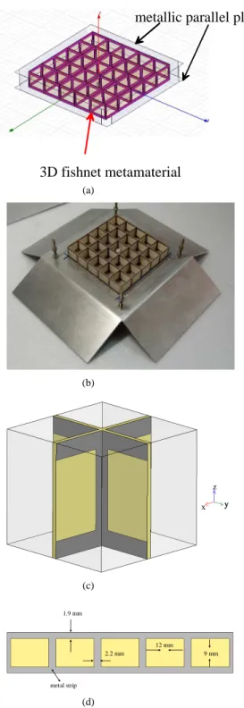
As shown in Fig. 1(a), the structure under consideration comprises a metamaterial sandwiched by two metallic parallel plates. The metamaterial is made up of fishnet structure arranged in a 3D pattern like a jungle gym shown in Fig. 1(b), where the unit cell is depicted in Fig. 1(c). The number of unit cells along the x- and y-direction are both 5. Moreover, the periods (or lattice constant) along the x- and y-direction are denoted asdx(14.2mm) anddy (14.2mm), respectively. Each
row or column of the 3D fishnet structure was constructed by the building block depicted in Fig. 1(d). The mesh wire was printed on the dielectric substrate RO4003 with relative
2
metallic parallel plates
3D fishnet metamaterial (a) (b) z y x z y x (c) 1.9 mm 2.2 mm 12 mm 9 mm metal strip 1.9 mm 2.2 mm 12 mm 9 mm metal strip (d)
Fig. 1. Structure configuration: (a) metamaterial inside metallic parallel plates, (b) photo of the 3D fishnet metamaterial, (c) unit cell of the metama-terial, and (d) front view of the fishnet structure.
dielectric constant 3.55 and thickness 0.508mm using photo lithography and chemical etching process. The dimensions of the metal strip were attached in the figure. Notice that the same pattern was printed on both sides of the dielectric substrate. The metallic parallel plates are made by aluminum with thickness 1.6mm. The distance between the parallel plates is denoted as h (12.8mm). Moreover, a line source made from a coaxial probe was placed in the center of the metamaterial as an excitation source.
III. CHARACTERIZATION OF THE METAMATERIAL
A. Phase Relation
As far as a periodic medium is concerned, the dispersion (or phase) relation of the eigen-wave supported in the medium is an important issue to be studied in detail. Returning to the unit cell of the metamaterial shown in Fig. 1(c), the top and bottom surfaces of the unit cell are perfect electric conductors. Since the metamaterial is regarded as an infinite 2D periodic structure, from the Floquet-Bloch theory the phase differences along the x and y directions are kxdxandkydy, respectively.
After specifying the boundary conditions on the unit cell, we are able to solve the eigen-value problem of the closed structure using finite-element method. Notice that the eigen-value (frequency) obtained corresponds to a propagating mode subject to given phase constants kx and ky. After iterating
the phase constantskxandky, we could determine the phase
relation (the relationship among frequency,kxandky). Figure
2 shows the contour map of the phase relation, the horizontal and vertical axes respectively represent the phase constants (kx
andky) along the x- and y-axis, in the unit of 1/meter. Because
of the symmetry in the unit cell along the x- and y-axis, the phase relation also preserves the symmetry. The circles in colored lines with smaller radius are the phase relation of wave in the metamaterial calculated from 7.2 GHz to 8.0 GHz with 0.2 GHz step, while the circles with larger radius (ko)
are those in the air for reference. Apparently, thenef f of the
wave in the metamaterial is much smaller than that in the air. Notice that below 7 GHz no real frequency was found, it is due to the cutoff phenomenon (plasma-like property) of this structure. 7.2 7.2 7 .4 7.4 7.4 7 .6 7.6 7.6 7.8 7.8 7 .8 7.8 8 8 8 8 kx ky —7.2GHz —7.4GHz —7.6GHz —7.8GHz —8.0GHz -200 -150 -100 -50 0 50 100 150 200 -200 -150 -100 -50 0 50 100 150 200 7.2 7.2 7 .4 7.4 7.4 7 .6 7.6 7.6 7.8 7.8 7 .8 7.8 8 8 8 8 kx ky —7.2GHz —7.4GHz —7.6GHz —7.8GHz —8.0GHz -200 -150 -100 -50 0 50 100 150 200 -200 -150 -100 -50 0 50 100 150 200
Fig. 2. Phase relation of waves propagating in the metamaterial.
The phase relation given above reveals an important infor-mation concerning the propagation of wave at the interface between the metamaterial medium and air. For easy interpre-tation, we assumed that the metamaterial medium and air have the refractive indexnef f and 1.0, respectively. The incident
3
denoted byθi andθtrespectively. From Snell’s law, we know
that the relation between the incident and transmitted angles is given as follow.
nef fsinθi= sinθt (1)
Since nef f < 1, the transmitted angle (θt) must be smaller
than unity. This means that the transmitting wave tends to be perpendicular to the interface between the two media.
B. Effective medium approach for extracting the uniform transmission line parameters
In addition to the calculation of phase relation by solving the eigen-value problem, we have also considered the fishnet structure as an homogeneous slab for retrieving the effective parameters. A robust method was developed [?] using the scattering parameters of a metamaterial slab under normal incidence, from which the effective refractive index n and
normalized impedancez are obtained. Moreover, the effective
permittivity and permeability are calculated fromµ = nz and ǫ = n/z.
Since the metamaterial is a passive medium, the signs of computed z and n must satisfy the requirement
Re{z} ≥ 0 (2)
Im{n} ≥ 0 (3)
and thusz and n can be determined independently by
z = ± s (1 + S11)2− S212 (1 − S11)2− S212 (4) e−jkond = X ± jp1 − X2 (5) n = 1 kod {−[Im{ln(e−jkond )}+2mπ]+j[Re{ln(e−jkond )}]} (6) where X = (1 − S2 11 + S212 )/2S21, S11 and S21
individ-ually represent the reflection- and transmission- coefficient. Parameterskoandd are the free-space wave-number and slab
thickness, respectively.
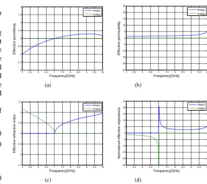
Figures 3 show the retrieved effective parameters using the method described previously, where (a) and (b) respectively are the variation of the effective permittivity and permeability versus frequency, and (c) and (d) individually are those of effective refractive index and normalized impedance, which is normalized to free-space wave impedance 377 Ω. It is
obviously to see that in (a) the plasma-like dielectric function is negative for the operational frequency below 7GHz. Around 7 GHz, the effective permittivity is near zero, while the effective permeability is a positive number. Consequently, before 7 GHz, the wave shall have a pure imaginary num-ber of propagation constant (refractive index) as depicted in (c), exhibiting the below-cutoff phenomenon. Moreover, (d) presents the intrinsic impedance of the wave propagating in the effective medium. Interestingly, the effective refractive index is zero at 7 GHz, however, the impedance is extremely high. Once a wave is excited in the effective medium at 7 GHz,
the high wave-impedance will cause a strong reflection from the interface between the effective medium and air. Generally speaking, when the operation wavelength is greater than the period of a periodic structure, the effective medium method can properly model the complicated structure as a uniform dielectric medium and provide us the uniform transmission line parameters. Thus, the wave propagation through a finite thickness of the structure can be realized.
5 5.5 6 6.5 7 7.5 8 8.5 9 9.5 10 -2 -1.5 -1 -0.5 0 0.5 1 1.5 2 Frequency(GHz) E ff e c ti v e p e rm it ti v it y Real(ε) Imag(ε) (a) 5 5.5 6 6.5 7 7.5 8 8.5 9 9.5 10 -25 -20 -15 -10 -5 0 5 10 15 20 25 Frequency(GHz) E ff e c ti v e p e rm e a b ili ty Real(µ) Imag(µ) (b) 5 5.5 6 6.5 7 7.5 8 8.5 9 9.5 10 -1.5 -1 -0.5 0 0.5 1 1.5 Frequency(GHz) E ff e c ti v e r e fr a c ti v e i n d e x Real(n) Imag(n) (c) 5 5.5 6 6.5 7 7.5 8 8.5 9 9.5 10 -25 -20 -15 -10 -5 0 5 10 15 20 25 Frequency(GHz) N o rm a liz e d e ff e c ti v e i m p e d a n c e Real(z) Imag(z) (d)
Fig. 3. Retrieved constitutive effective parameters of the 3D fishnet metama-terial: (a) permittivity, (b) permeability, (c) refractive index, (d) normalized impedance.
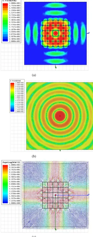
After understanding the phase- and dispersion- relation of eigen-waves supported in the metamaterial, we are now in a good position to observe the physical picture of wave process in the metamaterial medium. In the next example, we numerically simulated the overall structure, particularly for observing its electric-field and Poynting power distribu-tion. By properly tuning the length of the monopole (line source) in the metamaterial, the wave propagating in the medium with effective refractive index smaller than unity was excited. As was predicted previously, the refractive waves shall be normal to the metamaterial surface. To verify this conjecture, we calculated the electric-field distribution and vectorized Poynting power in the parallel-plate region. As shown in Fig. 4(a) and 4(c), the refracted wave leaving the metamaterial medium (highlighted by a grid region) tends to be perpendicular to the metamaterial surface in particular for those around the central part, while the others propagate at a small angle deviated from the normal direction. Additionally, the electric-field distribution for the same structure but without metamaterial was demonstrated for reference. It is apparent to see that without the metamaterial, the wave excited by the monopole propagates outwards like a cylindrical wave, as depicted in Fig. 4(b).
4
(a)
(b)
(c)
Fig. 4. Electric-field strength in the structure with metamaterial (a), and without metamaterial (b); Poynting vector distribution in the structure with metamaterial (c); all the results were evaluated at 7.5 GHz.
C. Radiation Characteristics
In the next example, we demonstrate the spatial power-splitting characteristic of the original structure equipped with flared opening on each of the four output ports, as shown in Fig. 5(a) and 5(b). The radiating far-field patterns along the
X-Y and X-Z plane were measured in an anechoic chamber
using a vector network analyzer (HP 8722D) and standard horn antennas. In this design, the flared opening was employed to enhance the directivity of the original structure. As is well
known in microwave and millimeter wave engineering, the E-plane horn antenna uses a flared opening to taper its dominant waveguide mode from the waveguide end to a large opening while maintaining its field uniformity. Here, the same design was utilized to obtain a uniform electric-field distribution on the flared opening.
(a) z x y z x y (b)
Fig. 5. The top view (a) and side view (b) of the spatial beam-splitting structure.
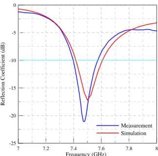
Figure 6 depicts the reflection coefficient against frequency of the structure shown in Fig. 5(b). The vertical- and horizontal- axis individually represents the reflection coeffi-cient (in dB) and frequency (in GHz). The line in blue- and red- color is the measured and calculated result, respectively. From this figure, it is obvious to see that the impedance bandwidth is around 0.2 GHz with VSWR less than 2.
As mentioned previously, the structure under consideration can be employed as a spatial beam splitter. As far as a beam splitter is concerned, the beam pattern should be an important issue to be studied. In the next example, we carry out the numerical simulation for determining the far-field radiation pattern. Specifically, the measured pattern was also plotted for verifying the design concept. As shown in Figs. 7, the red- and blue- color curve represents the measured and simulated pattern, respectively. Figures (a), (c) and (e) are those for X-Y plane, while (b), (d) and (f) are for X-Z
plane. The operational frequency and antenna gain (in dBi) were attached in respective figure. Notice that because of the smaller dimension along the flared-openning direction than the width along x− (or y−) axis the beam pattern has wide
beam-width along the X-Z plane. From these figures, we
may conclude that the four cone-type beam patterns indeed can serve as a spatial beam splitter to distribute the input power to four axes. Significantly, the excellent agreement between the numerical and measured results again confirm the near-zero-index property of the metamaterial utilized in this research. Although not shown in the figures, we have measured the cross-polarization patterns and found that they are much smaller than those of co-polarization.
IV. CONCLUSION
In this paper, an artificial medium based on the 3D fishnet structure was developed. Using the effective medium ap-proach, we regarded the 2D periodic structure as a homo-geneous medium and extracted its effective parameters such as the permittivity, permeability, refractive index and wave impedance. Interestingly, we find that the medium possesses
5 7 7.2 7.4 7.6 7.8 8 Frequency (GHz) -25 -20 -15 -10 -5 0 R ef le c ti o n C o ef fi ci e n t (d B ) Measurement Simulation
Fig. 6. Reflection coefficient (in dB) versus frequency of this spatial beam-splitting structure.
the property of near-zero refractive index. Accordingly, a spatial beam splitter incorporating such a metamaterial was developed to distribute the input power to four ways. To understand the underlying physics of wave process in the metamaterial, the dispersion characteristics of the waves sup-ported by the infinite 2D periodic structure consisting of the unit cell of fishnet structure was analyzed rigorously. Additionally, the Poynting vector and electric-field distribution in the metamaterial medium were demonstrated for verifying the property of near-zero refractive index. Significantly, the excellent agreement between the measured and calculated results confirms the design concept of this research.
0 30 60 90 120 150 180 210 240 270 300 330 -10 -5 0 5 10 Measurement Simulation 7.4 GHz X-Y Plane (Gain=7.85dBi)
(a) 0 30 60 90 120 150 180 210 240 270 300 330 -30 -20 -10 0 10 Measurement Simulation 7.4 GHz X-Z Plane (b) 0 30 60 90 120 150 180 210 240 270 300 330 -10 -5 0 5 10 Measurement Simulation 7.5 GHz X-Y Plane (Gain=8.69dBi)
(c) 0 30 60 90 120 150 180 210 240 270 300 330 -30 -20 -10 0 10 Measurement Simulation 7.5 GHz X-Z Plane (d) 0 30 60 90 120 150 180 210 240 270 300 330 -10 -5 0 5 10 Measurement Simulation 7.6 GHz X-Y Plane (Gain=8.23dBi)
(e) 0 30 60 90 120 150 180 210 240 270 300 330 -30 -20 -10 0 10 Measurement Simulation 7.6 GHz X-Z Plane (f)
Fig. 7. Radiation patterns of the spatial beam-splitting structure on X-Y and X-Z plane.
出席國際會議心得報告
研討會名稱與地點︰2010 Asia-Pacific International Symposium on Electromagnetic Compatibility, Beijing, China, April 12-16
感謝在國科會專題研究計畫的補助下參加2010年在中國北京所舉辦的泛 太平洋國際電磁相容研討會。很榮幸在大會的邀請下擔任該會之
Technical Program Committee委員並且擔任Special Session之主席。本次 會議中,我所發表的論文題目為”Cross-talk suppression using the substrate-integrated waveguide with moats”,基板整合波導(substrate integrated waveguide)之傳播特性與傳統金屬導波管(metallic waveguide) 相似,然而由於其輕薄短小且易於與主動元件結合之特點,近年來已經 逐漸被廣泛使用於毫米波電路與天線系統,具有相當高之系統整合度, 然而也由於其高整合度,substrate integrated waveguides之間的電磁干擾 問題也變成影響系統特性之關鍵因素。本次所發表的論文除了精確分析 產生電磁干擾的物理機制外,並且提出Fabry-Perot resonator的新觀點成 功得解釋電磁耦合原因。重要得是我們利用自行研發之新型substrate integrated waveguide with moats outside the via-hole arrays,獲得相當 好的隔離效果,大幅降低波導間之電磁耦合與干擾。
電磁相容的研究在亞洲逐漸受到重視,過去電磁相容問題在業界大都是 靠著“老師傅“的經驗傳承,缺乏系統性分析,因此對於目前多層印刷 電路板(multilayer printed circuit board)結構可說是束手無策。這次研討 會中,針對印刷電路板系統之電磁干擾問題亦有special session來介紹目 前所使用的各種電磁數值方法在此一問題上之解決方法,個人認為此類 電磁邊界問題太過複雜,欲獲得與實驗一致的結果似乎不可行,因此在 此一領域的研究上還有相當大的發展空間。
附件
Crosstalk suppression using the substrateintegrated
waveguide with moats
Ruey‐Bing Hwang1, Cheng‐Yuan Chin1, Yu‐De Lin1, Toshihide Kitazawa2, and
Chang‐Yu Wu3 1Department of Electrical Engineering, National Chiao Tung University, Hsinchu, Taiwan, R.O.C. 2Department of Electrical and Electronic Engineering, Ritsumeikan University, Kyoto, Japan 3Department of Electronic Engineering, Jinwen University of Science and Technology, Hsin‐Tien City, Taipei County, Taiwan, R.O.C. Abstract
As was well known, the substrate‐integrated waveguide can be easily implemented and integrated with active and passive devices using the printed circuit process. Thus, the integration circuit and system based on the substrate‐ integrated waveguide technique becomes achievable. However, in the integrated circuit environment, the close proximity between adjacent substrate‐integrated waveguides may cause the electromagnetic coupling, and thus the electromagnetic interference problem arises accordingly. In this research, we demonstrate the electromagnetic coupling between two parallel substrate‐ integrated waveguide. Moreover, the theory of Fabry‐Perot resonator was employed to explain the resonance coupling between the substrate‐integrated waveguides. On the other hand, a new substrate‐integrated waveguide equipped with moats [1] was utilized to examine the capability of cross‐talk suppression. Interestingly, we find that in comparison with the conventionally used substrate‐ integrated waveguide the new one can effectively suppress the electromagnetic wave coupling. Therefore, the signal integrity can be further improved in a microwave or millimeter‐wave circuit or system implemented using the substrate‐integrated waveguide technique.
Introduction
Metal waveguides were popular during and after World War II. However, the bulky waveguides were gradually replaced by transmission lines printed on a circuit board, such as micro‐strip line, strip line, coplanar waveguide, slot line, and et. al. Recently, a printed waveguide mimicking the dispersion property of a metal waveguide was successfully developed. Specifically, such a waveguide can be easily fabricated using printed circuit process, and therefore, attracts considerable attentions. It is termed as SIW (substrate‐integrated waveguide) or post‐wall waveguide. This waveguide uses the via‐hole arrays to replace the metallic walls for guiding electromagnetic waves. Besides, since the wave guided in the dielectric substrate with relative dielectric constant larger than that of air, the dimension of the waveguide can be further reduced. Moreover, several transition structures using printed transmission lines were developed to offer a much greater degree of flexibility in practical applications.
Regarding the theoretical investigation relating the guided‐wave and leaky‐wave characteristics of the SIW, various numerical method, such as the finite‐ difference frequency‐domain method [ ], generalized multipole technique [ ], and numerical multimode calibration procedure incorporating the finite‐element method [ ], were developed. In addition to the rigorous full‐wave analysis, the empirical formula for practically design the SIW was also developed. As was indicated in [], the via‐hole array is equivalent to a solid metal wall as the ratio of pitch width to via‐hole radius is smaller than 4 and that of waveguide width to via‐hole radius is greater than 8.
In addition to the commonly used SIW, a new type of SIW by adding moat (slit) outside the via‐hole array [JEMWA] was developed. From the measured scattering parameters and calculated dispersion relation, it is apparent to see that the new structure can maintain an excellent guiding characteristic but using a sparser via‐hole array compared with the conventionally used one. Besides, the cutoff frequency can be reduced to broaden its operational bandwidth.
Incidentally, since numerous microwave and millimeter‐wave components, such as filter, resonator, multiplexer, and even slotted antennas, have been designed based on the SIW, the integration of SIW‐based components and circuit in a printed circuit board becomes an option for microwave circuit and system. However, as far as the integration is concerned, the electromagnetic coupling between lines in close proximity shall be a problem. To evaluate the electromagnetic coupling between SIWs, the two parallel and identical SIWs (like a coupler) were implemented on a printed circuit board to measure its coupling coefficient. It is interesting to observe that the resonance coupling occurs in the structure and, moreover, the coupling strength does not decrease as the separation distance between the two SIWs increases. As will become clear later on, the region bounded by the two SIWs can be regarded as a Fabry‐Perot resonator for contributing the resonance coupling.
Structure configuration
Figure 1 depicts the structure configuration to be analyzed and measured in this research. As shown in this figure, two adjacent and co‐parallel SIWs were fabricated in a microwave dielectric substrate RO4003 with relative dielectric constant 3.55. Each of the SIWs was fed by a micro‐strip line with tapering transitions at its both ends. The via‐hole radius, pitch width between adjacent via‐hole, moat width, and channel width of the waveguide are denoted by r, p, w and a, respectively. Parameter d represents the separation distance between the two SIWs.
Electromagnetic coupling between SIWs and a strategy for crosstalk reduction
From the results reported in [1], we may clearly observe that the moats can further suppress the electromagnetic‐wave leakage from the via‐hole array. Intuitively, such a new waveguide may mitigate the electromagnetic wave coupling between two adjacent and co‐parallel waveguides.
In the following example, we fabricated two SIW circuits with and without moats, respectively, shown in Fig. 1. Each of which contains two SIWs separated by the same distance d. The structure parameters were attached in the figure caption for easy reference. It is noted that the pitch width in the two cases both
are 1 mm, which was designated based on the criterion reported in the literature [K. Wu]. Figure. 2 and 3 demonstrate the scattering parameters including the transmission‐ and coupling‐ coefficients for the coupled SIWs with and without moats, where Fig. 2 and Fig. 3 are simulated‐ and measured‐ result, respectively. The numerical simulation was based on the Time‐Domain Finite‐Integration Method [CST].
From Fig. 2 and 3, it is obvious to see that the coupling coefficient (S31) is significant although the via‐hole array is dense enough. Specifically, there are spikes present in both the simulated and measured results. Although not shown in this paper, we have change the separation distance between the two waveguide to measure its coupling coefficient. From the coupled‐wave theory, we know that if the coupling is due to the evanescent wave outside the waveguide, the coupling coefficient decreases as the separation distance increases. However, those spikes are still present and do not decrease with the increase in the separation distance. We were inspired by this phenomenon to study the coupling mechanism between the SIWs. The electric field (strength of the Ez component) distributions at each resonant frequency in the SIWs were calculated. However, due to the page limitation only the case for the second resonant frequency was shown in Fig. 5. From this figure, it is apparent to see the resonant mode occurring in the region between the two waveguides. In the presence of the two via‐hole arrays, the electric field distribution along the transverse plane resembles that of TE10 mode in the SIW. Moreover, the two open ends cause a standing wave along the x axis. Therefore, the electric‐field distribution exhibits a resonance mode shown in the figure. It may be concluded that the resonance coupling is mainly due to the wave leaky from the first SIW, penetrating through the via‐hole array into the Fabry‐Perot resonator, and finally coupling to the second SIW. Thus, the resonant frequency can be correctly predicted by the formula given below. € f ≈ c 2π εr mπ l 2 + nπ w 2 where l and w are the length and width of the cavity, c is the light speed, and m and n are integers representing mode indices along the x and y‐ axis, respectively. Since the cavity height (substrate thickness) is much smaller than those of the other two dimensions, the fields along the thickness direction can be assumed to be uniform and the formula can be simplified as (1).
We have checked the resonant frequencies based on (1) and found they are caused by the cavity resonance. The three resonant frequencies corresponds to the three resonant modes (m=0, n=1), (m=1, n=1), and (m=1, n=2), respectively. Additionally, from equation (1), we may conjecture that the resonance coupling will start at a lower frequency as the separation distance increases. It was confirmed by the numerical and measured results to be demonstrated in our presentation.
On the contrary, the resonance coupling does not occur in the case of SIWs with moats. Owing to the excellent confinement of the electromagnetic fields in the new SIWs, the cavity modes are hard to be excited and the electromagnetic coupling can be further suppressed.
In this paper, we numerically and experimentally examined the electromagnetic coupling between two SIWs that are close to each other. It is interesting to find that the coupling is considerable even the via‐hole is dense enough. Through a systematical investigation in the electric field distribution, we may conclude that such a coupling is caused by the excitation of resonant modes in the cavity between the two SIWs. In addition to the demonstration for the electromagnetic coupling taking place in conventionally used SIWs, we also provide a strategy for suppressing the coupling by adding moats outside the via‐hole array. The excellent performance in preventing the wave leakage from the waveguide effectively removes the path of electromagnetic interference.
日本立命館大學國際合作心得報告
非常感謝在國科會的國際合作經費補助下與日本立命館大學Professor Kitazawa 共同完成substrate integrated waveguide之研究,此次國際合作之成果豐碩,除了 應邀演講之外,並且與substrate integrated waveguide的發明人Professor Ke Wu做 相關結構之電磁傳波特性討論,對於該結構未來之廣泛應用性有更進一步之了 解。據了解在加拿大,吳教授以將此一結構推廣至THz上,結合毫米波與 THz 波段上的各種應用,未來substrate integrated waveguides circuit將可以整合成為系 統晶片,成為下一世代整合毫米波晶片之標準。 2009年11月7日︰搭機前往日本立命館大學 2009年11月8日︰於立命館大學整理演講資料以及準備會議論文所需之理論分析 結果 2009年11月9日︰參觀日本立命館大學Prof. Kitazawa實驗室以及立命館大學南草 津校區 2009年11月10日︰於立命館大學演講“電磁波於印刷電路板類金屬波導中之傳 波特性分析“,並與substrate integrated waveguide發明人Prof. Ke Wu討論歐洲在 此種新型波導結構上之進展。Prof. Ke Wu除了發明此一結構外,他對於將該結 構推廣至millimeter wave以及terahertz頻段上的應用相當積極,結合主動元件與 該傳輸結構,他預言該結構將成為terahertz積體電路之標準製程。
2009年11月11日︰與Prof. Kitazawa討論substrate integrated waveguides之應用領域 與該結構中電磁場特性,Prof. Kitazawa之研究專長為spectral domain analysis,我 個人則為mode-matching analysis,我們同時利用個別之研究方法進行該波導結構 之色散曲線分析,獲得一致之結果,並完成結果比對工作。證實我們所發展之 理論正確性。
2009年11月12日︰與立命館大學特聘教授Prof. Kikuo Wakino (senior executive director, Murata Manufacturing Co. )見面並討論陶瓷基板材料在substrate integrated waveguide上之應用可行性以及可能面臨之製作瓶頸。
2009年11月13日︰與Prof. Kitazawa研討撰寫論文“Electromagnetic Coupling in Substrate-Integrated Waveguides Circuit and Its Suppression Technique“,該論文由 我們雙方共同撰寫於 Asia-Pacific Electromagnetic Compatibility Conference 2010, 且已由我於2010年四月於中國北京之研討會上發表。
2009年11月14日︰在Prof. Kitazawa的邀請與安排下參觀立命館大學京都校本部 以及京都市
Invited Talk on the topic “Wave Propagating Characteristics in a Substrate Integrated Waveguide with Moats” Department of Electrical and Electronic Engineering, Ritsumeikan University, Kusatsu, Japan, November 10, 2009
98 年度專題研究計畫研究成果彙整表
計畫主持人:黃瑞彬 計畫編號: 98-2221-E-009-038-計畫名稱:人造電磁材料之特性分析與應用研究 量化 成果項目 實際已達成 數(被接受 或已發表) 預期總達成 數(含實際已 達成數) 本計畫實 際貢獻百 分比 單位 備 註 ( 質 化 說 明:如 數 個 計 畫 共 同 成 果、成 果 列 為 該 期 刊 之 封 面 故 事 ... 等) 期刊論文 0 0 100% 研究報告/技術報告 0 0 100% 研討會論文 0 0 100% 篇 論文著作 專書 0 0 100% 申請中件數 0 0 100% 專利 已獲得件數 0 0 100% 件 件數 0 0 100% 件 技術移轉 權利金 0 0 100% 千元 碩士生 0 0 100% 博士生 0 0 100% 博士後研究員 0 0 100% 國內 參與計畫人力 (本國籍) 專任助理 0 0 100% 人次 期刊論文 1 0 100% 研究報告/技術報告 0 0 100% 研討會論文 1 0 100% 篇 論文著作 專書 0 0 100% 章/本 申請中件數 0 0 100% 專利 已獲得件數 0 0 100% 件 件數 0 0 100% 件 技術移轉 權利金 0 0 100% 千元 碩士生 2 0 100% 博士生 1 0 100% 博士後研究員 0 0 100% 國外 參與計畫人力 (外國籍) 專任助理 0 0 100% 人次其他成果