介孔洞二氧化矽超低介電薄膜在積體電路技術之應用
144
0
0
全文
(2) 介孔洞二氧化矽超低介電薄膜在積體電路技術之應用 Mesoporous Silica Thin Films as Ultralow-k Dielectrics for ULSI Applications Student: Jr-Yu Chen. 研 究 生:陳致宇. Advisors: Prof. Fu-Ming Pan. 指導教授:潘扶民 教授 張. Prof. Li Chang. 立 教授. 國立交通大學 材料科學與工程學系 博士論文. A Thesis Submitted to Department of Materials Science and Engineering College of Engineering National Chiao Tung University in partial Fulfillment of the Requirements for the Degree of Doctor of Philosophy in Materials Science and Engineering July 2005 Hsinchu, Taiwan, Republic of China. 中 華 民 國 九 十 五 年 七 月.
(3) 介孔洞二氧化矽超低介電薄膜在積體電路技術之應用. 研究生:陳致宇. 指導教授:潘扶民 教授 張. 立 教授. 國立交通大學 材料科學與工程學系博士班. 摘 要. 本研究將進行有機模板分子介孔洞二氧化矽(mesoporous SiO2)超低介電薄膜之製 備,期能應用於半導體 65 奈米以下之 IC 製程。研究中乃利用模板分子之自我組裝 (self-assembly)方式製備出具有 4-6 nm 大小之孔徑,且呈高規則孔道結構的介孔洞二氧 化矽薄膜。由於其孔洞呈現規則性排列且孔洞尺寸具有一致性,因此經由此種方法可以 製作出具有較佳之機械性質與介電特性的多孔性二氧化矽薄膜。此薄膜若再經由三甲基 矽化作用(trimethylsilylation)之疏水化改質,不但可使多孔性二氧化矽薄膜具有 k~2.1 之 超低介電常數,且因薄膜內有序性的微孔洞結構,以及孔洞表面上的三甲基矽化結構所 產生的回彈效應(spring-back effect),因此利用此一方式亦能有效地提升多孔性二氧化矽 薄膜之機械強度。 此外,本研究亦對於多孔性二氧化矽薄膜以及其與非晶相氫化碳化矽(α-SiC:H)薄膜 的疊層,進行薄膜應力方面的研究與探討。在多孔性二氧化矽薄膜的製備過程中,因薄 膜內所含有的溶劑與模板分子,於烘烤與煅燒階段不斷地被移除,使得二氧化矽薄膜產 -i-.
(4) 生體積收縮,衍生張應力。研究中發現,薄膜經過 HMDS (Hexamethyldisilazane)蒸氣處 理後,在回彈效應的作用下,薄膜張應力將可得以舒緩。非晶相氫化碳化矽薄膜本身具 高壓應力,與多孔性二氧化矽薄膜形成疊層後,藉由應力補償與其鍍膜時烷氧基化誘生 的回彈效應,同樣可舒緩多孔性二氧化矽薄膜的張應力,甚至形成輕微的壓應力。 最後,金屬化後多孔性二氧化矽薄膜疊層的熱穩定性與化學結構的穩定性亦將被探 討。研究結果顯示以 HMDS 蒸氣處理過後,薄膜內的三甲基矽化結構其熱穩定性可達 400oC,並能持續穩定保持極佳之疏水性與介電特性達 50 天以上。然而經高溫(>400oC) 退火後,三甲基矽化薄膜的化學結構被發現有劣化的現象,位於孔洞表面上的甲基會因 高溫而產生裂解脫附。不過在高溫退火之下並未發現到有金屬離子穿隧過 Ta(N)阻障層 到介電層中,薄膜疊層也顯示具有很好的附著性。本研究之結果顯示經三甲基矽化改質 後的多孔性二氧化矽薄膜具有卓越的熱與介電穩定性,利於將來進行銅鑲嵌之後段製程 整合。. -ii-.
(5) Mesoporous Silica Thin Films as Ultralow-k Dielectrics for ULSI Applications. Student: Jr-Yu Chen. Advisors: Prof. Fu-Ming Pan Prof. Li Chang. Department of Materials Science and Engineering National Chiao Tung University. Abstract. Organic templated mesoporous silica ultralow-k films were prepared as the intermetal dielectric for sub-65 nm IC technology nodes. The films have a pore size of 4-6 nm and a well-ordered pore channel structure formed in a self-assembly process of the surfactant. The self-assembled molecularly templated mesoporous silica films have better mechanical and dielectric properties than many other porous low-k dielectrics, because of an ordered pore structure and uniform pore size distribution. Trimethylsilylation of the mesoporous silica thin film by HMDS vapor treatment greatly improves the hydrophobicity of the mesoporous dielectric, and a dielectric constant ~2.1 can be obtained for the thin film. Also, trimethylsilylation effectively increases the mechanical strength of the mesoporous silica films. Moreover, the nanoindentation measurements are discussed in terms of the pore microstructure of the mesoporous silica network and the spring-back effect due to the trimethylsilyl groups in the nanopores. The film stress of the mesoporous silica thin film and the α-SiC:H/mesoporous silica -iii-.
(6) film stack was also studied. The as-calcined mesoporous silica exhibits a tensile film stress caused by its contraction during bake and calcination. Trimethylsilylation of the mesoporous film causes the spring-back effect, thereby improving its mechanical properties and relieving the tensile stress. Deposition of a plasma-assisted α-SiC:H layer on the mesoporous silica thin film can also relieve the tensile stress, and even cause the film stack to become compressively stressed. This finding follows from the stress compensation and alkoxylation during the deposition of α-SiC:H. Finally, the thermal and chemical stability of the Cu/nitrided Ta/mesoporous silica film stack on the Si wafer are considered. The trimethylsilylated mesoporous silica dielectric is thermally stable up to 400oC, and its dielectric and chemical properties are reliably maintained over 50 days. Decomposition of trimethylsilyl groups on the pore surface becomes significant at temperatures of over 400oC. However, when the metallized film stack is annealed at temperatures of over 400oC, the film stack exhibits only slight delamination between layers and retains smooth interfaces. A bias-temperature stress test of the metallized film stack reveals little Cu diffusion into the mesoporous dielectric layer. This work reveals that the trimethylsilylated mesoporous silica thin film is thermally and electrically stable up to 400oC, and is a candidate ultralow-k dielectric for incorporation into a Cu damascene structure.. -iv-.
(7) Acknowledgements. 首先,謹將本文獻予曾經在論文研究這條路上關心我、協助我的恩人與機關團體。 學生由衷地感謝指導恩師. 潘扶民教授與. 張立教授這些年來的循循善誘與諄諄. 教誨,成功地引導學生進入半導體製程與奈米技術的世界,並以材料分析作為工具,藉 以了解並解決 IC 製程整合上的問題。雖然在從事研究的過程中,經歷了許多挫折及困 難,但相信也正因這一路漫長艱辛的歷練,造就我日後不畏艱難、勇往直前的人格特質。 同時,我也在整個學習過程中,獲得更多的邏輯判斷、規劃組織以及團隊合作的經驗, 謹此致以最誠摯的謝意。 感謝台大化工系. 萬本儒教授、交大奈米所. 授,以及國家奈米實驗室. 許鉦宗教授、交大材料系. 呂志鵬教. 吳文發副主任等學位口試委員的親臨指教,使學生無論於研. 究或啟發上獲益良多。尤其甚者,於颱風天的日子,卻仍願特此為學生無畏風雨、撥冗 前來,. 萬教授更是遠從台北而來,學生由衷的感謝之情,非文筆所能言喻。. 要感謝的人真得很多,僅以「謝天」二字,實難表吾心。俊安、德富、厚光、懋榮、 俊宏、種發學長,摯友志光,明雁、仕寅、岳翰、志坤、智偉等諸位學弟妹,在我身心 備受試煉的艱熬,諸位的心泉支援,即時滋潤了我枯竭的心靈。儘管對實驗室無所貢獻, 卻仍不遺不棄,衷心地大感激! 協宗、大憲、吉峯學弟們以及宜芳學妹,感謝你們這段時間的幫忙與支持。崎嶇難 行的研究路途,因各位的存在與陪伴,不知不覺已儼然轉化為一康莊大道。協宗、宜芳 學弟妹,學長表達謝意的同時,也祝福兩位能順利完成研究、取得學位。當獲得口試委 員們的一致認同時,內心一股油然而生的踏實與喜悅之情,相信在不久的將來,你們一 定也能感受到的。 -v-.
(8) 亦同時感謝. 國家奈米元件實驗室的諸位, 蔡增光博士、柏偉、瓊姿、君惠、美. 玲、穩俊、志遠、子綾以及恩宗,謝謝各位先進們在半導體製程與分析技術上所給予的 援助與建言。另外,感謝 清華大學化學系. 行政院國家科學委員會提供研究經費與獎助學金,以及國立. 趙桂蓉教授於原材料與技術的提供,使能順利完成此一研究,誠摯感. 謝。並感謝系辦余蕙馨與張麗娟小姐在行政方面所提供的協助與建議,使學生於學位考 試的申請與進行,得以順利完成。 最後,感謝我最摯愛的家人,有你們在精神上的支持與鼓勵,我得以心無旁騖,順 利完成學位。. -vi-.
(9) Contents. Abstract (in Chinese)….…...…………………………………………………………………...i Abstract (in English)……………………………………………………………...…………...iii Acknowledgements………………………………..…………………………………………...v Contents……………………………………………………………………………...……….vii Table Caption……………………………………………...…………………….……..............x Figure Caption……………………………………………...…………………………............xi List of Symbols…..………………………………………………………………………….xvii Chapter 1 Introduction…………………………………………………………………............1 1.1 Multilayer Interconnect Technology for Scaling……………………….......................2 1.2 Urgent Development of Intermetal Dielectric Materials with Ultralow Dielectric Constant……………………………………………………………………………...4 1.3 Organization of Thesis…………………………………………………......................8 Chapter 2 Literature Review……………………………………………………………….....10 2.1 Electrical Performance of Low-k Dielectrics………………………..........................10 2.2 Potential Solutions for Creating Low-k Dielectrics…………………........................14 2.2.1 Fluorosilicate Glass (FSG)…………………………………………………...14 2.2.2 Silsesquioxane (SSQ)-based Materials………………………………............16 2.2.3 Low-k Polymers……………………………………………………………...19 2.2.4 Amorphous Carbon…………………………………………………………...25 2.2.5 Carbon-doped Silica……………………………………………………….....25 2.2.6 Porous Materials……………………………………………………………...27 2.2.6.1 Porous Silsesquioxanes…………………………………………….28 2.2.6.2 Xerogel and Aerogel………………………………………………..28 -vii-.
(10) 2.2.6.3 Surfactant-Templated Mesoporous Materials………………………29 2.3 Integration Studies of Porous Dielectric Films……………………………………...32 2.3.1 Mechanical Properties of Porous Materials…………………………………..32 2.3.2 Copper Metallization…………………………………………………………33 2.3.3 Plasma Etching……………………………………………………………….35 Chapter 3 Experimental………...…………………………………………………………….36 3.1 Preparation of Surfactant-Templated Mesoporous Silica......………………..............36 3.1.1 Preparation of Silica Precursor……………………………………….............36 3.1.2 Deposition of Mesoporous Silica Thin Film…………………………............38 3.1.3 Self-assembly of Surfactant…………………………………………………..39 3.1.4 Hydrophobisation…………………………………………………………….39 3.2 Metallization of Mesoporous Silica Thin Films……………………………..............41 3.3 Characterization of Mesoporous Silica Thin Films………………………….............41 3.3.1 Electrical Characteristics……………………………………………………..41 3.3.2 Mechanical Strength………………………………………………….............43 3.3.3 Film Stress……………………………………………………………………45 3.3.4 Chemical and Thermal Stability……………………………………………...47 3.3.5 Microstructure, Surface Morphology and Optical Properties………………..47 Chapter 4 Dielectric Properties and Hydrophobicity of Surfactant-Templated Mesoporous Silica Films………………………………………………....................................49 4.1 Relationship between Surfactant and Dielectric Constant of Mesoporous Silica Thin Films………………………………………………………………………………..49 4.2 Methylsilylation of Mesoporous Silica Thin Films………………………….............53 4.3 Improvement of Dielectric Characteristics by Hydrogen Plasma Treatment………..59 4.4 Summary…………………………………………………………………………….61. -viii-.
(11) Chapter 5 Mechanical Strength of Surfactant-Templated Mesoporous Silica Thin Films…...63 5.1 Microstucture of Mesoporous Silica Thin Films…………………………….............64 5.2 Effect of Methylsilylation on the Mechanical Properties……………………………71 5.3 Summary…………………………………………………………………………….74 Chapter 6 Effect of Trimethylsilylation on the Film Stress of Mesoporous Silica Ultralow-k Film Stacks…………............................................................................................76 6.1 Volume Expansion by Spring-back Effect…………………………………………..77 6.2 Film Stress Relaxation………………………………………………………............81 6.3 Thermomechanical Characteristics………………………………………………….86 6.4 Summary…………………………………………………………………………….89 Chapter 7 Thermal Stability of Trimethylsilylated Mesoporous Silica Thin Film as an Ultra-low k Dielectric in Copper Interconnects………………….…....................90 7.1 Trimethylsilylation of the Mesoporous Silica Thin Film……………………………90 7.2 Thermal and Chemical Stability of the Cu/Ta(N)-metallized Mesoporous Silica Film Stack………………………………………………………………………………..96 7.3 Summary…………………………………………………………………………...103 Chapter 8 Conclusions and Suggestions for Future Work………………..............................105 8.1 Conclusions………………………………………………………………………...105 8.2 Suggestions for Future Work………………….………………................................106 References……………………………………..…………………………………….............108 Vita…………………………………………………………………………………………..121. -ix-.
(12) Table Caption. Table 1.1. Requirements for low-k IMD materials…………….……….…………………...5. Table 1.2. Defining IMD characteristics………………………………..…………………..6. Table 2.1. Electronic polarizability of some typical chemical bonds……………………...12. Table 2.2. Classification of low-k candidates……………………………………………...15. Table 2.3. Available SSQ-based low-k materials………………………………….............17. Table 2.4. Material properties for SSQ-based matrix resins………………………………18. Table 2.5. Some of the polymers for low-k application…………………………………...23. Table 2.6. Intrinsic properties of SiLKTM low-k dielectric………………………………...24. Table 2.7. Film properties of carbon-doped oxide and PECVD oxide……………............26. Table 2.8. Various surfactant/inorganic (S/I) mesostructures and the reaction conditions............................................................................................................31. Table 3.1. Precursor composition for the molecularly templated silica films……………..37. Table 4.1. FTIR absorption bands in the mesoporous silica films…. …………………….54. Table 4.2. FTIR absorption bands in the O-H stretching region…………………………..55. Table 5.1. Elastic modulus for low-k materials……………………………………………74. Table 6.1. Coefficients of thermal expansion for various interconnect materials…………88. Table 7.1. Dielectric properties of the as-calcined and HMDS treated mesoporous silica thin films after 400oC anneal…………………………………………………...95. -x-.
(13) Figure Caption. Figure 1.1. Complexity of MOSFET-based chips versus time…...………………………….1. Figure 1.2. Schematic diagram of a typical interconnect element……...……………………3. Figure 1.3. Calculated gate and interconnect delay versus technology generation.................4. Figure 2.1. Bruggeman’s effective medium approximation showing dielectric constant versus porosity for oxide and a low-k material………………………………...13. Figure 2.2. Chemical structures of FSG with (a) low fluorine concentration, (b) high fluorine concentration…………………………………………………………..16. Figure 2.3. Ladder (a) and cage (b-d) structures of Silsesquioxanes….................................17. Figure 2.4. Chemical structures of (a) polyarylethers; (b) FLARETM; (c) Teflon AF; (d) divinylsiloxane-benzocyclobutene (DVS-BCB); (e) SiLK…………………….20. Figure 2.5. Chemical structure of PTFE and PVDF………………………………………..21. Figure 2.6. SEM cross-sectional image of Cu-SiLKTM interconnect structure…………….24. Figure 2.7. Synthesis process of aerogel and xerogel (S: shrinkage)……...……………….29. Figure 2.8. Ordered and disordered phases of mesostructured materials…………………..30. Figure 2.9. Schematic representation of a dual damascene copper metallization structure with porous low-k dielectric……………………………………………………33. Figure 3.1. Process flow for the molecularly templated silica films………..........………...37. Figure 3.2. Acid-catalyzed hydrolysis proceeds by bimolecular nucleophilic displacement reactions…………………..………………………….…………………………38. Figure 3.3. Stages of the spin-coating process……………………………………………...39. Figure 3.4. Self-assembly of surfactants and soluble silica………………………………...40. Figure 3.5. Preparation scheme for metal-insulator-semiconductor (MIS) capacitor structure (a), and Al shadow mask with dot array patterns (b)...........................................42 -xi-.
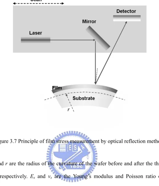
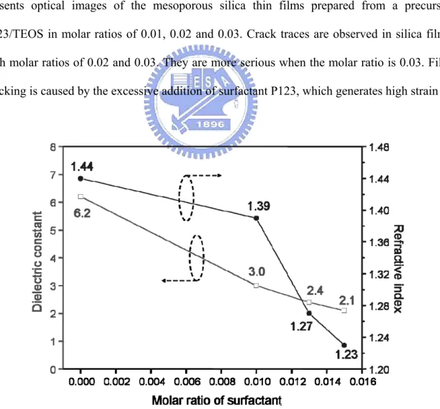
(14) Figure 3.6. Schematic representation of (a) a cross section of a surface through an indentation, and (b) the load-displacement relationships………………………44. Figure 3.7. Principle of film stress measurement by optical reflection method……............46. Figure 4.1. FTIR spectra of (a) the as-baked film, and the as-baked film followed by calcination at (b) 200oC for 90 min, (c) 300oC for 90 min, (d) 350oC for 30 min, and (e) 400oC for 30 min………………………………………….....................50. Figure 4.2. Dielectric constant and refractive index of the mesoporous silica thin films as a function of surfactant/TEOS molar ratio……………………………………….51. Figure 4.3. Surface morphologies of the mesoporous silica thin films prepared from a precursor P123/TEOS in molar ratios of (a) 0.01, (b) 0.02 and (c) 0.03.............52. Figure 4.4. FTIR spectra of mesoporous silica thin film; (a) as-calcined film, (b) as-calcined film after HMDS treatment for 30 min, (c) as-calcined TMCS (10% molar ratio) derivatized film, (d) TMCS derivatized film after HMDS treatment for 30 min……………………………………………………………………………...54. Figure 4.5. Trimethylsilylation of mesoporous silica thin films by HMDS. A HMDS molecule reacts with surface silanol group, to give a silylated pore surface and (CH 3 ) 3 SiNH 2 , which then reacts with a Si-OH group yielding NH 3 as byproduct……………………………………………………………….............55. Figure 4.6. Thermal desorption spectra of H2O (m/e = 18) for the as-calcined (dash line) and the HMDS treated (solid line) mesoporous silica thin films………...................56. Figure 4.7. High frequency (1 MHz) C-V characteristic and leakage current of mesoporous silica film after HMDS treatment…………........................................................57. Figure 4.8. Capacitance-voltage curve and leakage current for TMCS derivatized mesoporous silica film………………………………………………….............58. Figure 4.9. FTIR spectra of mesoporous silica thin film; (a) as-calcined film, (b) as-calcined. -xii-.
(15) film after H2 plasma treatment for 3 min, (c) H2 plasma treated film after HMDS treatment for 20 min, (d) H2 plasma treated film after HMDS treatment for 30 min……………………………………………………………………………60 Figure 4.10 Schematic representation of trimethylsilylated mesoporous silica thin films subjected to hydrogen plasma treatment………………………….....................60 Figure 4.11 FTIR spectra of HMDS treated mesoporous silica thin film after H2 plasma treatment for (a) 0 min, (b) 2 min, (c) 3 min, and (d) 10 min………………….61 Figure 5.1. Cross-sectional SEM image of as-calcined mesoporous silica thin film. The thickness is estimated to be about 300 nm……………………………………..64. Figure 5.2. AFM image of the as-calcined mesoporous silica thin film. The image size is 5 x 5 μm2…………………………………………………………………………...65. Figure 5.3. XRD spectra of the as-calcined mesoporous silica thin films; (a) without TMCS derivatization, (b) with 10% molar ratio TMCS, (c) with 15% TMCS, and (d) 25% TMCS. For clarity, the XRD spectrum of the mesporous film with 5% TMCS is not shown. The (100) diffraction peak of the silica film with 5% TMCS is situated at 2θ = 1.42, and has an intensity and a fwhm comparable to the mesoporous film with 10% TMCS…………………………………………66. Figure 5.4. SEM images of the as-calcined mesoporous silica thin films with 15% molar ratio TMCS derivatization. The magnification is (a) 500x and (b) 3000x…......67. Figure 5.5. Curve fitting for the absorption band of the Si-O-Si asymmetric stretching modes of as-calcined mesoporous silica film without TMCS modification, assuming a Gaussian shape for the resolved peaks. For comparison, the absorption band of the TMCS (5%) derivatized film is also shown in the figure (dashed line). A broader and symmetric absorption feature at the low wavenumber side can be clearly seen for the TMCS derivatized film. The. -xiii-.
(16) broader feature is ascribed to the presence of cyclosiloxane like rings as explained in the discussion……………………………………………………..69 Figure 5.6. Asymmetric stretching motion of the (a) TO3 and (b) TO4 modes of the intertetrahedral oxygen in the SiO2 network…………………….……………..69. Figure 5.7. FTIR spectra of mesoporous silica thin films in the range of the Si-O-Si asymmetric stretching modes; (a) the as-calcined film, (b) the as-calcined film after the HMDS treatment for 30 min, (c) the as-calcined film with 5% TMCS, (d) the as-calcined film with 10% TMCS. The small peak at 1258 cm-1 is due to the Si-CH3 stretching mode………………………………………………….71. Figure 5.8. Young’s modulus and hardness of the mesoporous silica thin films; (a) the as-calcined film, (b) the as-calcined film after the HMDS treatment for 30 min, (c) the as-calcined TMCS (5% molar ratio) derivatized film, (d) the TMCS (5% molar ratio) derivatized film after the HMDS treatment for 30 min, (e) the as-calcined TMCS (10% molar ratio) derivatized film, (f) the TMCS (10% molar ratio) derivatized film after the HMDS treatment for 30 min…………...72. Figure 6.1. Cross-sectional SEM image of the mesoporous SiO2/α-SiC:H/mesoporous SiO2 sandwich film structure…………………………………………………...........78. Figure 6.2. Film thickness of the mesoporous SiO2 thin film after various steps of the film preparation process. The film thickness was examined by cross-sectional SEM. Also shown in the figure is the film stress of the mesoporous film……………79. Figure 6.3. FTIR spectrum of the mesoporous silica thin film after the HMDS treatment for 30 minutes. The inset shows the absorption band around 1258 cm-1, which is due to the Si-(CH3)3 stretch vibration, for (a) the as-calcined film, and for the mesoporous silica after the HMDS treatment for (b) 30 min, (c) 60 min, (d) 90 min……………………………………………………………………………...80. -xiv-.
(17) Figure 6.4. Elastic modulus and hardness of the mesoporous silica thin films as a function of the HMDS exposure time……………………………………………………81. Figure 6.5. Film stress of the mesoporous SiO2 as a function of surfactant/TEOS molar ratio……………………………………………………………………………..82. Figure 6.6. Film stresses of three mesoporous SiO2/α-SiC:H film stacks at different preparation stages. The α-SiC:H capping layer was deposited at (a) 150oC, (b) 250oC, and (c) 350oC…………………………………………………………...83. Figure 6.7. Film stress and refractive index of the α-SiC:H film deposited on the Si wafer as a function of deposition temperature...…………………………………………84. Figure 6.8. Auger intensity ratios of carbon to oxygen and to silicon for mesoporous silica/α-SiC:H film stacks as a function of α-SiC:H deposition temperature….85. Figure 6.9. Stress as a function temperature during thermal cycling for mesoporous silica film on Si and Ge substrates; (a)the as-calcined film and (b) the methylsilylated film……………………………………………………......................................87. Figure 7.1. Thermal desorption spectra of CH4 (m/e = 16) for the as-calcined (dash line) and the HMDS treated (solid line) mesoporous silica thin films…………………...91. Figure 7.2. (a) FTIR spectra of (i) the as-calcined film, (ii) the HMDS treated film, and the HMDS treated film annealed at (iii) 300oC, (iv) 400oC, (v) 500oC, and (vi) 600oC. The enlarged absorption spectrum windows for the C-H stretching and the Si-O-Si asymmetric stretching modes are shown in (b) and (c), respectively……………………………………………………………………..92. Figure 7.3. AES depth profiles of the SiNx/Cu/Ta(N)/mesoporous SiO2/Si film stack after (a) 450oC annealed and (b) 600oC annealed…………………………………….....97. Figure 7.4. Cross-sectional TEM images of the metallized film stack after (a) 450oC annealed and (b) 600oC annealed………………………………………………99 -xv-.
(18) Figure 7.5. High resolusion TEM micrograph of the Ta 2 C nanocrystal at the Ta(N)/mesoporous silica interface of the sample annealed at 600oC for 30 minutes………………………………………………………………………..100. Figure 7.6. C-V traces of Cu-MIS capacitors stressed under various gate biases at 150oC for 15 min: (a) unannealed capacitor, and (b) capacitor annealed at 400oC……...102. -xvi-.
(19) List of Symbols. A: the contact area of an indenter C: the capacitance of material D: the line spacing of interconnect E: the elastic modulus of material Ei: the elastic modulus of the indenter Er: the reduced elastic modulus Es: the Young’s modulus of the bare substrate H: the hardness of material J: the leakage current density L: the length of the metal line M: the line thickness of interconnect Mf: the biaxial modulus of the film N: the number of molecules per m3 P: the line pitch of interconnect Pc: the power consumption Pm: the maximum load R: the resistance of material S: the stiffness of material Tg: the glass transition temperature V: the supply voltage Vf: the total volume of the film Vp: the volume of the pores W: the line width of interconnect -xvii-.
(20) f: the operational frequency fd: the fraction of gates that switch during a clock period g: the gradient of the stress as a function of temperature hc: the contact depth hm: the maximum depth of the elastic deformation under load hs: the displacement of the surface at the perimeter of the contact k: the relative dielectric constant of the insulator kbulk: the bulk dielectric constant keff: the effective dielectric constant n: the refractive index of the film r: the radius of the curvature of the wafer after the thin film was deposited r0: the radius of the curvature of the wafer before the thin film was deposited tf: the thickness of the film ts: the thickness of the substrate Π: the porosity of the film αe: the electronic polarization αf: the coefficients of thermal expansion of the film αi: the ionic polarization αo: the orientation polarization αs: the coefficients of thermal expansion of the substrate β: a geometrical constant of the indenter ε: a geometrical constant ε0: the permittivity of a vacuum εm: the permittivity of the solid matrix of the film εp: the permittivity of the internal pores of the film. -xviii-.
(21) εr: the relative permittivity of material θ: the X-ray diffraction angle ν: the Poisson’s ratio of material νi: the Poisson’s ratio of the indenter νs: the Poisson ratio of the bare substrate ρ: the metal resistivity σf: the film stress. -xix-.
(22) Chapter 1 Introduction. In recent decades, the field of solid-state electronics has a revolution and development continues at a remarkable rate. This development relies on the continuous miniaturization of devices in circuits [1], as forecasted by Intel’s cofounder Gordon Moore, allowing more components and more functions to be installed per unit area (Fig. 1.1). Now, the field of solid-state electronics is approaching the era of nanodevices, whose dimensions are under 100 nm. However, the over-shrinkage of integrated circuits has forced chipmakers to face difficult challenges, such as RC delay, crosstalk and power dissipation. The preferred strategy now is to introduce a copper conductor accompanied by an insulator with a low dielectric constant (low-k). This chapter offers an overview of the development of integrated circuit technology. The characteristics and requirements of low-k materials are also briefly considered here.. Figure 1.1 Complexity of MOSFET-based chips versus time [1]. -1-.
(23) 1.1 Multilayer Interconnect Technology for Scaling Developing ultralarge-scale integrated circuits (ULSI) depends on a scaling law, which states that the scaling of transistor dimensions increases chip performance. When the production dimensions of the transistor are reduced, the chip size can be reduced. Therefore, semiconductor makers can cut the unit manufacturing price by increasing the number of chips on each wafer. For instance, the 0.13 μm Pentium 4 processor, a product of Intel Corp., has 55 million transistors, and that becomes twice as many as a 90 nm microprocessor. Also, the scaling law establishes the possibility of increasing signal processing speed and power consumption as the transistor size is reduced. The industry remarkably doubles the device speed roughly every two years by reducing the gate size of the transistor by about 30% at every technology node. Faster, smaller, higher performance and lower cost ICs support the profitability of the industry today. However, the effective speed of a device is controlled not only by the intrinsic gate delay but also by the rate of signal propagation through the metal interconnect. Modern integrated circuit devices contain millions of transistors electrically connected by millions of wires fabricated on the wafer. These connect wires, or “interconnects”, transfer the signal between the transistors, and make the devices perform logic operations. Previously, the interconnect signal delay, characterized by the resistance-capacitance (RC) time constant, was negligible. As the device dimensions are reduced below 250 nm, the performance of ICs, historically limited by the characteristics of the transistors, has become limited by the interconnect RC delay, crosstalk and power consumption. Figure 1.2 presents a simple model of the cross-sectional view of multilevel interconnects, where P represents the line pitch, W the line width, D the line spacing and M the line thickness [2]. The thickness of the insulators above and below the interconnect is assumed to be equal. In a simple first-order model, the. -2-.
(24) Figure 1.2 Schematic diagram of a typical interconnect element [2].. RC time delay is given by Eq. (1.1).. (. ). RC = 2 ρkε 0 4 L2 / P 2 + L2 / M 2 ,. (1.1). where ρ is the metal resistivity, ε0 the vacuum permittivity, k the relative dielectric constant of the insulator and L the length of the line. The power consumption (Pc) of a circuit is given by, ⎛1⎞ Pc = ⎜ ⎟ f d CV 2 f , ⎝2⎠. (1.2). where C is the total on-capacitance, V the supply voltage, f the operational frequency and fd the fraction of gates that switch during a clock period. The drop in the size of features greatly increases the RC delay time, but introducing metallic interconnects with low electrical resistivity and intermetal dielectrics (IMD) with low permittivity can overcome the scaling hurdles. Additionally, reducing k, and therefore C, reduces the power dissipation (Pc) and makes the device more efficient, as indicated by Eq. (1.2). Until recently, all interconnects were fabricated using aluminum (ρ≒2.66 μΩ-cm) as the conductor and silicon dioxide (k=4.0) as the dielectric. Figure 1.3 reveals that the introduction of Cu (ρ≒1.67 μΩ-cm) and low-k dielectric (k=2.0) improves the RC delay at each IC technology node [3]. At the 0.25 μm technology node and beyond, using Cu and a low-k dielectric greatly reduces the delay time to about 65% lower than that obtained using Al and SiO2 at the sub-0.1 μm technology node.. -3-.
(25) Figure 1.3 Calculated gate and interconnect delay versus technology generation [3].. Figure 1.3 also reveals that switching SiO2 to low-k is more effective in improving the RC delay. The results are so important that they motivate not only researchers to invest their time in development but also the materials supplier to pay attention to the potential major economic benefits, which are as much as US $400 million per year in 2006 [4].. 1.2 Urgent Development of Intermetal Dielectric Materials with Ultralow Dielectric Constant The copper dual damascene process has been extensively adopted in the production line, but no consensus exists about the preferred IMD material for sub-65 nm technology nodes. In fact, the implementation of low-k IMD with a required k value was continuously revised from 1999 [5, 6]. The delay in the implementation of low-k IMD is attributable to the fact that many obstacles are difficult to overcome when low-k materials need to be successfully -4-.
(26) integrated in a dual damascene interconnect structure. According to the 2005 International Technology Roadmap for Semiconductors (ITRS), IMD materials with a bulk dielectric constant (kbulk)≤2.4 are expected to be used in 2007 [5]. In reaching such a low k value, many porous materials will be candidate ultralow-k dielectrics. Since air has a dielectric constant of about 1.0, introducing air into a dielectric can reduce the k value of the material as a whole. Therefore, the most logical strategy for reducing the k value of a dielectric is to reduce its mass density, or introduce pores into it [7-9]. However, high porosity raises many difficulties to the integration of porous ultralow-k dielectrics into the Cu damascene process. Tables 1.1 and 1.2 present the requirements and the best approximations to the defining characteristics of new IMD materials with k<3, respectively. More effort has to be made to improve the mechanical and thermal properties of porous materials because the porosity is responsible for weak mechanical strength and poor heat conduction. Also, dielectric stability throughout the processing of the device and during its actual use is extremely important. The pore structure of the porous dielectric strongly affects many process steps, including dry etching, wet cleaning and chemical mechanical polishing.. Table 1.1 Requirements for low-k IMD materials.. -5-.
(27) Table 1.2 Defining IMD characteristics.. -6-.
(28) Among various porous ultralow-k dielectrics, silica-based porous materials are most widely studied because they are chemically compatible with contemporary IC processes and k<2.5 can be easily achieved owing to the high porosity. However, as indicated above, the mechanical strength of porous silica dielectrics is far inferior to that of a dense silicon oxide IMD. Porous silica thin films with nanoscaled pores, including xerogel [10-12] and surfacant templated mesoporous silica [12-16], are typically fabricated by the sol-gel method. In particular, self-assembled molecularly templated mesoporous silica is regarded as a very promising ultralow-k dielectric because it has better mechanical and dielectric characteristics than xerogel because of the ordered pore structure and uniform pore size distribution (2-10 nm) [16-18]. Porous silica dielectrics prepared by the sol-gel approach are typically hydrophilic. Therefore, the uptake of moisture can severely reduce the dielectric stability of the porous materials. Trimethylsilylation method is commonly used to increase the hydrophobicity of porous silica thin film [14-22]. Methylsilylated porous silica thin films not only exhibit improved hydrophobicity, but also better mechanical and dielectric properties. Since they have much poorer mechanical properties than their condensed counterparts, more attention should be paid to mechanical problems associated with the integration of mesoporous silica dielectrics into the Cu interconnect structure. One of the mechanical challenges is to maintain satisfactory adhesion with adjacent layers and resist against delamination or cracking during various processes, including thermal and chemical mechanical polishing (CMP) processes. Mesoporous silica thin films prepared by the sol-gel method exhibit a large tensile stress after drying, because of film shrinkage; plasma-assisted α-SiC:H films typically have compressive stress, whose magnitude depends on the deposition temperature. When these two dielectric materials are combined in a dual damascene structure, concerns about the compatibility of their mechanical properties warrant a close examination of the film stress that develops in the. -7-.
(29) film stack that is composed of ultralow-k mesoporous silica and barrier/etch stop layers. This thesis studies the film stress of ultralow-k mesoporous silica thin film and the. α-SiC:H/mesoporous silica film stack. The effects of trimethylsilylation on the mechanical characteristics and the dielectric character of the mesoporous silica thin film were also studied. The insertion of trimethylsilyl groups into the pore surface introduces uncertainty in the thermal stability of the mesoporous thin film. A high thermal and chemical stability is certainly critical to the integration of the mesoporous silica dielectric into a copper interconnect. However, the organic trimethylsilyl group can withstand up to a certain temperature in thermal treatment, and may decompose during various high-temperature IC processes, causing severe damage to the interconnect structure. This work studies the thermal and dielectric stability of the HMDS-treated mesoporous silica thin film and its effect on the Cu-metallized mesoporous silica film stack.. 1.3 Organization of Thesis This work discusses the primary issues around porous low-k material integration. Self-assembled molecularly templated mesoporous silica thin films were prepared as low-k dielectrics. Some thin-film characterization approaches are adopted to analyze the electrical, mechanical and thermal properties of the mesoporous silica thin films and metal/dielectric film stacks. This dissertation is divided into seven chapters. The contents of each chapter are as follows. Chapter 1 introduces the motivation and organization of this dissertation. Chapter 2 reviews the literature. The factors that affect the dielectric constant of the materials are initially considered. Then, the general background of low-k materials, especially -8-.
(30) mesoporous silica thin films, and their application in backend Cu dual damascene process is presented. Chapter 3 introduces the experimental method and the analytic technology. Chapter 4 discusses the dielectric properties and hydrophobicity of self-assembled templated mesoporous silica thin films. Chapter 5 focuses on the microstructure and mechanical strength of mesoporous silica thin films. Chapter 6 discusses film stresses in the mesoporous silica dielectric and its stacks. The results of the thermal stress experiment are also discussed. The coefficient of thermal expansion of the mesoporous silica thin film is derived. Chapter 7 is concerned mainly with the thermal and electrical stability of mesoporous silica thin films. The thermal stability of metal/low-k film stacks was evaluated. Finally, Chapter 8 summarizes all experimental results. Some unfinished work is mentioned and new issues to be tackled in future studies suggested.. -9-.
(31) Chapter 2 Literature Review. Many materials, including ceramics and polymers, are electrical insulators and candidates for IMD applications. However, the most promising dielectric is one with material characteristics that can withstand the manufacturing process. This chapter reviews the dielectric properties, material characteristics of low-k dielectrics materials. Both organic and inorganic low-k dielectrics are considered.. 2.1 Electrical Performance of Low-k Dielectrics The basic electrical phenomenon of a dielectric material is polarization: an electric dipole moment can be induced by an electric field or can be permanent. A dielectric material can exhibit three forms of polarization in an applied electric field - electronic, ionic and orientation [23, 24]. Electronic polarization arises when the cloud of bound electrons is displaced from the nucleus of an atom, resulting in an electric dipole moment. Ionic polarization refers to the distortion of the position of the nuclei by the applied field, and, therefore, a change in the bond length. Some also refer to this as atomic polarization. If a molecule has a permanent electric dipole moment, which arises from the different electronegativity or other features of bonding, then polar molecules can exhibit orientation polarization in an applied field. These three polarization phenomena reveal at the specific frequency of an ac field and determine the polarizability of materials. For instance, orientation polarization involves the motion of complete molecules, so it does not resonate at a critical frequency, as do electronic and ionic polarization. Electronic polarization dominates at high. - 10 -.
(32) frequency (~1015 Hz), while the other two polarization are nuclear responses and are important at lower frequencies (<1013 Hz). Currently, typical device operating frequencies are 109 to 1010 Hz, and all three polarization contribute to the dielectric constant, as discussed below. (The maximum response frequency of orientation polarization is of the order of 109 Hz). Therefore, the polarization of IMD materials should be minimized to optimize performance. The relationship between the dielectric constant and the total polarization can be quantitatively described by the Clausius-Mossotti equation [24],. ε r −1 N = (α e + α i + α o ) , ε r + 2 3ε 0. (2.1). where εr the relative permittivity or dielectric constant of material, ε0 the permittivity of a vacuum and N the number of molecules per m3. The terms αe, αi and αo are the electronic, ionic and orientation polarizations in the molecule, respectively. According to the equation, the relative permittivity is smaller if materials contain fewer polar molecules. This fact offers an important clue to the fact that reducing the density N and the polarizabilities α can reduce the dielectric constant. Table 2.1 presents the polarizabilities of some typical chemical bonds [25]. C-F and C-C bonds have the lowest polarizability, indicating that the incorporation of fluorine atoms and reducing the number of double or triple bonds can effectively reduce the polarization of materials. The former is associated with high electronegativity, which causes tight binding of the electrons and increases free volume. The latter is associated with a drop in the mobility of the π electrons. Some fluorinated aliphatic hydrocarbon materials are designed using these rules for low-k applications. For example, polyimides, which are extensively adopted in microelectronics, have dielectric constant values in the range 2.9-3.4. Fluorine substitution can reduce the dielectric constant to a lower value of 2.6 [26].. - 11 -.
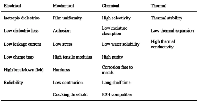
(33) Table 2.1 Electronic polarizability of some typical chemical bonds [25].. Although the contribution of polarization to the dielectric constant of materials is very important, the ways to reduce molecular polarizability are limited. Equation (2.1) also reveals that film density, like the chemical bonds, is important in reducing relative permittivity. Reducing the density is considered to be more effective because it can reduce k to close to unity. It can be performed using lighter atoms and/or by incorporating more free space around the atoms. Technologically, the best way to reduce film density is to introduce pores. Treating the porous film as two component materials, enables Eq. (2.1) to be rewritten as [27],. (ε p − 1) (ε − 1) ε r −1 , + (1 − Π ) ⋅ m = Π⋅ (ε p + 2) (ε m + 2) εr + 2 Π=. Vp Vf. ,. (2.2). (2.3). where εp and εm are the permittivity of the internal pores and the solid matrix of the film, respectively. The porosity of the film, Π, defined by Eq. (2.3), is the ratio that of the volume of the pores (Vp) to the total volume of the film (Vf). Equation (2.2) is also called the Bruggeman effective medium approximation and predicts the effect of porosity on the - 12 -.
(34) dielectric constant. Figure 2.1 presents the theoretical predication of the model for SiO2 (k=4) and a material with an original k value of 2.5. The curves reveal that the dielectric constant decreases as a function of porosity slightly faster than linearly. This fact is very useful to the material designer who wishes to estimate the minimum porosity required for a desired k value. For instance, to yield k=2.0, oxide materials require a porosity of about 50%. However, as presented in Fig. 2.1, a porosity of only ~30% is required for a k=2.5 low-k material, indicating that the lower k start value corresponds to a lower required porosity, potentially increasing the integration compatibility of the low-k materials. Additionally, the k values in Fig. 2.1 are ideal (for a dry film) and quite different from typical experimental values. In a real case, the reserve environment and the test methods affect the results. Most oxides contain many terminal OH groups and thus adsorb water. This trapped water (k≒78) or chemicals are likely to increase the dielectric constant and promote crack formation; a k value of below 2.0. Relative dielectric constant. is difficult to obtain even though the porosity is increased.. 4 Oxide k~4.0. 3 2. Low k~2.5 1 0. 0. 20. 40. 60. 80. 100. Porosity (%) Figure 2.1 Bruggeman’s effective medium approximation showing dielectric constant versus porosity for oxide and a low-k material.. - 13 -.
(35) 2.2 Potential Solutions for Creating Low-k Dielectrics Many low-k materials, including organic and inorganic dielectrics, have been proposed as replacements for the traditional CVD SiO2. The dielectric constant of CVD SiO2 films is 4.0±0.2, and dielectrics with a k value of below 4.0 are defined as low-k dielectric materials. SEMATECH has basically characterized several classes of candidate low-k materials. Table 2.2 presents the results. These candidate low-k materials are generally categorized as follows. 1. Oxides or organic polymers 2. Organic, inorganic or hybrid materials 3. CVD or spin-on methods 4. Fluorinated or nonfluorinated materials 5. Porous or nonporous materials This section introduces the potential low-k materials. The material characterization and integration issues of them are presented for comparison.. 2.2.1 Fluorosilicate Glass (FSG) Fluorine atoms were initially incorporated into SiO2 to reduce the k value relative to that of the traditional silicate glass, SiO2, in the development of low-k materials and fluorosilicate glass, FSG. The fabrication of FSG involves chemical vapor deposition, which process extends traditional SiO2 manufacture. Therefore, this material has attracted the attention of chipmakers. Figure 2.2 presents the chemical structure of FSG. Since fluorine is very electronegative, the incorporation of fluorine atoms reduces the polarization of SiO2, decreasing the dielectric constant, as described in section 2.1. Additionally, more terminal Si-F bonds result in a looser SiO2 structure and a drop in the density of the film. Therefore, the dielectric constant of SiO2 can be reduced; the drop depends on the concentration of. - 14 -.
(36) Table 2.2 Classification of low-k candidates.. fluorine. Experimentally, adding 10-15 at% F to SiO2 can reduce the k value by 20% to about 3.3. Although fluorosilicate glass can be fabricated by many thin film deposition approaches, including TEOS-CVD, ECR-CVD, AP-CVD and LP-CVD, the most general approach is high-density plasma CVD (HDP-CVD). SiH4 and fluorides (such as SiF4, C2F6, CF4 or TEFS) as the gas source support simultaneous deposition and etch back, resulting in good gapfilling capacity without any void even for a width of 0.25 μm [28]. FSG has now been introduced into 0.25 and 0.18 μm IC production lines because of its chemical compatibility with IC processes. However, the thermal stability of fluorine is lower, potentially making the. - 15 -.
(37) Figure 2.2 Chemical structures of FSG with (a) low fluorine concentration, (b) high fluorine concentration.. dielectric unstable. The thermal treatment temperature should be under 450oC, when FSG films are used for IMD. Additionally, although the incorporation of fluorine makes the geometry of the Si-O network less polarizable, the concentration should be less than 10 at% to ensure the stability of the film, because the drop in film density provides more free space for the adsorption of moisture. This limitation in the fluorine concentration or in dielectric constant, causes the FSG films to fail at the 0.13 μm IC technology node and below.. 2.2.2 Silsesquioxane (SSQ)-based Materials Silsesquioxane-based materials comprise the inorganic Si-O bonding unit and organic substituents of low molecular weight, or hydrogen. Empirically, they have the chemical formula (R-SiO1.5)n where the substituent R may be hydrogen, alkyl, alkenyl, alkoxy or aryl. Their name is derived from the sesqui-stoichiometry of oxygen atoms bound to a silicon atom, and they are therefore also called “T-resin” (tri-substituted). The most common structures are oligomers with a cage (T8 cube, eight silicon atoms on the vertices of the cube) or a ladder structure [29], as presented in Fig. 2.3.. - 16 -.
(38) Figure 2.3 Ladder (a) and cage (b-d) structures of Silsesquioxanes [29].. Organic substitution on Si causes the SSQ oligomer commonly to dissolve in an organic solvent as a precursor, before it is spin-coated on a substrate. These precursor solutions, developed by many famous suppliers of chemical materials, can yield SSQ low-k films with k<3.0, as indicated in Table 2.3. Following spin-on, the film has the characteristics of a liquid gel. It necessarily suffers baking and curing steps, which promote the formation of a. Table 2.3 Available SSQ-based low-k materials.. - 17 -.
(39) three-dimensional network siloxane (Si-O-Si) skeleton. During baking, the residual solvent is removed. Further curing results in polycondensation, which forms the mutually bonded silsesquioxane units [30]. Liu et al. [31], and Liou and Pretzer [32, 33] backed at 180-250oC for MSQ and 150-350oC for HSQ, following curing above 400oC; the as-cured films had dielectric constants of 2.9-3.2. Although the siloxane matrix is chemically similar to SiO2, more than 25% non-bridging Si-R bonds yield a lower density than that of SiO2. The Si-R bond has a relative lower polarizability than the Si-O bond in SiO2. The lower density and polarizability bonds of SSQ are attributed to the lower k values in the range 2.5-3.3. The three common silsesquioxane compounds are recognized by the substituents R: Hydrogen-silsesquioxane (HSQ, HSSQ), Methyl-silsesquioxane (MSQ, MSSQ), Phenyl-silsesquioxane (PSQ, PSSQ). The material properties of these three silicate based materials vary greatly as indicated in Table 2.4. HSQ (H-SiO1.5) and MSQ (CH3-SiO1.5) are two low-k SSQ materials used commonly in microelectronic applications. HSQ has a k value in the range 3.0-3.2 but it involves many problems of integration. For instance, Liou and Pretzer [33] found that a network structure formed upon thermal processing at over 400oC due to the disassociation of Si-H bonds, which increases the difficulty of integration. MSQ has a dielectric constant of. Table 2.4 Material properties for SSQ-based matrix resins.. - 18 -.
(40) 2.8, lower than that of HSQ, because the the Si-CH3 bonds are larger but less polarizable than the Si-H bonds. It is also more stable during the thermal process. The challenge raised by HSQ is degradation during O2 plasma resist stripping, such that an alternative stripping technique, such as H2 plasma treatment, is required [31]. Additional pores are introduced into the matrix resins of both HSQ and MSQ by adding surfactant or porogen, to greatly reduce the dielectric constants. Table 2.3 presents some of the results, and the section on porous materials will present details of the pore-forming methods.. 2.2.3 Low-k Polymers Since the 1980s, a large group of researchers have studied many newly synthesized or pre-existing polymers for their use as IMDs. For example, polyimide, a traditional material used in IC packaging, has a low k value from 2.3 to 2.9. Such polymers are varied but most are inappropriate for use in actual Cu metallization. Seven main considerations limit their applicability: 1. poor thermal stability (weight loss >1.0% at under 450oC) 2. anisotropic thermal, electrical and mechanical properties 3. softness 4. poor thermal conductivity 5. moisture uptake and outgassing 6. poor adherence to other contact layers, including the metal line and the diffusion barrier 7. incompatibility with traditional technological processes developed for SiO2-based dielectrics. Figure 2.4 presents the chemical structures of some common polymer low-k materials. - 19 -.
(41) Figure 2.4 Chemical structures of (a) polyarylethers; (b) FLARETM; (c) Teflon AF; (d) divinylsiloxane-benzocyclobutene (DVS-BCB); (e) SiLK.. Notably, these materials often have symmetric monomer structures, balancing the polarizability of the polymers. Additionally, organic low-k polymers are typically synthesized as non-polar or polar polymers. Non-polar polymers comprise primarily non-polar C-C bonds. Therefore, they have dielectric constants that are independent of frequency, such that their dielectric losses are low. Unlike non-polar polymers, polar polymers have an asymmetric charge distribution, which arises from differences among the electronegativities of atoms. They therefore have higher dielectric loss and a dielectric constant that depends on frequency and temperature. Saturated hydrocarbons have a lower polarizability and dielectric constant than unsaturated, conjugated and aromatic hydrocarbons (Table 2.1). However, they typically suffer from thermal degradation at temperatures of 300-400oC, or even much lower temperature. Only materials with aromatic, ladder, cross-linked structures can tolerate. - 20 -.
(42) temperatures of 450-500oC, which are required for IC interconnects. This situation represents a dilemma but the designer must find a compromise between the dielectric constant and the thermal stability when producing reliable polymer dielectric films. Empirically, most low-k polymer films with sufficient thermal stability have dielectric constants of 2.6-2.8. In the last five years, low-k polymers have remained attractive to some researchers because of their properties are variable [34, 35]. These variations in the properties of polymers involve the partial rearrangement of monomers [36, 37]. Two polymers, PVDF [poly(vinylidene fluoride)] and PTFE [poly(tetrafluoroethene) or Teflon], have very similar chemical structures, but widely different properties. As presented in Fig. 2.5, the difference between these polymers that the two hydrogen atoms in PVDF are replaced by two fluorine atoms in PTFE. This slight difference between bonding atoms makes PVDF soluble in a polar solvent and PTFE is insoluble in organic solvents. Additionally, replacing the hydrogen with larger side groups can generate asymmetry in the polymer chain, reducing the tendency of the chains to slide past each other and increasing the tendency to form bonds between the chains, improving rigidity and increasing the melting point. Another case of interest involves copolymer, which replaces the side of the polymer chain with two or more polymer branches. Such branched structures may reduce the packing density of linear polymer, affecting the mechanical properties and the thermally induced glass transition temperature, Tg. (More branching corresponds to lower crystallinity).. Figure 2.5 Chemical structure of PTFE and PVDF.. - 21 -.
(43) The glass transition temperature is some temperature, or narrow range of temperatures below which an amorphous polymer is in a glassy state, and above which it is rubbery. Polymer is glass or rubbery, depending on whether its application temperature is above or below its Tg (>450-500oC for low-k films). The degree of cross-linking, which affects the thermal [38] and mechanical [39] properties of low-k polymer materials, also affects their glass transition temperature. Polymer chains may chemically link to each other via the reactive groups, to form a 3D network, in a process called cross-linking, which typically occurs during curing, improving stiffness, and ensuring that the behavior prior to plastic deformation under a load is sustainable. Heavily cross-linked polymers, or thermosetting polymers, typically have a high Tg and better mechanical yield strength. They are generally brittle [40]. Epoxies, polyurethane, parylenes, polyimide siloxanes, polyimides and FPI (fluorinated polyimides), benzocyclobutene (BCB) [41], SiLKTM [42, 43], FLARETM [fluorinated poly(arylethers)] [44], PAE [poly(arylethers)], HOSPTM (hybrid organosiloxane) [44] and perfluorocyclobutane are such polymers and are preferred for use in IMD applications. Figure 2.4 presents the chemical structures of PAE, FLARETM, BCB and SiLKTM low-k materials. These organic polymers with a dielectric constant in the range 2.5-3.0 contain large amounts of benzene or fluorine, and, therefore, have low dielectric constants and good thermal stability. They share the problems of poor mechanical strength and poor adhesion. Therefore, a capping oxide layer and an adhesion promoter must be added to each for integration. Table 2.5 also presents some of the polymers adopted in IMD applications. Another focus of low-k polymer candidates is SiLKTM resin. SiLKTM is a spin-on hydrocarbon dielectric [5, 6, 42, 43, 45], which was developed by the Dow Chemical company. In 2000, IBM Microelectronics first used this dielectric material was first used in 0.13 μm BEOL. Figure 2.6 presents a four-level metal SRAM structure with a three-level. - 22 -.
(44) Table 2.5 Some of the polymers for low-k application.. SiLKTM dielectric [5]. Water is typically generated during curing because of dehydration in the condensation reaction in the synthesis of polymer from monomers. The SiLKTM resin is an extremely dense aromatic hydrocarbon (Fig. 2.4e) and releases no moisture as a byproduct during curing. Table 2.6 summarizes the main properties of SiLKTM dielectric. As indicated in the table, SiLKTM has a k value of 2.6 and Tg>490oC, resulting in thermal stability over 425oC. Its intrinsic properties are so intriguing that UMC actively developed it as IMD [46]. However, UMC announced that it was ending its development of SiLKTM and in Feb. 2002, when it began to use FSG and CoralTM (carbon-doped oxide). After two years, IBM also considered abandoning SiLKTM because its CTE (which is a function of temperature) is too high at temperatures of over 150oC [47]. Although other refinements were subsequently announced, they did not satisfy the chipmakers. Nowadays, some Japanese companies like SONY and Fujitsu use a hybrid scheme as an IMD structure. - 23 -.
(45) Figure 2.6 SEM cross-sectional image of Cu-SiLKTM interconnect structure [5].. Table 2.6 Intrinsic properties of SiLKTM low-k dielectric.. - 24 -.
(46) 2.2.4 Amorphous Carbon The use of fluorinated amorphous carbon (a-C:F) thin films as IMDs with low dielectric constants was recently reported [39, 48-59]. Sometimes, such materials are given such names as diamond-like carbon (DLC), hydrogenated DLC, fluorine-containing DLC (FDLC) [51, 52], plasma-polymerized fluorocarbon (PPFC) [53], fluorinated amorphous-carbon (a-C:F:H) [39] and amorphous carbon fluoride (a-CF) [54]. All these films have a wide range of k values from 2.0 to 3.6 and are typically formed by plasma-enhanced CVD (PECVD) using a discharge with fluoro-carbon gases (such as CF4, C2F6, C4F8 + CH4 or hydrogen mixtures). The film comprises amorphous C-C cross-linked bonds (mixing of sp3 and sp2 bonding) and C-F bonds with a PTFE-like structure. Controlling the F/C ratio of an a-C:F film is important because it is the factor that most strongly affects the dielectric constant and the thermal stability. C-F bonds with a weak tendency to polarize in external electrical fields can reduce the dielectric constant of the a-C:F thin film, but excess C-F bonds suppress the formation of C-C cross-links, which would otherwise maintain the film’s thermal stability. Therefore, the properties of the a-C:F thin films can be adjusted easily by changing the plasma process conditions.. 2.2.5 Carbon-doped Silica Alkyl groups, like fluorine, can be incorporated into silicon dioxide to reduce its k value. It is called carbon-doped oxide (CDO) [also known as organosilicate glass (OSG), or silicon oxicarbide (SiOCH)]. Carbon-doped oxide films can be deposited at ≥400oC by PECVD, typically using O2 and such precursors as methylsilane (1MS, H3SiCH3), dimethylsilane [2MS, H2Si(CH3)2], trimethylsilane [3MS, HSi(CH3)3], tetramethylsilane [4MS, Si(CH3)4] [60-62], and other methyl-based sources, including tetramethylcyclotetrasiloxane (TMCTS) [63, 64], octamethylcyclotetrasiloxane (OMCTS) [65] and dimethyldimethoxysilane (DMDMOS) [66]. - 25 -.
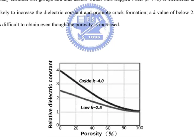
(47) Of these, 3MS is the most widely accepted precursor for depositing CDO films because it is safe and the industry is familiar with it. CDO film has a dielectric constant of between 2.2 and 3.0, determined by the amount of methyl dopants. These dopants terminate some Si-O bond links in the oxide matrix, and reduce the electronic polarizability of the film. However, adding more carbon may create more problems such as cracking, softness and lack of adhesion. Precursors with more methyl groups can generally incorporate more carbon into the film, replacing 10-25% of the Si atoms [66-67]. The incorporated methyl groups also influence the physical, chemical and thermal properties of the CDO films. Table 2.7 presents some characteristics of the CDO films. CDO films have good thermal conductivity (~0.9 W/mC for PE-SiO2) and a coefficient of thermal expansion (CTE) that is close to those of Cu (~17.7 ppm/oC) and TaN (~6 ppm/oC). Therefore, the CDO thin films resist cracking and peering when integrated into a Cu interconnect. Well-known commercial CDO materials are CoralTM from Novellus Systems Inc. [68] and Black DiamondTM from Applied Materials Inc. [69]. The k value of Black DiamondTM II is less than 2.7 and is acceptable for 90 nm chips. Recently, TSMC decided to use a low-k Black Diamond system as its 90 nm process IMD [70, 71]. CDO dielectrics now seem to dominate the market of 90 nm IC products.. Table 2.7 Film properties of carbon-doped oxide and PECVD oxide.. - 26 -.
數據
![Figure 1.1 Complexity of MOSFET-based chips versus time [1].](https://thumb-ap.123doks.com/thumbv2/9libinfo/8099927.165116/22.892.281.662.736.1090/figure-complexity-mosfet-based-chips-versus-time.webp)
![Figure 1.3 Calculated gate and interconnect delay versus technology generation [3].](https://thumb-ap.123doks.com/thumbv2/9libinfo/8099927.165116/25.892.147.788.108.493/figure-calculated-gate-interconnect-delay-versus-technology-generation.webp)
+7
![Figure 2.6 SEM cross-sectional image of Cu-SiLK TM interconnect structure [5].](https://thumb-ap.123doks.com/thumbv2/9libinfo/8099927.165116/45.892.191.747.105.415/figure-sem-cross-sectional-image-silk-interconnect-structure.webp)
![Figure 3.2 Acid-catalyzed hydrolysis proceeds by bimolecular nucleophilic displacement reactions [81]](https://thumb-ap.123doks.com/thumbv2/9libinfo/8099927.165116/59.892.175.760.111.267/figure-catalyzed-hydrolysis-proceeds-bimolecular-nucleophilic-displacement-reactions.webp)
Outline
Organization of Thesis
Microstructure, Surface Morphology and Optical Properties
Summary
Microstucture of Mesoporous Silica Thin Films
Effect of Methylsilylation on the Mechanical Properties
Film Stress Relaxation
Thermomechanical Characteristics
Thermal and Chemical Stability of the Cu/Ta(N)-metallized Mesoporous Silica Film
Suggestions for Future Work
相關文件
volume suppressed mass: (TeV) 2 /M P ∼ 10 −4 eV → mm range can be experimentally tested for any number of extra dimensions - Light U(1) gauge bosons: no derivative couplings. =>
For pedagogical purposes, let us start consideration from a simple one-dimensional (1D) system, where electrons are confined to a chain parallel to the x axis. As it is well known
The observed small neutrino masses strongly suggest the presence of super heavy Majorana neutrinos N. Out-of-thermal equilibrium processes may be easily realized around the
Define instead the imaginary.. potential, magnetic field, lattice…) Dirac-BdG Hamiltonian:. with small, and matrix
incapable to extract any quantities from QCD, nor to tackle the most interesting physics, namely, the spontaneously chiral symmetry breaking and the color confinement..
(1) Determine a hypersurface on which matching condition is given.. (2) Determine a
• Formation of massive primordial stars as origin of objects in the early universe. • Supernova explosions might be visible to the most
The difference resulted from the co- existence of two kinds of words in Buddhist scriptures a foreign words in which di- syllabic words are dominant, and most of them are the
