deposition
D.-S. Lin, T. Miller, and T.-C. Chiang
Citation: Journal of Vacuum Science & Technology A 15, 919 (1997); doi: 10.1116/1.580623 View online: http://dx.doi.org/10.1116/1.580623
View Table of Contents: http://scitation.aip.org/content/avs/journal/jvsta/15/3?ver=pdfcov
Published by the AVS: Science & Technology of Materials, Interfaces, and Processing
Articles you may be interested in
Strain induced intermixing of Ge atoms in Si epitaxial layer on Ge(111)
J. Appl. Phys. 113, 073511 (2013); 10.1063/1.4792503
Ge film growth in the presence of Sb by metal organic chemical vapor deposition
J. Appl. Phys. 102, 083531 (2007); 10.1063/1.2795673
Ultrathin low temperature SiGe buffer for the growth of high quality Ge epilayer on Si(100) by ultrahigh vacuum chemical vapor deposition
Appl. Phys. Lett. 90, 092108 (2007); 10.1063/1.2709993
Low-temperature, chemically driven atomic-layer epitaxy: In situ monitored growth of CdS/ZnSe(100)
Appl. Phys. Lett. 71, 3799 (1997); 10.1063/1.120509
Effect of atomic hydrogen on the growth of Ge/Si(100)
chemical vapor deposition
D.-S. LinInstitute of Physics, National Chiao-Tung University, Hsinchu, Taiwan, Republic of China T. Miller and T.-C. Chianga)
Department of Physics and Materials Research Laboratory, University of Illinois, Urbana, Illinois 61801 ~Received 25 September 1996; accepted 17 February 1997!
Si and Ge films can be prepared under ultrahigh vacuum conditions by chemical vapor deposition using disilane and digermane as source gases. These gases offer a high sticking probability, and are suitable for atomic layer epitaxy. Using synchrotron radiation photoemission spectroscopy and scanning tunneling microscopy, we have examined the surface processes associated with the heteroepitaxial growth of Ge/Si. The measured surface-induced shifts and chemical shifts of the Si 2p and Ge 3d core levels allow us to identify the surface species and to determine the surface chemical composition, and this information is correlated with the atomic features observed by scanning tunneling microscopy. Issues related to precursor dissociation, attachment to dangling bonds, diffusion, surface segregation, growth morphology, and pyrolytic reaction pathways will be discussed. © 1997 American Vacuum Society.@S0734-2101~97!07003-6#
I. INTRODUCTION
Preparation of Si-Ge interfaces by vapor deposition under ultrahigh vacuum~UHV! conditions is a subject of consider-able interest to fundamental thin film science. These inter-faces represent a simple ‘‘prototypical’’ system involving two elemental materials with similar physical and chemical properties, and yet a variety of interesting effects are ex-pected because~1! the large lattice mismatch between Si and Ge causes strain in the overlayer, which is likely to affect the film morphology; and~2! Ge has a lower surface energy than Si, and therefore there is a tendency for Ge to segregate to the surface. Films of Si and Ge and their alloys are useful for a variety of electronic and optoelectronic device applica-tions, and a detailed understanding of the atomistics of the growth is important for the engineering of interface structure and properties.
The present article discusses the atomic processes associ-ated with UHV chemical vapor deposition~CVD! growth of Si and Ge films. The gases employed in this study are Si2H6 ~disilane! and Ge2H6 ~digermane!.1–16 These gases
have low decomposition activation energies, and a high growth rate can be achieved at fairly low growth tempera-tures. The techniques employed in this study include photo-emission spectroscopy and scanning tunneling microscopy ~STM!. Photoemission spectra of the Si and Ge core levels show surface-induced shifts and chemical shifts caused by bonding to hydrogen. A measurement of the relative intensi-ties of the various surface components provides a chemical analysis of the surface. This information allows one to ad-dress questions such as which atoms ~Ge or Si! are on the surface, and whether or not these surface atoms are bonded to hydrogen. STM, on the other hand, allows direct viewing of the surface atomic structure and morphology, and thus
provides complementary information. Previous studies em-ploying temperature programmed desorption, infrared spec-troscopy, electron energy loss, and other techniques have yielded additional information regarding the desorption tem-peratures and the chemical species on the surface.1–13All of the available information together yields a detailed atomistic description of the pyrolytic reactions and growth behaviors. Our experimental approach is to expose the surface to the CVD gas with the substrate typically held at room tempera-ture. The sample is then annealed for a fixed period of time ~60 s!, and allowed to cool down before examination. This cycle is repeated for increasing annealing temperatures, and the results reveal the chemical reactions and atomic pro-cesses occurring in different temperature ranges. For Ge deposition on Si~100! and Si deposition on Ge~100!, the ini-tial sticking coefficient is high, and the coverage quickly saturates at about one-half of a monolayer~ML!. After a high temperature anneal to drive off all of the surface hydrogen, the net deposition is ;1/2 ML. This quantized deposition can be repeated to build up a film with a precisely control-lable thickness, and this process is known as atomic layer epitaxy.
The desorption temperatures of hydrogen from Si and Ge surfaces are significantly different because of a difference in bond energy. This difference may cause a transfer of hydro-gen between Si and Ge upon annealing if both kinds of at-oms are present on the surface. The interplay of surface en-ergy, strain enen-ergy, and bond energy results in a variety of interesting effects that can be observed and studied in detail by photoemission and STM. It is not surprising that there are significant differences in the growth behaviors between Si on Ge and Ge on Si. Significant differences are also observed between the~100! and ~111! faces,16although our discussion will be mainly for the~100! results due to space limitations. a!Electronic mail: [email protected]
II. EXPERIMENTAL TECHNIQUES
Our STM measurements involve two instruments. One is homemade, and the other is an Omicron variable-tempe-rature STM. Large-area scans that will be discussed below were generally low-pass filtered to remove a background in order to enhance the local features. These pictures resemble landscapes with oblique light illumination from the left. Atomic steps appear either bright or dark depending on the step direction. Atomic-resolution pictures over smaller areas are unaffected by this filtering, and bright parts simply rep-resent protrusions. The photoemission measurements were carried out at the Synchrotron Radiation Center in Stough-ton, Wisconsin, and at the Synchrotron Radiation Research Center in Hsinchu, Taiwan. The same sample preparation procedure was employed in all of these separate measure-ments. Commercial Si and Ge wafers were used. The Si samples were cleaned by flash heating to about 1400 K, whereas the Ge samples were cleaned by repeated cycles of sputtering by Ar ions followed by annealing. After cleaning these surfaces exhibited sharp electron diffraction patterns. Digermane, diluted to 20% in He, and pure disilane were used for CVD growth. The ion gauge readings were cor-rected for the sensitivity to these gases. Heating of the sample was done by passing a current through the sample itself, and the temperature of the sample as a function of heating power was calibrated by attaching a small thermo-couple to the center of the back face of an identical test sample.
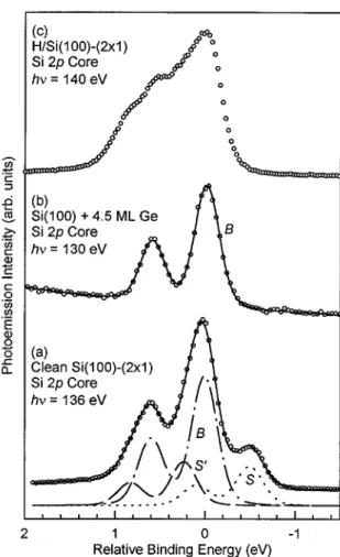
Figure 1~a! shows a typical Si 2p core level spectrum taken from a clean Si~100!-~231! surface. The line shape can be divided into three major components B~‘‘bulk’’!, S
8
~sur-face component 1!, and S ~surface component 2! as shown in Fig. 1~a!, where each component consists of a pair of spin-orbit-split peaks. The peak on the lower binding energy side in Fig. 1~a! is the 2p3/2 peak of the S component. It is well separated from the rest of the line shape, and its intensity can be deduced by fitting. This component is associated with the dimer atoms on the ~231! reconstructed surface, as was demonstrated in previous studies.17,20 The intensity of the unresolved S8
component cannot be easily deduced, and will not be used in this study.If the Si~100! surface becomes partially covered by Ge or H, the S component will diminish, and its intensity is a quan-titative measure of the surface area that remains clean. Shown in Fig. 1~b! is a spectrum of Si~100! covered by 4.5 ML Ge prepared by molecular beam epitaxy ~MBE!. Only the B component remains in the spectrum. This is because the bonding between Si and Ge is very similar to that be-tween Si and Si, and as a result, all Si atoms under such a thick layer of Ge are in a bulklike bonding environment. If the Si~100! surface is terminated by hydrogen, the core level spectrum will show hydrogen-induced chemical shifts to higher binding energy, as illustrated in Fig. 1~c!.15 The S component characteristic of the clean surface is not present. If the hydrogen is then driven off the surface by thermal annealing, the hydrogen-induced component will diminish, and the S component will reappear. A measurement of the
core level line shape thus provides a chemical analysis of the surface.
The Ge 3d core level spectrum taken from clean Ge ~100!-~231! shows a line shape very similar to Si~100!. There are again three major components, B, S
8
, and S, where the S component, shifted to lower binding energies, can be associ-ated with the dimers on the surface. This surface also shows a hydrogen-induced chemical shift. In our experiments, both the Si and Ge core level line shapes are measured.STM and electron diffraction reveal the surface symme-try. An observed ~231! reconstruction implies the presence of either Si or Ge dimer bonds on the surface, even though the dimer dangling bond could be terminated by either a H or a SiH3 ~GeH3) group. A surface terminated by SiH2
~GeH2) exhibits a local~131! structure.
III. RESULTS AND DISCUSSION
A. Adsorption and pyrolytic reactions for Si on Ge(100)
The results from all available experimental studies can be summarized by the following pyrolytic reactions for disilane adsorbed on Ge~100! for increasing substrate temperatures:
FIG. 1. Photoemission spectra for the Si 2p core level taken from~a! clean Si~100!-~231!, ~b! Si~100! covered by 4.5 ML of Ge prepared by MBE, and
~c! a monohydride-terminated Si~100! surface. The circles are data points,
and the solid curves are fits to the data. The fits involve three components (B, S8, and S) for~a!, and one component (B) for ~b!.
Si2H6~g!→2SiH3~s! ~RT!, ~1!
SiH3~s!1Ge~s!→SiH2~s!1GeH~s! ~RT–530 K!, ~2!
GeH~s!→Ge~s!1 1/2H2~g! ~530– 620 K!, ~3!
SiH2~s!1SiH2~s!→Si2H2~s! ~monohydride dimer!
1H2~g! ~530– 570 K!, ~4!
and
Si2H2~s!→2Si~b!1H2~g! ~630– 690 K!. ~5!
In these equations, (s), (b), and (g) refer to a surface spe-cies, an atom in the substrate below the surface, and a gas molecule, respectively. The approximate temperature range for each reaction is indicated, and RT refers to room tem-perature.
We will now examine the experimental evidence. Figure 2 shows Si 2p and Ge 3d core level spectra for various annealing temperatures starting from a Ge~100!-~231! sur-face saturated by disilane exposure at RT. The evolution of the main features as a function of annealing temperature is summarized in Fig. 3. Figure 3~a! is a plot of the intensity ratio between the S and B components of the Ge 3d core level, which is an indication of the surface area that is clean Ge~100!-~231!. Figure 3~b! is a plot of the intensity of the Si 2p core, where the significant drop in intensity indicates Si indiffusion. Figure 3~c! shows the binding energy shift of the Si 2p core level, which reflects chemical shifts as well as band bending shifts caused by a change in surface chemical composition. Four characteristic temperatures T1 – 45530,
570, 630, and 690 K and two transitions A ~between T1 and
T2) and B ~between T3 and T4) are indicated in the Fig. 3. Figure 4 shows a 2103250 Å2STM picture for 0.02
lang-muir ~L! exposure at RT. Randomly distributed adsorption sites are observed. Several possible bonding configurations for the molecular fragments are shown in Fig. 5. Configura-tion A corresponds to two SiH3bonded on the same side of
two neighboring dimers, resulting in an elongated bright pro-trusion located on one side of the two affected dimers. This is the dominant configuration found in our STM pictures. Configuration B involves the same two fragments bonded on the two dangling bonds of a single dimer. A very small frac-tion of the adsorpfrac-tion sites is characterized by configurafrac-tion C shown in Fig. 5. Again, two neighboring dimers are in-volved, and the images show a bright protrusion centered about the dimer row. This can be identified as two SiH2with
a local~131! structure; these SiH2fragments are formed as a
result of the decomposition of SiH3as indicated by Eq.~2!.
Configuration D in Fig. 5 corresponds to a monohydride dimer. This configuration is observed only after the sample has been annealed to higher temperatures. Note that the monohydride dimer has a local~231! structure similar to the dimer on the clean surface.
For all of these RT adsorption configurations ~A, B, and C!, the two fragments of dissociative chemisorption occupy
FIG. 2. Photoemission spectra for~a! Si 2p and ~b! Ge 3d core levels for various annealing temperatures as indicated. The sample is Ge~100! initially saturated by a 10 L disilane exposure at RT.
FIG. 3.~a! Intensity ratio of the S and B components of Ge 3d, ~b! integrated intensity of Si 2p, and~c! binding-energy shift of the Si 2p as a function of annealing temperature. The sample is Ge~100! initially saturated by a 10 L disilane exposure at RT. Two temperature ranges, A and B, and four tem-peratures, T12T4, associated with the reactions are indicated.
neighboring dangling bond sites, and this has an important implication. The initial sticking coefficient for disilane on Ge~100!-~231! is ;0.5 from our STM measurements. For the same experiment on the Ge~111!-c~238! surface, the sticking coefficient is reduced by three orders of mag-nitude.16This drastic difference can be related to the fact that two nearby Ge dangling bonds are needed for the
dissocia-tive chemisorption, and the distance between the two dan-gling bonds must match the Si-Si distance in Si2H6to
facili-tate the dissociation. This condition is well satisfied for the Ge~100! surface, but not for the Ge~111!-c~238! surface, for which neighboring dangling bonds on the surface are sepa-rated by much larger distances due to the c~238! recon-struction.16
As the exposure increases, more dissociative chemisorp-tion fragments are observed, and the surface becomes satu-rated for exposures greater than a few langmuirs. Because the pairs of dangling bonds involved in different adsorption events are not necessarily phase correlated, the resulting saturated surface appears disordered as seen by STM. Re-flection high-energy electron diffraction from the same sur-face, however, shows a~231! pattern, indicating that many of the dimer bonds underneath the disordered adlayer remain intact~care was taken to avoid surface modification by elec-tron beam irradiation!. This is consistent with the STM re-sults mentioned above that most fragments after a low expo-sure are SiH3.
As the annealing temperature increases, these SiH3
frag-ments dissociate into SiH2 according to Eq.~2!. This covers
a wide temperature range as indicated by Fig. 3~b!, which shows a continuous change of the Si 2p binding energy. The adlayer remains disordered. Transition A between T1 and
T2 is characterized by desorption of H from SiH2,
long-range diffusion of surface fragments to form monohydride islands, and desorption of H from GeH. After a 620 K an-neal, these processes are complete, and the surface is left with about 1/2 ML of silicon monohydride islands on an otherwise clean Ge~100!-~231! surface, as seen in Fig. 6~a!, which is a 5003500 Å2 STM picture. We know from the
~231! dimer reconstruction that these islands are in the form of silicon monohydride. We also know that the part of the surface not covered by these islands is clean Ge~100!-~231! because the intensity of the S component of the Ge core level has recovered to about one-half of the value for the clean surface, as seen in Fig. 3~a!.
Further annealing leads to transition B indicated in Fig. 3. The SiH islands lose H based on desorption measurements, and as soon as the H leaves, the Si left behind diffuses into a subsurface site because of the lower surface free energy of Ge relative to Si. This indiffusion is evidenced by the large drop in intensity of the Si 2p core level seen in Fig. 3~b!, which is accompanied by a large shift in binding energy seen in Fig. 3~c!. Simultaneously, the intensity of the S compo-nent of the Ge core level recovers to the clean surface value, as seen in Fig. 3~a!. Thus, the final configuration after tran-sition B is one in which all of the hydrogen is desorbed, the top layer is Ge, and the 1/2 ML of Si derived from the adsorbed Si2H6is in the subsurface region. Figure 6~b! is an
STM picture showing the~231! reconstruction of the top Ge layer.
It is interesting to note that Si indiffusion is correlated with the desorption of H from SiH. This is contrasted by the observed Si indiffusion at much lower temperatures during MBE growth of Si on Ge.21 Apparently, the presence of H
FIG. 4. A STM image of Ge~100!-~231! dosed by 0.02 L of disilane at RT. The area is 2103250 Å2.
FIG. 5. Schematic diagrams for various bonding configurations of disilane
fragments on Ge~100!-~231!.
bonded to Si in the CVD case hinders the indiffusion of Si. Another interesting effect is that the H desorption tempera-ture from the SiH islands on Ge~100! observed in this ex-periment is significantly lower than the desorption tempera-ture of H from the Si surface. This may be explained by a concerted motion involving Si, Ge, and H, or a mechanism involving the diffusion of H from the SiH islands onto a nearby exposed Ge surface where the H atoms can be readily desorbed because of the lower desorption temperature of H from GeH.
Some recent results have suggested that a mixed Si–Ge dimer layer consisting of Si atoms in the down dimer posi-tion and Ge atoms in the up dimer posiposi-tion might be ener-getically or kinetically more favorable under certain growth conditions in the preparation of Si–Ge interfaces.20,22 Our results show clearly that this is not the case for the system under study. If the Si atoms merely move into the down dimer positions, there would be little reduction in the Si core
level intensity, in disagreement with the data in Fig. 3~b!. Even though the measured core level intensity can be some-what affected by diffraction effects,23the intensity reduction is so large that these Si atoms cannot all reside in the layer just below the dimer layer. Some of the Si atoms must have moved into deeper layers. This is consistent with recent transmission electron microscopy~TEM! results which show that Si growth on Ge by MBE at similar temperatures results in an intermixed interface.24
Further annealing to even higher temperatures results in a further and gradual reduction of the Si core level intensity, indicating that the Si atoms are moving farther below the surface. Figures 7~a! and 7~b! show the surface morphology after a 720 and 820 K anneal, respectively, over a 4000 34000 Å2 area. The islands seen in Fig. 7~a! are mostly
absorbed by the steps with increasing annealing tempera-tures, but it is difficult to eliminate all islands. Figure 7~b! shows some remaining islands that should have been ab-sorbed by the step edges based on diffusion length consider-ations. This seems strange, but it can be explained by surface strain caused by the lattice mismatch between Si and Ge. Figures 7~c! and 7~d! show the surface morphology after 5 and 10 cycles of atomic layer epitaxy, where each cycle in-volves saturating the surface with disilane at room tempera-ture followed by annealing to 820 K. The effect of strain becomes clear now; the surface becomes covered by multilayer islands and holes to minimize the buildup of long-range strain. The lateral length scale becomes smaller as more growth cycles are performed. Detailed STM images show that the surface remains ~231! everywhere including the top of the islands and the bottom of the holes.
FIG. 6. 5003500 Å2STM images for Ge~100!-~231!, saturated with a 5 L disilane dose at RT, and then annealed to~a! 620 and ~b! 720 K.
FIG. 7. 400034000 Å2STM images of Ge~100!-~231!, saturated with a 5 L
disilane dose at RT, and then annealed to~a! 720 and ~b! 820 K. ~c!,~d! The same scale images of Ge~100! after ~c! 5 and ~d! 10 cycles of Si growth. Each cycle involves an exposure of 5 L disilane at 340 K followed by annealing at 820 K.
B. Adsorption and pyrolytic reactions for Ge on Si(100)
The initial sticking coefficient of digermane on Si~100! is again about 0.5, and the surface becomes saturated after an exposure of a few langmuirs. It might be expected that the annealing behavior of the digermane-saturated Si~100! sur-face should be generally similar to the case of Si on Ge~100!, and it is indeed the case based on our experiment. One im-portant difference is that the Ge remains on the surface after a high temperature anneal to desorb all H. In other words, the indiffusion of Si observed in the previous case has no coun-terpart for Ge growth on Si~100!. Figure 8 shows the Si and Ge core level line shapes as a function of annealing tempera-ture for a Si~100! surface initially saturated by digermane exposure. The Ge 3d line shape for the initial surface is broad because the Ge is in the form of a mixture of various hydrides. After annealing to 590 K, the line shape sharpens into that of GeH. The H is desorbed at even higher annealing temperatures, and the final Ge line shape consists of one major component, the S component, corresponding to Ge in the top dimer layer. The Si line shape in Fig. 8 shows that the
S component is eliminated by the adsorption, and partially
recovers for annealing temperatures higher than 770 K due to the desorption of H.
A very interesting coverage-dependent effect is observed. Figure 9 shows a comparison between two different initial digermane exposures, 0.2 and 1 L. The Ge core level spectra
in Fig. 9~c! indicate that the conversion of Ge hydrides into surface Ge becomes complete at 590 K for an initial expo-sure of 0.2 L. Figure 9~d! shows that the same conversion does not become complete until 650 K for an initial exposure of 1 L. The results in Fig. 8 further show that this conversion does not become complete until an even higher temperature of 770 K for a fully saturated surface. The explanation for this variation in temperature as a function of initial coverage is that the decomposition of GeH proceeds via two pathways: ~1! H2 desorbs directly from a monohydride dimer Ge2H2,
and ~2! a lower-temperature process in which the H atoms are transferred from GeH to nearby Si surface atoms to form SiH. The latter process is possible because the Si–H bond is stronger than the Ge–H bond as already noted above, but will require nearby Si dangling bonds, which are more abun-dant at lower digermane exposures. For higher initial diger-mane exposures, process~2! becomes suppressed due to the lack of available Si dangling bonds, leading to a higher tem-perature for the conversion of GeH into surface Ge. Figures 9~a! and 9~b! show the corresponding Si core level spectra. When H is transferred from GeH to Si during the annealing, one would expect the intensity of the S component of the Si core level to drop, and this is indeed observed. In Figs. 9~a! and 9~b!, the S intensity of Si decreases initially due to this effect, and increases at higher annealing temperatures when H is desorbed from Si.
STM observations show that the room-temperature
satu-FIG. 8. Photoemission spectra for Si 2p and Ge 3d core levels for various annealing temperatures as indicated. The sample is Si~100! initially satu-rated by a 15 L digermane exposure at 325 K.
FIG. 9.~a!,~b! Photoemission spectra of Si 2p at various annealing tempera-tures for an initial digermane exposure of 0.2 and 1.0 L, respectively.~c!,~d! The corresponding Ge 3d core level spectra.
rated surface is disordered as in the previous case. Figure 10~a! is a picture taken after annealing to 810 K. Here, one sees~231! islands covering roughly one-half of the surface. At this annealing temperature, there is very little H left on the surface. Annealing to an even higher temperature of 900 K causes the islands to coarsen and attach to step edges. This is illustrated in Fig. 10~b!. Dimer rows interrupted by miss-ing dimer defects are observed, and these defects tend to form rows perpendicular to the dimer rows. This is caused by strain, and the results are very similar to the (23n) recon-structions reported by other groups for the MBE growth of Ge on Si.22,25 This is not surprising, since at temperature high enough for complete H desorption, the growth should be similar for CVD and MBE. In contrast to the case of Si on Ge, the growth of Ge on Si is characterized by a fairly abrupt
interface.24 In both cases, the resulting morphology after multi-layer growth is three dimensional because of the strain.22
IV. CONCLUSIONS
A combined spectroscopy and microscopy study can yield detailed information about surface atomic processes as dem-onstrated in this study. The growth of Si/Ge interfaces rep-resents one of the simplest CVD processes, and yet it is clear from the above discussion that the growth can involve a variety of interesting effects and phenomena. The interplay of precursor molecular structure, surface reconstruction, sur-face energy, bond energy, and strain can result in complex surface morphologies and nontrivial chemical compositions near the surface. This work provides a basis for understand-ing many of the generic features of hydrogen chemistry of semiconductor surfaces, pyrolytic reactions, and heteroepi-taxial growth by CVD.
ACKNOWLEDGMENTS
This material is based upon work supported by the Na-tional Science Council, Republic of China, under Contract Nos. NSC84-2112-M009-031 and NSC85-2112-M009-024 ~D.S.L.!, and by the U.S. Department of Energy ~Division of Materials Sciences, Office of Basic Energy Sciences!, under Grant No. DEFG02-91ER45439 ~T.C.C.!. An acknowledg-ment is also made to the Donors of the Petroleum Fund, administered by the American Chemical Society, and to the U.S. National Science Foundation ~Grant Nos. DMR-95-31809 and 95-31582! for partial support of the beamline op-eration at the Synchrotron Radiation Center. The Synchro-tron Radiation Center is supported by the U.S. National Science Foundation under Grant No. DMR-95-31009.
1F. Bozso and Ph. Avouris, Phys. Rev. B 38, 3943~1988!.
2D. Lubben, R. Tsu, T. R. Bramblett, and J. E. Greene, J. Vac. Sci.
Tech-nol. A 9, 3003~1991!.
3
H. Hirayama, T. Tatsumi, and N. Aizaki, Appl. Phys. Lett. 52, 1484
~1988!.
4S. M. Gates, Surf. Sci. 195, 307~1988!.
5R. Imbihl, J. E. Demuth, S. M. Gates, and B. A. Scott, Phys. Rev. B 39,
5222~1989!.
6S. M. Gates and C. M. Chiang, Chem. Phys. Lett. 184, 448~1991!. 7J. J. Boland, Phys. Rev. B 44, 1383~1991!.
8Y. Suda, D. Lubben, T. Motooka, and J. E. Greene, J. Vac. Sci. Technol.
A 8, 61~1990!.
9
N. Ohtani, S. M. Mokler, M. H. Xie, J. Zhang, and B. A. Joyce, Surf. Sci. 284, 305~1993!.
10B. M. Ning and J. E. Crowell, Appl. Phys. Lett. 60, 2914~1992!; Surf.
Sci. 295, 79~1993!.
11
C. Isobe, H.-C. Cho, and J. E. Crowell, Surf. Sci. 295, 117~1993!.
12D.-A. Klug, W. Du, and C. M. Greenlief, J. Vac. Sci. Technol. A 11,
2067~1993!; Chem. Phys. Lett. 67, 2187 ~1991!.
13M. J. Bronikowski, Y.-W. Wang, M. T. McEllistrem, D. Chen, and R. J.
Hamers, Surf. Sci. 298, 50~1993!.
14
D.-S. Lin, E. S. Hirshorn, T.-C. Chiang, R. Tsu, D. Lubben, and J. Greene, Phys. Rev. B 45, 3494~1992!.
15D.-S. Lin, T. Miller, and T.-C. Chiang, Phys. Rev. B 47, 6543~1993!. 16D.-S. Lin, E. S. Hirshorn, T. Miller, and T.-C. Chiang, Phys. Rev. B 49,
1836~1994!. FIG. 10. 4503450 Å2STM images of Ge~100!-~231!, exposed to 5 L
17D.-S. Lin, T. Miller, and T.-C. Chiang, Phys. Rev. Lett. 67, 2187~1991!;
J. E. Rowe and G. K. Wertheim, ibid. 69, 550~1992!; F. J. Himpsel, ibid. 69, 551~1992!; D.-S. Lin, J. A. Carlisle, T. Miller, and T.-C. Chiang, ibid. 69, 552~1992!.
18X. Yang, R. Cao, J. Terry, and P. Pianetta, Phys. Rev. B 45, 13749 ~1992!.
19
E. Landemark, C. J. Karlsson, Y.-C. Chou, and R. I. G. Uhrberg, Phys. Rev. Lett. 69, 1588~1992!.
20L. Pattey, E. L. Bullock, T. Abukawa, S. Kono, and L. S. O. Johansson,
Phys. Rev. Lett. 75, 2538~1995!.
21D.-S. Lin, T. Miller, and T.-C. Chiang, Phys. Rev. B 45, 11 415~1992!. 22The chemical composition of the dimer layer for submonolayer Ge
depo-sition on Si~100! remains an open question. See the discussion of F. Liu and M. G. Lagally, Phys. Rev. Lett. 76, 3156~1996!.
23M. T. Sieger, D. A. Luh, T. Miller, and T.-C. Chiang, Phys. Rev. Lett. 77,
2758~1996!.
24
D. E. Jesson, S. J. Pennycook, and J.-M. Baribeau, Phys. Rev. Lett. 66, 750~1991!.
25F. Wu and M. G. Lagally, Phys. Rev. Lett. 75, 2534~1995!.