國 立 交 通 大 學
電子工程學系 電子研究所碩士班
碩 士 論 文
矽及鍺通道 P 型金氧半電晶體
二維量子井模擬
Subband Structures of Silicon and Germanium
Channels in P-type Metal-oxide-semiconductor
Devices
研 究 生 :邱子華
指導教授 :汪大暉 博士
中華民國 九十七 年 七 月
矽及鍺通道 P 型金氧半電晶體
二維量子井模擬
Subband Structures of Silicon and Germanium Channels in
P-type Metal-oxide-semiconductor Devices
研 究 生 : 邱子華 Student :Tzu-Hua Chiu
指導教授 : 汪大暉 博士 Advisor : Dr. Tahui Wang
國立交通大學
電子工程學系 電子研究所碩士班
碩士論文
A Thesis
Submitted to Department of Electronics Engineering & Institute of
Electronics
College of Electrical and Computer Engineering
National Chiao Tung University
In Partial Fulfillment of the Requirements
For the Degree of Master
In
Electronic Engineering
July 2008
Hsinchu, Taiwan, Republic of China.
矽及鍺通道金氧半電晶體二維量子井模擬
學生: 邱子華 指導教授: 汪大暉 博士
國立交通大學 電子工程學系 電子研究所
摘要
目前,利用由製程所造成的單軸應力(uniaxial stress)來改善元件效能已
經被廣泛地使用,例如矽鍺源汲極、接觸孔蝕刻停止層。而採用高載子遷
移率的鍺通道或應變鍺通道,對於未來 CMOS 微縮是必要的。所以研究因
形變而改變的載子傳導帶或價電帶結構是個重要的議題。
在本篇論文中,吾人利用 Luttenger-Kohn 模型計算價電帶結構,自洽計
算薛丁格及泊松方程式,其中包含矽及鍺通道金氧半電晶體二維量子井。
最後,吾人利用蒙地卡羅(Monte Carlo)方法來模擬量子井中電洞的傳輸。
Subband Structures of Silicon and Germanium Channels
in
P-type Metal-oxide-semiconductor Devices
Student:
Tzu-Hua
Chiu
Advisor:
Dr.
Tahui
Wang
Department of Electronics Engineering
& Institute of Electronics
National Chiao Tung University
Abstract
For today’s technology, uniaxial–process induced stress is used to improve device performance. One method is the adoption of the embedded and raised SiGe in the p-channel source and drain and a tensile capping layer on the n-channel device. The other method is with advantages of dual stress liners: compressive and tensile silicon nitride (SiN) for p- and n-channel devices, respectively. However, for further CMOS scaling, it is imperative to investigate other high mobility channel materials, such as Ge, strained Si/Ge and GaAs. Due to the complexity of the coupling valence band among the heavy, light and split-off bands, the treatment of one mass approximation applied to hole quantization in semiconductor inversion layer is incorrect. This thesis focuses on valence band calculations in various devices, such as Si MOS structure and double gate devices by iteratively solving the coupled Schrödinger and Poisson equations with six-band Luttinger-Kohn model. Finally, we developed a two-dimensional Monte Carlo simulation to study hole transport properties in SiGe and Ge
Acknowledgements
The author wishes to express his deep feeling of gratitude to his advisor, Professor Tahui Wang, for his patient guidance, encouragement, supports and insight during the course of this study. Moreover, the author wants to thank the members of the DSML; C. J. Tang, J. P. Chiou for their useful discussions and teaching.
Finally, the author gives the greatest appreciation to his family for their love and care during growing and developing, which makes the author become a mature and brave person.
Contents
Chinese Abstract
iEnglish Abstract
iiAcknowledgement
iiiContents
ivTable Captions
viFigure Captions
viiChapter 1
Introduction
1Chapter 2
The Luttinger-Kohn model
42.1 Introduction 4
2.2 Valence Band Structure Calculation 5
2.2.1 The Luttinger-Kohn Model 5
2.2.2 Valence Band Structure of Bulk Si and Ge 6
2.3 Subband Structures in Infinite Quantum Wells 7
Chapter 3
Valence Band Calculation in Silicon
Inversion Layer by a Self-consistent
Approach
13
3.1 Introduction 13
3.2 Device Configuration and Simulation Technique 13
3.2.1 Formulation for the Schrödinger Equation 14
3.2.2 Formulation for the Poisson Equation 15
3.2.3 Flow Chart of Self-consistent Calculation 17
3.3 Simulation Results 17
Chapter 4
Self-consistent Simulation of Quantization
Effects in Double Gate and Single Gate
MOS
38
4.1 Introduction 38
4.2 Device Configuration and Simulation Technique 38
4.3 Results and Discussions 39
4.3.1 Symmetric Double Gate MOS 39
4.3.2 Comparison of Double Gate and Single Gate MOS devices
40
Chapter 5
Hole Transport in Si/Ge Quantum Well
505.1 Introduction 50
Chapter 6
Conclusions
63References
64Table Captions
Table 2.1 Material parameters for Si and Ge, respectively. Table 5.1 Scattering parameters for Si and Ge
Table 5.2 A tabular form of k-E relationship Table 5.3 A tabular form of k-E relationship
Figure Captions
Fig. 2.1 (a) The kp method in Kane’s model. (b) The Luttinger-Kohn model. p.9 Fig. 2.2 Constant energy surfaces of the heavy-hole hand for (a) Si and (b)
Ge with energy 100meV below the zone center.
p.11
Fig. 2.3 Hole subband structure for a 30-Å (001) Si and Ge quantum with an infinite energy barrier height. Calculation is done with a Luttinger-Kohn model and Bond-orbital model for comparison. Energy plotted along wave-vector direction of <100> and <110>. Confinement direction is taken to be along z.
p.12
Fig. 3.1 Schematics of the band energy of the structure. p.21 Fig. 3.2 (a) Tridiagonal block matrix for the Schrodinger equation. (b)
Discretization of the potential using a nonuniform mesh.
p.22
Fig. 3.3 Flowchart of self-consistent calculation by solving the Schrödinger and the Poisson equations.
p.23
Fig. 3.4 The components of the wave function at zone center for (a) HH1, (b) LH1, and (c) SO1.
p.24
Fig. 3.5 The calculated valence band structure on (001) Si substrate. The VBgB-VBfbB= -3.0V. The n-type substrate doping is 5*10P
17
P cmP
-3
PB.B
p.25
Fig. 3.6 The energies of the subbands as a function of the surface field on (001) Si substrateB.B
p.26
Fig. 3.7 The subband structures along two principal directions for 2D holes on (001) Si substrate at VBgB-VBfbB=-3.0V.
p.27
Fig. 3.8 Nature of the 1st subband on (001) Si substrate. B.BThe wave-vector is
along [kBxB, kByB]= [k, 0.5k] at VBgB-VBfbB=-3.0V.
p.28
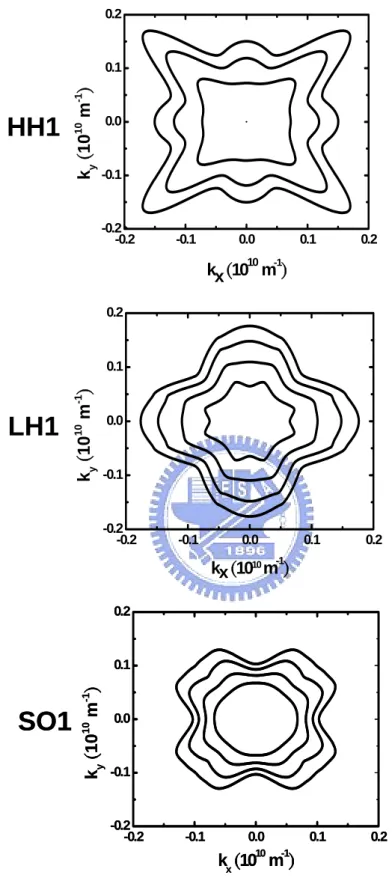
Fig. 3.9 The constant energy contours in a polar coordinate representation for the subbands HH1, LH1, and SO1.
Fig. 3.10 Constant energy contours of the HH1, LH1 and SO1 band at VBgB-VBfbB=-3.0V. The constant energy lines are separated by 25meV.
p.30
Fig. 3.11 Constant energy contours of the HH1, LH1 and SO1 subbands for (a) (001) and (b) (110) substrate at Vg-Vfb=-3.0V. The constant energy lines is 25meV. Only one spin state is plotted for clarity.
p.31
Fig. 3.12 Density-of-states of Si (001) and (110) substrates. EB0B is the
minimum of the lowest subband.
p.32
Fig. 3.13 The hole density distribution for different gate bias. p.33 Fig. 3.14 The inversion hole charge as a function of gate bias. p.34 Fig. 3.15 ZBavgB of the inversion layer as a function of gate bias. p.35
Fig. 3.16 The hole density distributions on (001) and (110) Si substrates at VBgB-VBfbB=-3.0V.
p.36
Fig. 3.17 ZBavgB of the inversion layer as a function of gate bias on (001) and
(110) Si substrates.
p.37
Fig. 4.1 Schematic section of the simulated structures; left: double gate MOS, right: single gate MOS.
p.42
Fig. 4.2 Inversion charge density profile within the silicon layer of a double gate MOS with Tsi=10nm, Tox=6nm, for three different bias points above threshold.
p.43
Fig. 4.3 Influence of the silicon thickness on the hole density distribution at the same VBgB-VBfbB.
p.44
Fig. 4.4 The dependence of the total hole density in the symmetrical DG device on the different silicon thickness.
Fig. 4.6 The inversion hole density as a function of gate bias in a DG and SG device with Tsi=20nm and Tox=3nm.
p.47
Fig. 4.7 The hole density distribution of a DG device is compared to that of a SG device with Tsi=20nm and Tox=3nm biased with the same gate drive.
p.48
Fig. 4.8 Transverse electric field within the upper half of the silicon layer of a DG structure and a SG one.
p.49
Fig. 5.1 Schematic section of the simulated structures: Ge and SiGe quantum well.
p.57
Fig. 5.2 Two dimensional density of states in Ge and SiGe quantum well. p.58 Fig. 5.3 Hole velocity and average energy versus electric field. p.59 Fig. 5.4 The phonon-limited low-field mobility in SiGe quantum well
structure.
p.60 Fig. 5.5 Comparisons of phonon-limited low-field mobility in Ge and SiGe
quantum well.
p.61
Fig. 5.6 Temperature dependence of the phonon-limited mobility in Ge quantum well.
Chapter 1
Introduction
For the past decades, the scaling of silicon complementary metal-oxide semiconductor (CMOS) transistor has enabled not only an exponential increase in integration circuit density, but also a corresponding enhancement in the transistor performance. But as the transistor gate length shrinks down to 35nm [1.1, 1.2], physical limitations, such as off-state leakage current and power density, make geometric scaling an increasingly challenging task. Therefore, new techniques are required to improve transistor’s performance. The key feature to enhance 90-, 65-, and 45-nm technology nodes is uniaxial-process induced stress [1.3-1.5]. For p-type MOSFETs, the embedded SiB1-xBGeBxB in source and drain area was promoted by Intel
[1.6]. For the counterpart of n-type MOSFETs, a tensile silicon nitride-capping layer was used to enhance electron mobility. However, for further CMOS scaling, it is imperative to investigate other high mobility channel materials, such as Ge, strained Si/Ge and GaAs [1.7, 1.8], which may possess better carrier transport property than a highly strained Si. As we know, the device performance can be affected through the band structure, which determines the scattering rates and density of states. As a consequence, the purpose of this thesis is to understand the band structure characteristics of these devices, especially for the case of complicated valence bands. In addition, carrier mobility can be further improved in quantum structure MOSFETs owing to the modification of a band-structure and carrier scattering rates. The valence subband structures of various devices, such as Ge quantum well, Si metal-oxide-semiconductor structure and double gate devices, are included in this
The organization of the thesis is in the following.
In chapter 2, the valence band structures are calculated by using a Luttinger-Kohn model. The 30 Å infinite quantum well of Si and Ge are compared.
In chapter 3, we examine the main features of a two-dimensional hole gas confined near a Si and SiOB2B interface. The six-band Luttinger-Kohn model is used to
study the band warping of the heavy-hole, light-hole and split-off bands. Moreover, we solve iteratively and simultaneously the Schrödinger and Poisson equations in the case of an inversion of holes in a P-channel metal-oxide-semiconductor structure for different gate biases. The simulated subband energies suggest that the use of one mass approximation in each subband is incorrect. Furthermore, the simulation results showed that the character of the subbands becomes mixed as the wave-vector kB//B
separates from zero. We also compare the main characteristics of the inversion layer on (001) and (110) substrates.
In chapter 4, the self-consistent solution of Schrödinger and Poisson equation is applied to single and double gate metal-oxide-semiconductor (MOS) structures. The influence of the semiconductor film thickness of the single and double gate MOS on the hole concentration distribution, inversion hole density, threshold voltage and transverse effective electric field is analyzed. The simulations results show that the transverse effective is lower in the double gate device compared to that in the single gate device, which possibly leads to improved mobility as a result of a reduction of the surface roughness scattering.
In chapter 5, we developed a two dimensional hole Monte Carlo simulation to study the hole transport in Ge and SiGe quantum wells. The intra and inter subband scattering rate are evaluated based on the Fermi-golden rule. The simulation results show that the phonon-limited low-field mobility in Ge quantum well is larger that that
temperature dependence of mobility is also demonstrated. Finally, a brief conclusion will be given in chapter 6.
Chapter 2
The Luttinger-Kohn Model
2.1 Introduction
Various methods have been developed to calculate a band structure in semiconductors. These methods can be grouped into four categories: the pseudopotential method [2.1,2.2], the envelope-function (k.p) method [2.3], the tight binding method [2.4], and the bond orbital model (BOM) method [2.5,2.6]. Among these methods, the pseudopotential approach is suitable for a conduction band structure and the k.p method is widely used to calculate a valence band structure. As a contrast, although the tight binding method can take the effect of a full valence band structure into account, the main disadvantage of this method is that it requires many empirical parameters which are usually determined by tedious fitting procedures. In this thesis, we calculate the valence band structure using the envelope function method. As we know, in the Kane’s model, as shown in Fig. 2.1 (a) and (b), only a conduction band, a heavy-hole, a light-hole and a split-off band with double degeneracy are taken into account. Other higher and lower bands are not considered, which results in an incorrect effective mass for the heavy-hole band. On the other hand, in the Luttinger-Kohn model, the heavy-hole, the light-hole and split-off bands in double degeneracy are considered and are called class A. All other bands are defined as class B. The effects of bands in class B on those in class A are included in the Luttinger-Kohn model.
In chapter 2, in order to take into account the effect of uniaxial compressive strain, the Luttinger-Kohn model is used. This model is similar to the k.p method.
The strain effects can be included with the Bir-Pikus deformation potentials. The Luttinger-Kohn model is described as follows.
2.2 Valence Band Structure Calculation
2.2.1 The Luttinger-Kohn Model
Based on the theory of Luttinger-Kohn and Bir-Pikus [2.7], the valence band structure of a strained bulk material can be derived by the following Hamiltonian in the envelope-function space:
1 3 3 0 2 , 2 2 2 3 1 3 , 0 2 2 2 2 3 1 3 , 0 2 2 2 2 1 3 3 0 2 , 2 2 2 1 2 3 2 0 1 1 , 2 2 2 2 1 1 3 1 , 2 2 0 2 2 2 2 LK P Q S R S R S P Q R Q S R P Q S S Q H R S P Q R S S Q S R P R S Q S P + + + + + + + + + + + + ⎡ + − − ⎤ ⎢ ⎥ ⎢ ⎥ ⎢ ⎥ − − − ⎢ ⎥ ⎢ ⎥ ⎢ ⎥ − − ⎢ ⎥ ⎢ ⎥ = − ⎢ ⎥ − + − − ⎢ ⎥ ⎢ ⎥ ⎢ ⎥ − − − + Δ ⎢ ⎥ ⎢ ⎥ ⎢ ⎥ − ⎢ − + Δ ⎥ ⎢ ⎥ ⎣ ⎦ where k P=P + Pε k Q=Q +Qε k R=R +Rε k S =S + Sε
2 2 2 2 2 0 ( ) ( 2 2 k x y Q k k m γ = = + − kz ) 2 2 2 2 3 0 ( ) 3 [- ( ) 2 2 k x y x y] R k k i k k m γ γ = = − + 2 3 0 ( ) 2 3 ( ) 2 k x S k m γ = = −ik k y z ( ) v xx yy zz Pε = −a ε +ε +ε ( 2 2 xx yy zz) b Qε = − ε +ε − ε 3 ( ) 2 xx yy xy Rε = − b ε −ε −idε ( zx yz) Sε = −d ε −iε
where is the spin△ -orbit splitting, γB1B, γB2B, and γB3B are the Luttinger parameters, and aBvB,
b, and d are the Bir-Pikus deformation potentials. The basis function represents the Bloch wave function at the zone center. The parameters used in this thesis are listed in Table 2.1.
| ,
J m
J>
1 3 ,3 ( ) 2 2 2 1 2 3 ,1 ( ) 2 2 6 3 1 2 3 , 1 ( ) 2 2 6 3 1 3 , 3 ( ) 2 2 2 1 1 1 ,1 ( ) 2 2 3 3 1 1 1 , 1 ( ) 2 2 3 3 X iY X iY Z X iY Z X iY X iY Z X iY Z − = + ↑ − = + ↓ + − = − ↑ + − = − ↓ = + ↓ + − = − ↑ − ↑ ↓ ↑ ↓2.2.2 Valence Band Structure of Bulk Si and Ge
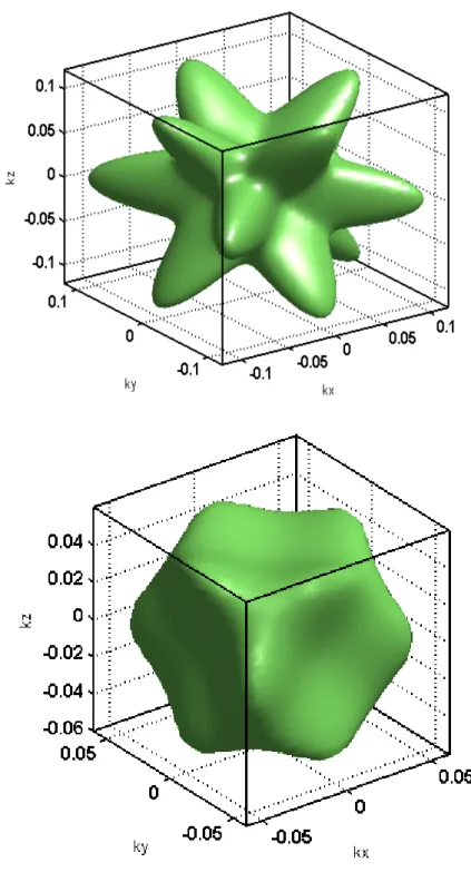
Si and Ge, respectively. The constant energy is 100 meV below the zone center. As shown in the figure, the heavy-hole band depicts the twelve promising prongs and the energy anisotropy for Ge is less severe than that for Si.
2.3 Subband Structures in Infinite Quantum Wells
When an external voltage is applied in the z-direction, the Schrodinger equation under the Luttinger-Kohn model is [2.10, 2.11]
6 6 , , , , ( , , ) ( ) ( ) ( , ) ( ) x y x y x y z n k k n x y n k k H k k k i qV z I z E k k z z × ϕ ϕ ∂ ⎡ = − + ⎤ = ⋅ ⎢ ∂ ⎥ ⎣ ⎦ where , ,
( )
x y n k kz
ϕ
is a 6x1 vector containing the components of the basis function,IB6x6B is the identity matrix of order 6, V(z) is the quantum confinement energy caused
by the external applied voltage, and EBnB is the subband energy of the n-th subband.
Since the system varies only along the z direction, and is translational invariant in the lateral directions. Then, we can express the Hamiltonian matrix element as a second-order polynomial in kBzB and replace the wave vector-component kBzB by the
operator kz= − ∂ ∂zi [2.12]. (2) 2 (1)( ) (0)( ) ij ij z ij z ij H =H ⋅k +H k& ⋅ +k H k& 2 (2) (1) (0) , , , , 2 [ ( )] ( ) ( x y x y n k k n x, )y n k k ( ) H iH H qV z z E k k z z z ϕ ϕ ∂ ∂ − − + + ⋅ = ⋅ ∂ ∂
Fig. 2.3 (a) and (b) show the comparison of hole subband structures calculated with the Luttinger-Kohn model and bond-orbital model for a 30 Å (001) infinite Si
<100> and <110> and confinement direction is taken to be along the z direction. Two points are worth noting. First, the Luttinger-Kohn model can yield reliable results only near the valence band maxima, and it’s not appropriate for the high energy portion of a valence band. Second, Ge generally has small quantization masses compared to that of Si, resulting in larger energy separations. For instance, as shown in Fig. 2.3 (b), an energy separation of 0.1 eV between the first and second subband is obtained.
Class A
Class B
Class B
Class A
Class B
Class B
Class A
Class B
Class B
E
s=E
g0
E
p= -Δ/3
E
so= -Δ
E
s=E
g0
E
p= -Δ/3
E
so= -Δ
Fig. 2.1 (a) The kp method in Kane’s model. (b) The Luttinger-Kohn
model.
Table 2.1 Material parameters for Si and Ge, respectively.
1 2 3
Material Parameters Symbol Unit Si Ref. Ge Ref. Valence band structure 4.285 [2.8] 13.38 [2.8]
0.339 [2.8] 4.24 [2.8] 1.446 [2.8] 5.69 [2.8] Spin-orbit splitt γ γ γ 0 ing eV 0.044 [2.8] 0.297 [2.8] Deformation potential eV 2.05 [2.9] 2.0 [2.9] eV 2.1 [2.9] 2.2 [2.9] eV 4.85 [2.9] 4.4 [2.9] Lattice constant 5.431 a b d a Δ − − − − 11 2 11 2 11 2 11 12 44 10 dyn/cm 10 dyn/cm 10 dyn/cm 5.646 Dielectric constant 11.7 16.0 Elastic constant c 16.577 [2.9] 12.853 [2.9] c 6.393 [2.9] 4.826 [2.9] c 7.962 [2.9] ε 6.680 [2.9] 1 2 3
Material Parameters Symbol Unit Si Ref. Ge Ref. Valence band structure 4.285 [2.8] 13.38 [2.8]
0.339 [2.8] 4.24 [2.8] 1.446 [2.8] 5.69 [2.8] Spin-orbit splitt γ γ γ 0 ing eV 0.044 [2.8] 0.297 [2.8] Deformation potential eV 2.05 [2.9] 2.0 [2.9] eV 2.1 [2.9] 2.2 [2.9] eV 4.85 [2.9] 4.4 [2.9] Lattice constant 5.431 a b d a Δ − − − − 11 2 11 2 11 2 11 12 44 10 dyn/cm 10 dyn/cm 10 dyn/cm 5.646 Dielectric constant 11.7 16.0 Elastic constant c 16.577 [2.9] 12.853 [2.9] c 6.393 [2.9] 4.826 [2.9] c 7.962 [2.9] ε 6.680 [2.9]
Fig. 2.2 Constant energy surfaces of the heavy-hole hand for (a) Si
and (b) Ge with energy 100meV below the zone center.
LK BOM
0.2
0.1
0.0
0.1
0.2
-0.1
-0.4
-0.3
-0.2
Subband
E
nerg
y
(
eV
)
Silicon
K
y=0
k
x=k
y LK BOM0.2
0.1
0.0
0.1
0.2
-0.1
-0.4
-0.3
-0.2
Subband
E
nerg
y
(
eV
)
LK BOM0.2
0.1
0.0
0.1
0.2
-0.1
-0.4
-0.3
-0.2
Subband
E
nerg
y
(
eV
)
Silicon
K
y=0
k
x=k
y LK bom0.2
0.1
0.0
0.1
0.2
-0.4
-0.3
-0.2
Su
bb
and
E
n
e
rgy
(eV
)
Germanium
k
y=0
k
x=k
y LK bom0.2
0.1
0.0
0.1
0.2
-0.4
-0.3
-0.2
Su
bb
and
E
n
e
rgy
(eV
)
LK bom0.2
0.1
0.0
0.1
0.2
-0.4
-0.3
-0.2
Su
bb
and
E
n
e
rgy
(eV
)
Germanium
k
y=0
k
x=k
yFig. 2.3 Hole subband structure for a 30-Å (001) infinite Si and Ge
quantum well. Calculation from the Luttinger-Kohn model is
compared with that from the bond-orbital model. Energy plotted
along wave-vector direction of <100> and <110>. Confinement
direction is taken to be along z direction.
Chapter 3
Valence Band Calculation in Silicon Inversion
Layer by a Self-consistent Approach
3.1 Introduction
The effective mass approximation has been widely applied to the electron quantization in silicon inversion layer. Although such a treatment has also been used for the hole case [3.1,3.2], this methodology will result in an incorrect valence subband structures due to the band-mixing of the heavy, light and split-off bands and thus lead to an incorrect carrier transport behavior. One of the methods to incorporate these effects is based on the diagonalization of the Luttinger-Kohn Hamiltonian in the framework of the effective mass theory [2.12, 2.13]. The strain effect can be easily incorporated into Luttinger-Kohn Hamiltonian by including the Bir-Pikus deformation potentials.
3.2 Device Configuration and Simulation Technique
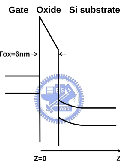
Fig. 3.1 shows the simulated one-dimensional (1D) Si–SiOB2B pMOS structure on
a 500nm (100) silicon substrate. The coupled Schrödinger and Poisson equation is solved by using the three-point finite difference method with a nonuniform mesh. 100 grid points for a 500 nm substrate are used to obtain well converged wavefunctions and subband energies. Furthermore, the linear 1D Poisson equation is solved by the Newton iteration scheme.
3.2.1 Formulation for the Schrödinger Equation
The formulation for the Schrödinger Equation had been described in chapter 2 and the corresponding equations are described as follows
6 6 , , , , ( , , ) ( ) ( ) ( , ) ( ) x y x y x y z n k k n x y n k k H k k k i qV z I z E k k z z × ϕ ϕ ∂ ⎡ = − + ⎤ = ⋅ ⎢ ∂ ⎥ ⎣ ⎦ (1) (2) 2 (1)( ) (0)( ) ij ij z ij z ij H =H ⋅k +H k& ⋅ +k H k& (2) 2 (2) (1) (0) , , , , 2 [ ( )] ( ) ( x y x y n k k n x, )y n k k ( ) H iH H qV z z E k k z z z ϕ ϕ ∂ ∂ − − + + ⋅ = ⋅ ∂ ∂ (3)
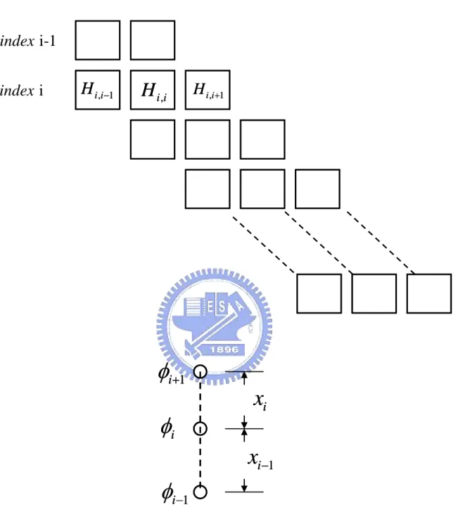
In this section, we mainly focus on the formulation of the Schrödinger Equation with a nonuniform mesh. Following by the approach given in [3.3], we firstly discretized the differential equation by using a three-point finite difference method. The index i represents each discretized lattice point and hBiB stands for the mesh size between
adjacent grid points xBiB and xBi+1B. This will give an asymmetric tridiagonal-block matrix
if the mesh spacings are nonuniform, as shown in Fig. 3.2 (a), which yields a 6NBz Bx
6NBzB eigenvalue problem. (2) (0) , 1 1 (1) (2) , 1 1 1 1 (1) (2) , 1 1 1 1 1 2 ( ) ( ) ( 1 2 2 ( ) ( ) ( 2 1 2 2 ( ) ( ) ( ) 2 i i i i i i i i i i i i i i i i i i i H H H V z h h h h iH H H h h h h h iH H H h h h h h − − − − − − + − − = + ⋅ + + + = − ⋅ + ⋅ + + = − ⋅ − ⋅ + + ) ) i (4)
This may be cast in the form of a matrix equation,
Here, we define the following parameters:
2 ( )
Li = hi +hi−1 / 2 (6)
Thus, the matrix becomes
' (2) (0) 1 , 1 (1) ' (2) , 1 1 (1) ' (2) , 1 1 1 { ( ) ( ( )) ( ) 2 1 { ( ) } 2 1 { ( ) } 2 i i i i i i i i i i i i h h B H H V z h h iH B H h iH B H h − − − − + } + = + + + ⋅ = − + = − − (7) We set 2 ij i ij B =L H
Then it can be easily shown that instead of solving Eq. (5), one can solve Eq. (8) to obtain the eigenvalue λ corresponding to the eigenfunction Φ due to the symmetric and tridiagonal matrix A, which ensures the real-valued eigenvalues.
AΦ = Φ
λ
(8)where
A
=
L BL
−1 −1 andϕ
=L−1Φ3.2.2 Formulation for the Poisson Equation
The one dimensional Poisson equation taking position dependence of dielectric constant into consideration is expressed as
( ( )ε z φ( ))z q ( ( )p z n z( ) NA−( )z ND+( ))z
Where q represents elementary charge equal to 1.6x10P
-19
P coulomb, ε(z) is the
position-dependent dielectric constant in each material, and ( )φ z is the electrostatic
potential. In the simulation, complete ionization at 300K is assumed. In oxide region, Eq. (9) reduces to
2 ( ) 0
z φ
∇ = (10)
Discretization of Eq. (10) is given by
1 1 1
1 1
1
(
)
i i i ix
x
iφ
φ
+φ
− −=
+
Δ
where 11
1
(
i i)
x
x
−Δ =
+
and xBiB and xBi+1B are defined in Fig. 3.2 (b).In semiconductor region, discretization of Eq. (9) can be obtained first by linearizing Eq. (9), i.e. let φ(k+1) =φ( )k + , then δ
( ) ( ) ( ) k A D q n p q n p N N
ε
∇ ⋅∇ −δ
β
+ ⋅ =δ
− + − − ∇ ⋅∇ε
φ
(11) whereβ
=q kTAppling three-point finite difference method gives
1 1 1 1 1 1 1 1 1 2 1 2 1 ( ) ( ) ( ) ( ) i i i i i i i i i i i i i A D i i i i x x x x q n p q n p N N x x x x 1 δ δ δ δ φ φ φ φ ε β δ ε + − + − − − − − − − − − − − + = − + − − + + − i c (12) or bi−1δi−1+ +δi ai+1δi+1=
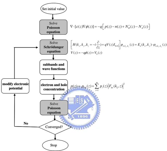
3.2.3 Flow Chart of Self-consistent Calculation
The simulation flow of the coupled self-consistent Schrödinger and the Poisson equation is shown in Fig. 3.3. First, we obtained the classical electrostatic potential distribution by solving the Poisson equation. Then, we get the corresponding subbands and wavefunctions by solving the Schrödinger equation according to Eq. (8). Here, we have defined an energy, EBlimB, to obtain the hole concentrations in the
continuum (pB3dB) and in the subbands (pB2dB). For energies below EBlimB the hole
concentration (pB3dB) is evaluated as an incomplete Fermi integral [3.4] by using a
continuous distribution of the density of states. For energies above EBlimB, the subband
energies are calculated and the two-dimensional hole concentration is calculated by Eq. (13) [3.4]. * 2 2 2 , ( ) ln(1 exp( i Fp)) ( ) d j i j E E m kT p z z kT ϕ π − =
∑
⋅ + = (13)With the new
φ
( )
z
, and using Eq. (3) and (9), we calculate p(z) once again, and continue iteratively until convergence is obtained. For a particular gate bias, this method allows us to obtain the band structure in the kBxB-kByB plane, the distribution of thepotential due to the external voltage along the z direction of the device, and the two-dimensional hole concentration in each subband.
3.3 Simulation Results
The simulated structure is shown in Fig. 3.1, where we have depicted the potential distribution of pMOS. The applied bias, VBgB-VBfbB, is changed from -1.5 to 4.0
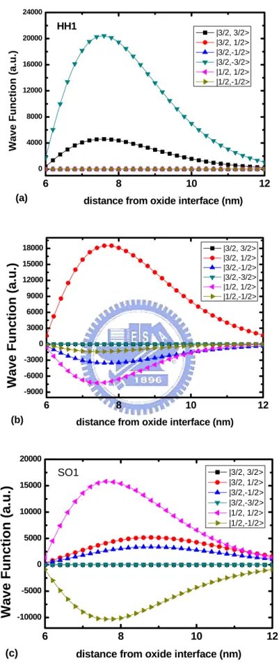
Fig. 3.4 and Fig. 3.5 illustrates the components of the wavefunction for each subband and valence band structure on (001) Si substrate with applied bias VBgB-VBfbB=
-3.0(V) at Γ point k=[0,0], respectively. Each subband is composed of six basis functions, 3 3
2 2
| ,
± >
(heavy hole states), 3 12 2
| ,
± >
(light hole states), and1 1
2 2
| ,
± >
(split-off states). The labels of the subbands are defined from the characteristic basis states at the zone center. For example, HH1 denotes the first heavy-hole subband, in which the two heavy-hole basis functions 3 32 2
| ,
± >
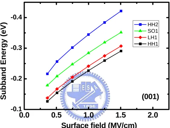
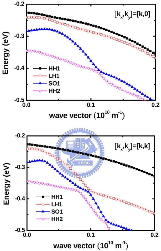
are dominant. Likewise, LH1 is the first light-hole subband, SO1 is the first split-off subband. Fig. 3.6 shows the subband energies as a function of the surface field on (001) Si substrate. Note that the heavy hole-like subband is the ground state. The calculated subband structures along two principal directions, [kBxB,kByB]=[k,0] and [k,k],are also plotted in Fig. 3.7. Fig. 3.8 demonstrates the wavefunction percentage of the HH1 subband along [kBxB,kByB]=[k,0.5k]. The characteristic of the subband becomes
mixed as the kB//B is separated from zero. From Fig. 3.7 and Fig. 3.8, it should be noted
that the intersubband transition energy is strongly affected by the band-mixing effect. Fig. 3.9 shows constant energy contours represented by the polar coordinates for the subbands HH1, LH1 and SO1. The strong band-mixing effect results in a warping of the constant energy contour. The constant energy contours for the HH1, LH1 and SO1 subbands are illustrated in Fig. 3.10 and the constant energy lines are separated by 25meV. Apparently, the effective mass varies in different directions. For this reason, an analytical form is inadequate and the numerical tabular form for the subband structure is needed to perform the Monte Carlo simulation. Fig 3.11 (a) and (b) shows the constant energy contours of various subbands on (001) and (110) Si substrate, respectively. It can be seen clearly that the density of states of (110) Si substrate is smaller that that of (001) Si substrate due to smaller available k states
between E and E+△E. Furthermore, Fig. 3.12 shows the calculated density of states
as a function of energy on (001) and (110) Si substrate according to [3.5]
2 2 0 2 ( ) (2 ) k k D E d E π θ π = ∇
∫
Lower density of states on (110) substrate compared to that on (001) suggests that the implementation of (110) substrate for the device’s active layer will be useful in achieving a high mobility channel [3.6].
Fig. 13 shows the two-dimensional hole concentration distribution for different gate bias for a 6nm oxide thickness. Apparently, the peak of the hole concentration is decreased as the gate bias is decreased. On the other hand, the distance corresponding to the peak hole concentration is shorter with larger gate bias. The inversion hole density is also shown in Fig. 14. Fig. 15 shows the behavior of inversion layer centroid, ZBavgB, as a function of gate bias, where ZBavgB is defined as
( ) ( ) Si avg Si p z z dz Z p z dz ⋅ ⋅ = ⋅
∫
∫
(14)Our simulation has obtained a ZBavgB between 2.48nm and 1.84 nm for VBgB-VBfbB= -1.5
and -4 V, respectively. ZBavgB has been shown to be an important parameter in electron
modeling [3.7] and it is also expected to be similar in the hole confinement. Moreover, to assess the importance of several scattering mechanisms as interface roughness and coulomb scattering, precise calculations of ZBavgB are needed to determine the distance
Finally, we compared the hole concentration distributions on (001) and (110) Si substrate with same applied gate bias. Fig. 16 shows that the peak depth of the hole concentration on (110) Si substrate is closer to SiOB2B/Si interface than on (001) Si,
which implies clear difference in (110) and (001) inversion layer thickness. It can be easily realized from the fact that for the bulk Si band structure, (110) surface yields a larger quantization mass, which will suffer larger confinement effect. As a result, a larger confinement effect results in smaller ZBavgB, which leads to smaller inversion
layer thickness. The comparison of ZBavgB on (001) and (110) Si substrate is also shown
in Fig. 17. The calculated ZBavgB on (110) is 1nm thinner than that on (001) for VBgB-VBfbB=
-3.0 V, which implies that in terms of inversion layer capacitance, the (110) pFETs show higher performance than (001) pFETs [3.8].
Oxide
Gate
Si substrate
Tox=6nm
Z=0
Z
, i i
H
, 1 i iH
−H
i i, 1+ , i iH
, 1 i iH
−H
i i, 1+i
index
i-1
index
ix
1 ix
− iφ
1 iφ
+ 1 iφ
− ix
1 ix
− iφ
1 iφ
+ 1 iφ
−Fig. 3.2 (a) Tridiagonal block matrix for the Schrodinger equation. (b)
Discretization of the potential using a nonuniform mesh.
Set initial value Solve Poissson equation Solve Schrödunger equation subbands and wave functions
electron and hole concentration Solve Poissson equation modify electronic potential Stop Converged? No
Set initial value
Solve Poissson equation Solve Schrödunger equation subbands and wave functions
electron and hole concentration Solve Poissson equation modify electronic potential Stop Converged? No 2 3 1 ( ) ( ) ( ) ( , ) m d i i i p z p z p z Fα k z = = +
∑
& [ ( )ε z φ( )]z q p z( ) n z( ) ND( )z NA( )z + − ⎡ ⎤ ∇ ⋅ ∇ = − ⎣ − + − ⎦ 6 6 , , , , ( , , ) ( ) ( ) ( , ) ( ) ( ) ( ) ( ) x y x y x y z n k k n x y n k k h H k k k i qV z I z E k k z z V z q z V z ϕ ϕ φ × ∂ ⎡ = − + ⎤ = ⋅ ⎢ ∂ ⎥ ⎣ ⎦ = − +Fig. 3.3 Flowchart of self-consistent calculation by solving the
Schrödinger and the Poisson equations.
6 8 10 12 0 4000 8000 12000 16000 20000 24000 W a ve Function (a.u.)
distance from oxide interface (nm)
|3/2, 3/2> |3/2, 1/2> |3/2,-1/2> |3/2,-3/2> |1/2, 1/2> |1/2,-1/2> HH1 (a) 6 8 10 12 -9000 -6000 -3000 0 3000 6000 9000 12000 15000 18000 (b) |3/2, 3/2> |3/2, 1/2> |3/2,-1/2> |3/2,-3/2> |1/2, 1/2> |1/2,-1/2>
Wave Function (a.u.)
distance from oxide interface (nm)
6 8 10 12 -10000 -5000 0 5000 10000 15000 20000 (c) |3/2, 3/2> |3/2, 1/2> |3/2,-1/2> |3/2,-3/2> |1/2, 1/2> |1/2,-1/2> Wave F u n ctio n (a.u .)
distance from oxide interface (nm)
SO1
Fig. 3.4 The components of the wave function at zone center for (a)
HH1, (b) LH1, and (c) SO1.
6
12
-0.50
-0.25
0.00
18
HH2
SO1
LH1
Energy (eV)
Distance from Gate (nm)
HH1
Fig. 3.5 The calculated valence band structure on (001) Si substrate.
The V
BgB-V
BfbB= -3.0V. The n-type substrate doping is 5*10
P17
P
cm
P-3
0.0
0.5
1.0
1.5
2.0
-0.1
-0.2
-0.3
-0.4
Subband Energy (eV)
Surface field (MV/cm)
HH2 SO1 LH1 HH1(001)
Fig. 3.6 The energies of the subbands as a function of the surface field
on (001) Si substrate
B.0.0 0.1 0.2 -0.5 -0.4 -0.3 -0.2 HH1 LH1 SO1 HH2
Ener
gy (eV)
wave vector
(
10
10m
-1)
[
k
x,k
y]
=[k,0]
0.0 0.1 0.2 -0.5 -0.4 -0.3 -0.2[
k
x,k
y]
=[k,k]
HH1 LH1 SO1 HH2Ener
gy (eV)
wave vector
(
10
10m
-1)
Fig. 3.7 The subband structures along two principal directions for 2D
holes on (001) Si substrate at V
BgB-V
BfbB=-3.0V.
0.0
0.5
1.0
1.5
2.0
2.5
0.0
0.2
0.4
0.6
0.8
1.0
Percentage
k
//(10
9m
-1)
% of heavy hole % of light hole % of split-offFig. 3.8 Nature of the 1st subband on (001) Si substrate.
B.BThe
0 10 20 30 40 50 60 70 80 90 0.00 0.05 0.10 0.15 0.20 0.25 0.30 90 meV |k|
(
10 10 m -1)
θ (degree) 10 meVHH1
0 10 20 30 40 50 60 70 80 90 0.00 0.05 0.10 0.15 0.20 10 meV 90 meV |k|(
10 10 m -1)
θ (degree)LH1
0 10 20 30 40 50 60 70 80 90 0.05 0.10 0.15 10 meV 90 meV |k|(
10 10 m -1)
θ (degree)SO1
HH1
-0.2 -0.1 0.0 0.1 0.2 -0.2 -0.1 0.0 0.1 0.2 k y ( 10 10 m -1 ) kx (1010 m-1)LH1
-0.2 -0.1 0.0 0.1 0.2 -0.2 -0.1 0.0 0.1 0.2 k y ( 10 10 m -1 ) kx (1010m-1)SO1
-0.2 -0.1 0.0 0.1 0.2 -0.2 -0.1 0.0 0.1 0.2 k y ( 10 10 m -1 ) k x(10 10 m-1)SO1
-0.2 -0.1 0.0 0.1 0.2 -0.2 -0.1 0.0 0.1 0.2 k y ( 10 10 m -1 ) k x(10 10 m-1)Fig. 3.10 Constant energy contours of the HH1, LH1 and SO1 band.
The constant energy lines are separated by 25meV at V
BgB-V
BfbB=-3.0V.
-0.10 -0.05 0.00 0.05 0.10 -0.10 -0.05 0.00 0.05 0.10
k
y(
10
10m
-1)
k
x(
10
10m
-1)
HH1 LH1 SO1(001)
-0.10 -0.05 0.00 0.05 0.10 -0.10 -0.05 0.00 0.05 0.10k
y(
10
10m
-1)
k
x(
10
10m
-1)
HH1 LH1(110)
Fig. 3.11 Constant energy contours of the HH1, LH1 and SO1
subbands for (a) (001) and (b) (110) substrate at V
BgB-V
BfbB=-3.0V. The
constant energy lines is 25meV. Only one spin state is plotted for
clarity.
0 20 40 60 80 100 120 0.0 0.5 1.0 1.5 2.0 2.5 3.0 (110) (001) V g-Vfb= -3.0V DO S
(
10 15 eV -1 cm -2)
E-E0 (meV)Fig. 3.12 Density-of-states of Si (001) and (110) substrates. E
B0Bis the
0
2
4
0
1
2
3
Vg-Vfb= -2.0
Vg-Vfb= -2.5
Vg-Vfb= -3.0
Vg-Vfb= -3.5
Vg-Vfb= -4.0
Distance from Oxide (nm)
Ho
le Concen
trati
on
(
10
19cm
-3)
0
-1
-2
-3
-4
0
2
4
6
8
N
inv(
10
12cm
-2)
V
g-V
fb(Volt)
-1
-2
-3
-4
1.8
2.0
2.2
2.4
2.6
Tox=6nm
V
g-V
fbZ
avg(nm)
0
1
2
3
4
0.0
0.5
1.0
1.5
2.0
2.5
3.0
3.5
4.0
Hole Concentration
(
10
19cm
-3)
Distance from Oxide (nm)
(001)
(110)
Fig. 3.16 The hole concentration distributions on (001) and (110) Si
substrates at V
BgB-V
BfbB=-3.0V.
-1
-2
-3
-4
0.5
1.0
1.5
2.0
2.5
3.0
(001)
(110)
V
g-V
fbZ
av g(nm)
Fig. 3.17 Z
BavgBof the inversion layer as a function of gate bias on (001)
Chapter 4
Self-consistent Simulation of Quantization
Effects in Double Gate and Single Gate MOS
4.1 Introduction
The double-gate (DG) transistor, where the both gates are employed to control the channel, exhibits attractive advantages in comparison to the conventional MOS transistor. The double gate transistor has the properties of almost ideal subthreshold swing and high transconductance. The increase of DG transistor’s current is due to the formation of a double conducting channel close to the two Si and SiOB2B interfaces. The
additional advantage in terms of transconductance and current drive are attributed to the inversion layer of the silicon region away from the two interfaces, which suffer less surface roughness scattering. The double-gate transistor with even thinner semiconductor layer can work in the volume inversion regime [4.1-4.3], which means that the whole volume of the semiconductor region is in the strong inversion.
If the semiconductor layer is ultra thin, the energy quantization effect becomes evident which affects considerably the carrier distribution in the semiconductor and influences the transistor parameters. In this chapter, we firstly investigate the effect of the semiconductor thickness on the hole density distribution, threshold voltage and finally compare the double-gate and single-gate transistor in terms of hole density distribution and the effective electric field, which are related to the low field mobility.
(SG) MOS devices. The silicon thickness down to 5nm and the thickness of the back-oxide of the SG MOS device 50nm are considered. For the silicon layer, n-type doping with NBDB=10P
17
P
cmP
-3
P is assumed for both cases. The two gate electrodes of the
DG device and the front gate of the SG are assumed of pP
+
P-polysilicon, while in the
SG device a grounded nP
+
P-polysilicon gate mimics the effect of the silicon substrate,
as shown in Fig 4.1.
The simulation is carried out by self-consistently solving the Poisson and Schrödinger equations. The quasi-Fermi levels for electrons and holes are set within the whole simulation domain, to reflect a bias condition with grounded source and drain. The poly depletion and wave function penetration into the gate oxide are neglected in our simulations. The procedures of solving the Poisson and Schrödinger equations are referred to chapter 3.
4.3 Results and Discussions
4.3.1 Symmetric Double Gate MOS
Fig. 4.2 shows the hole concentration distribution in a DG MOS device with 10nm silicon thickness and 6nm oxide, which is biased above threshold. A maximum at the center of the silicon layer is obtained at lower gate voltage, while at higher gate voltage two inversion maxima are formed. The effect of volume inversion vanishes rapidly as silicon thickness is increased, resulting in a reduction of the minority carrier concentration in the middle of the silicon layer.
Fig. 4.3 shows the influence of the silicon thickness on the hole concentration distribution at the same VBgB-VBfbB. As shown in Fig. 4.3, if the silicon thickness is
from the classical picture. In Fig. 4.4, the dependence of the total inversion hole density on the different silicon thickness in the symmetrical DG device is shown. For the small VBgB-VBfbB, i.e. small surface potential, when the potential is nearly rectangular,
the quantization is effective only for silicon thickness thinner than 20nm, as a result of the hole wave functions confinement by the two silicon and oxide interfaces. On the other hand, for the larger VBgB-VBfbB, all holes are confined in the surface subwells. As a
consequence, the inversion hole density does not depend on the silicon thickness. Fig. 4.5 shows the dependence of the threshold voltage on the silicon thickness TBsiB. The threshold voltage is determined by the linear extrapolation of the gate voltage
dependence of the inversion hole density [4.4]. It is worth noticing that the turn-around characteristic of the threshold voltage is demonstrated, which implies that for silicon layer thickness below 20nm, the effects of surface inversion layer overlap and the hole energy quantization become obvious. On the other hand, an appropriate work function of the double gate should be chosen to adjust the positive threshold voltage of pFET demonstrated here.
4.3.2 Comparison of Double Gate and Single Gate MOS devices
In this section, we will focus on the advantages of DG devices in comparison to SG devices in terms of the low-field mobility, which is determined by the transverse electric field in the silicon layer and the displacement of the peak hole concentration from the oxide interface.
In Fig. 4.6, the inversion hole density as a function of the gate voltage in a DG and SG MOS device with 20nm silicon thickness and 3nm oxide is shown. The inset is the linear scale of the inversion hole density versus the gate voltage to extrapolate the threshold voltage. Both two devices show ideal subthreshold swing, which is
in SG device due to the formation of the two conducting channels. In Fig 4.7 (a), the hole concentration distribution of a DG device is compared to that of a SG device biased with the same gate drive, which means the difference of the threshold voltage of the two devices is considered. The calculated inversion hole density is 7.32*10P
12
P
cmP
-2
P for a DG device and 3.65*10P
12
P
cmP
-2
P for a SG device, respectively. The inversion
hole density of a DG device is twice of a SG device. As shown in the Fig. 4.7 (b), the DG inversion hole density distribution is more displaced from the interface than the SG one, which is about 0.45nm. This difference is crucial in determination of the low-field mobility. Finally, Fig. 4.8 compares the transverse electric field within one half of the silicon layer of a DG and a SG device biased at the same gate drive. The transverse electric field is lower in the DG device and vanishes at the middle of the silicon layer due to the symmetry of the structure. Moreover, the surface roughness scattering rate is given by [4.5],
2 2 * 2 2 2 2 2 ( ) / 2 2 2 2 0 3 ( ) ( ) 2 2 k L SR eff eff m L e k L k e I E E s
π
ε
− Δ Γ = ∝ Δ ⋅ =where △ is the average displacement of the interface and EBeffB is the effective electric
field. In a consequence, the effective electric field is lower in the DG device, which possibly results in the improved mobility as a result of a reduction of the surface roughness scattering.
oxide oxide
P
+-poly
P
+-poly
Front Gate
Back Gate
oxide oxideP
+-poly
P
+-poly
Front Gate
Back Gate
oxide oxideP
+-poly
N
+-poly
Front Gate
Back Gate
oxide oxideP
+-poly
N
+-poly
Front Gate
Back Gate
Fig. 4.1 Schematic section of the simulated structures; left: double
gate MOS, right: single gate MOS.
6 8 10 12 14 16 0 1 2 3 4 5 6 V g-Vfb= -1.6V Vg-Vfb= -1.3V Vg-Vfb= -1.0V
Hole Concentration
(
10
18cm
-3)
Distance (nm)
Fig. 4.2 Hole concentration profile within the silicon layer of a double
gate MOS with Tsi=10nm, Tox=6nm, for three different bias points
above threshold.
6
12
18
24
30
3
0
2
4
6
Hole Concentr
ation
(
10
18cm
-3)
distance from oxide (nm)
si_5nm si_10nm si_20nm si_30nm
V
g-V
fb= -1.1
N
D=10
17(
cm
-3)
Fig. 4.3 Influence of the silicon thickness on the hole concentration
distribution at the same V
BgB-V
BfbB.
-0.7
-0.8
-0.9
-1.0
-1.1
-1.2
-1.3
10
810
910
1010
1110
12Tsi 5nm
Tsi 10nm
Tsi 20nm
Q
inv(
cm
-2)
V
g-V
fb(Volt)
Fig. 4.4 The dependence of the total inversion hole density in the
symmetrical DG device on the different silicon thickness.
0 10 20 30 0.10 0.05 0.00 -0.05 -0.10
Threshold Voltage (Volt)
Silicon Thickness (nm)
T ox=3nm N D=10 17(
cm-3)
Fig. 4.5 The dependence of the threshold voltage on the silicon layer
thickness,Tsi.
-0.7
-0.8
-0.9
-1.0
-1.1
-1.2
-1.3
10
710
810
910
1010
1110
1210
13Q
in v(
1/
cm
2)
V
g-V
fb(Volt)
DG
SG
Tsi=20nm
Tox=3nm
-0.7 -0.8 -0.9 -1.0 -1.1 -1.2 -1.3 0 2 4 Qin v ( 10 12 cm -2 ) Vg-Vfb (Volt) DG SG Tsi=20nm Tox=3nm-0.7
-0.8
-0.9
-1.0
-1.1
-1.2
-1.3
10
710
810
910
1010
1110
1210
13Q
in v(
1/
cm
2)
V
g-V
fb(Volt)
DG
SG
Tsi=20nm
Tox=3nm
-0.7 -0.8 -0.9 -1.0 -1.1 -1.2 -1.3 0 2 4 Qin v ( 10 12 cm -2 ) Vg-Vfb (Volt) DG SG Tsi=20nm Tox=3nmFig. 4.6 The inversion hole density as a function of gate bias in a DG
and SG device with Tsi=20nm and Tox=3nm.
5 10 15 20
0.0 0.5
1.0 Single Gate SOI Double Gate
Hole C
onc
entra
tion
(
10
19cm
-3)
Distance (nm)
T si=20nm T ox=3nm 4 6 0.0 0.2 0.4 0.6 0.8 1.0 1.2Single Gate SOI Double Gate
Ho
le Co
ncentratio
n
(
10
19cm
-3)
Distance(nm)
T si=20nm T ox=3nmFig. 4.7 The hole density distribution of a DG device is compared to
that of a SG device with Tsi=20nm and Tox=3nm biased with the
same gate drive.
4 6 8 10 12
0.0
0.2
0.4
0.6
0.8
Transverse
Ele
c
tr
ic
Field
(MV
/cm)
Distance (nm)
Single Gate SOI Double Gate T si=20nm T ox=3nm
E
eff
=387kV/cm
E
eff
=339kV/cm
4 6 8 10 120.0
0.2
0.4
0.6
0.8
Transverse
Ele
c
tr
ic
Field
(MV
/cm)
Distance (nm)
Single Gate SOI Double Gate T si=20nm T ox=3nm
E
eff
=387kV/cm
E
eff
=339kV/cm
Fig. 4.8 Transverse electric field within one half of the silicon layer of
a DG device and a SG one.
Chapter 5
Hole Transport in Si/Ge Quantum Well
5.1 Introduction
Currently, uniaxial compressively strained Si is the dominant technology for high performance pMOSFETs. For further CMOS scaling, it is imperative to investigate other high mobility channel materials, such as Ge and strained Si/Ge, which may possess better carrier transport property than a highly strained Si.
Due to drastic changes in carrier transport theory as CMOS is scaling down beyond 45nm, the traditional device simulator is inadequate to correctly predict the device’s performance, such as FinFet, double gate, SOI and so on. As a result, the first principle of the transport theory, Boltzmann transport equation, is needed. The purpose of this chapter is to study the hole transport properties based on the Monte Carlo method. Since the hole scattering rate is closely associated with a hole wave function and a subband structure, the hole mobility may change significantly with the shape of the Si/Ge quantum well geometry. Thus, to obtain a structure-dependent scattering rate, realistic subband structure and hole wave-functions are used in the evaluation of the scattering rate. Tabular forms of the subband E-k structure and scattering rates are established in our Monte Carlo simulation.
5.2 Physical Model and Simulation Technique
Two important scattering mechanisms are considered in the simulation: acoustic phonon scattering and optical phonon scattering. The scattering-matrix elements are approximated, such that phonon scattering can be considered as velocity randomizing.
The square of the matrix elements between the m-th subband and the n-th subband [5.1]: 2 2 2 3 m 2 2 3 1 ( , ') ( , , ) I , ( , ', ) 2 mn D D x y z D n D z z M k k M q q q k k q dq
π
=∫
×Where MB3DB is the corresponding matrix element for a bulk hole and q is a phonon
wave vector. The overlap integral IBmnB is defined as
m 2
I , ( , ', )n D k k qz Fnα( , )k z Fmα( , )exp(k z iq z dzz )
α ∗
=
∑∫
The coupling coefficient for the two dimensional hole is derived:
2 m 2
1
( , ')
I , ( , ', )
2
( ', )
( ', )
( , )
( , )
mn n D z z n n m mH
k k
k k q
dq
F
αk
z F
βk
z F
αk z F
βk z dz
α βπ
∗ ∗=
=
∫
∑∑
∫
Using the matrix elements, the two dimensional hole scattering rates are calculated according to [5.2]. The acoustic phonon scattering rate is give by
2 ' 2 2 ( ) ( , ) B ac n mn l k T S D E H u π ρ Ξ = ⋅ ⋅ k k
where Ξ is the effective acoustic deformation potential, ρ is the material density, uB1 Bis
the sound velocity, T is lattice temperature and DBnB(E) is the two dimensional density
![Fig. 3.8 Nature of the 1st subband on (001) Si substrate. B . B The wave-vector is along [kB x B , k B y B ]=[k, 0.5k] at V B g B -V B fb B =-3.0V](https://thumb-ap.123doks.com/thumbv2/9libinfo/8622130.191612/39.892.168.726.323.749/fig-nature-subband-si-substrate-wave-vector-b.webp)