This content has been downloaded from IOPscience. Please scroll down to see the full text.
Download details:
IP Address: 140.113.38.11
This content was downloaded on 25/04/2014 at 07:28
Please note that terms and conditions apply.
Structural and optical properties of buried InAs/GaAs quantum dots on GaAsSb buffer layer
View the table of contents for this issue, or go to the journal homepage for more 2009 J. Phys. D: Appl. Phys. 42 185106
(http://iopscience.iop.org/0022-3727/42/18/185106)
J. Phys. D: Appl. Phys. 42 (2009) 185106 (5pp) doi:10.1088/0022-3727/42/18/185106
Structural and optical properties of
buried InAs/GaAs quantum dots on
GaAsSb buffer layer
Y H Wu
1, Li Chang
1, P Y Lin
2, C H Chiang
3, J F Chen
3and T W Chi
4 1Department of Materials Science and Engineering, National Chiao-Tung University, Hsinchu 30050,Taiwan, Republic of China
2Industrial Technology Research and Development Master Program on Semiconductor Materials and
Processing, National Chiao-Tung University, Hsinchu 30050, Taiwan, Republic of China
3Department of Eletrophysics, National Chiao-Tung University, Hsinchu 30050, Taiwan, Republic of
China
4Electronics and Optoelectronics Research Laboratories, Industrial Technology Research Institute,
Hsinchu 30050, Taiwan, Republic of China E-mail:[email protected]
Received 15 May 2009, in final form 24 July 2009 Published 4 September 2009
Online atstacks.iop.org/JPhysD/42/185106 Abstract
In this work, we investigated the effect of a 1 nm thick GaAs94.3Sb0.57buffer layer on structural
and optical properties of buried InAs quantum dots (QDs) and wetting layers (WLs) in GaAs using photoluminescence (PL) and transmission electron microscopy (TEM). The density and emission wavelength of the QDs on the buffer were increased due to the size and the shape modification in comparison with those without a buffer. PL analysis of the ground-state (GS) peak of the QDs on the buffer showed a red-shift of 18 meV with an enhanced intensity. In addition, PL and TEM show that the buffer has a weak effect on the WLs and no apparent changes occur for the buffer during QD deposition and the capping process.
(Some figures in this article are in colour only in the electronic version)
1. Introduction
The synthesis of self-assembled quantum dots (QDs) has attracted much attention in the past two decades, owing to its unique properties for technological applications and scientific studies. The optical properties of QDs can be modified sensitively by varying materials, dimensions and structures from various processing conditions. Self-assembled InAs QDs via the Stranski–Kratanow (SK) growth mechanism due to lattice mismatch are one of the most attractive systems, which have been a candidate of long-wavelength lasers in infrared ranges, especially for vertical cavity surface emitting lasers [1,2]. Recent studies on InAs QDs show that fabrication of structures for long-wavelength emission with a homogeneous QD density and size is possible to realize its application for optical devices. One of the approaches for self-assembly of homogeneous InAs QDs often used is to apply a capping layer of compositions different from GaAs on QDs to obtain various
structural and optical properties [3,4]. Alternatively, a buffer layer can be deposited prior to QD deposition during which QDs formation may be changed due to the effects of the surface energy and strain field [5,6].
Harmand et al indicated that with the assistance of antimony as a surfactant it is possible to obtain smooth interfaces of a 9 nm-thick quantum well and extend the range of emission wavelength [7]. Influences of Sb incorporation on the density, shape and luminescence of InAs dots had been reported in detail by Chen et al [8]. For Sb incorporation into the buffer layer, Yamaguchi et al first demonstrated that the surface density of InAs QDs on a 1 monolayer (ML) GaSb buffer layer grown by MBE can reach about 1× 1011cm−2 from atomic force microscopy (AFM) observation [9]. Similar observations have been shown for InAs QDs on a 7 nm thick GaAs0.98Sb0.02 buffer layer
with enhanced PL intensity by Shimizu and Saravana [10]. Guimard et al illustrated that the increased density of surface
J. Phys. D: Appl. Phys. 42 (2009) 185106 Y H Wu et al
InAs QDs with enhanced photoluminescence (PL) intensity can be achieved by antimony-surfactant-mediated growth in metal organic chemical vapour deposition (MOCVD) [11]. They also indicated that no red-shift occurred when antimony was introduced before the InAs growth step. Generally, previous studies on QDs had shown that increase in the QD density reduces the average volume of QDs with a blue-shift of photoemission. However, it is still not clear about the role of the Sb-containing buffer layer on the structural and optical properties of buried InAs QDs and the wetting layer (WL). Furthermore, the buried InAs QDs have practicable use due to easy packaging for technological applications nowadays. Buffer layers of dilute antimony compositions can have direct influences on the initial formation of dots in various degrees. In this study, we present the structural and optical properties of buried InAs QDs on a GaAs94.3Sb5.7
buffer layer in GaAs from transmission electron microscopy (TEM) and PL characterization, showing that the red-shifting of PL emission with enhanced intensity has resulted from the increase in the QD size with modified shape. Further, the unusual modification of the QD’s properties can be shown to be attributed to the 1 nm buffer layer of low surface energy material.
2. Experimental details
The QD nanostructures were deposited on a n+ GaAs (0 0 1)
substrate by solid source molecular beam epitaxy in a Riber machine. A 0.3 µm-thick GaAs layer with doped 6.0 × 1016cm−3 Si was first deposited onto the substrate
with a growth rate of 3 Å s−1 at 600◦C. A nominal 10 Å GaAs0.943Sb0.057buffer layer, supplied from a Sb cracker, was
then deposited with a growth rate of 3 Å s−1 at 600◦C. The GaAsSb composition was deduced from high-resolution x-ray diffraction measurements of the lattice parameter on a 100 nm thick sample deposited with the same condition. Deposition of 2.4 ML of InAs (equal to 7.2 Å) was performed at a growth rate of 0.28 Å s−1 (∼0.09 ML s−1)and at a substrate temperature of 485◦C without interruption. Finally, a 0.3 µm-thick GaAs capping layer with Si doped to 6.0× 1016cm−3 was grown
on QDs with a growth rate of 3 Å s−1at 600◦C. The structural characterization of QDs at the atomic scale was performed in a JEOL-2010F transmission electron microscope with a Gatan Tridiem energy filter with a 2k× 2k UltraScan frame transfer charge-coupled device (CCD) and a scanning transmission electron microscope (STEM) mode (about 1 nm probe size) with a high-angle annular dark field (HAADF) detector. For the [0 0 1] plan-view and [0 1 0] cross-sectional TEM specimen preparation, mechanical grinding and polishing were used to thin a specimen to about 500 nm thickness, followed by Ar+ milling at 4 kV with a low incident angle. Further, chemical polishing treatment was carried out to remove the surface amorphous layer on the TEM specimens for improving the HRTEM image observations. A double-frequency yttrium– aluminium garnet (YAG) : Nd laser at 532 nm was employed for the measurements of PL with a closed-cycle He cooling system. The laser beam size was focused to be about 1 mm in diameter.
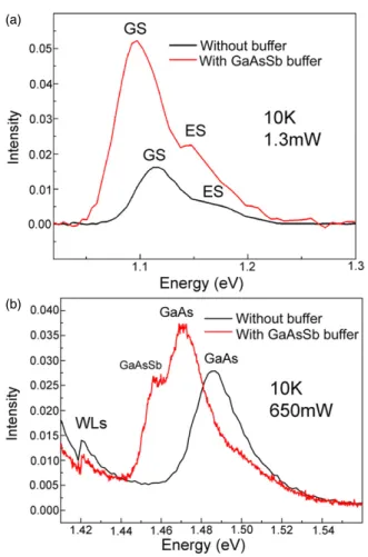
Figure 1. Low-temperature PL spectra of InAs/GaAs QD structure
without and with GaAsSb (red line) buffer layer at 10 K. (a) under an excited power of 1.3 mW. The GS and the first ES peaks are marked in each spectrum. (b) Under an excited power of 650 mW for showing high-energy emissions. (Colour online.)
3. Results and discussion
Figure 1(a) shows the PL spectra of the samples with and without the buffer under an excitation power of about 1.3 mW at 10 K. The ground-state (GS) and the first excited-state (ES) transitions of dots in each spectrum are displayed at two emission peaks which can be fitted with a Gaussian distribution. As can be seen in figure1(a), the PL peak position of GS from the conventional structure without the buffer is at 1.113 eV with a full-width at half maximum (FWHM) of 34.5 meV, and the ES peak is at 1.159 eV with a FWHM of 57.8 meV. The emission characteristics are similar to those QDs formed by deposition of 2.4 ML InAs on the GaAs matrix which have been previously shown in many studies [12–14]. For the case of QDs with the GaAsSb buffer layer, the GS and ES emission peaks with intensity enhancement are at 1.095 eV (FWHM of 35.8 meV) and 1.142 eV (FWHM of 69.9 meV), respectively. Thus, the red-shift of about 18 meV has clearly resulted from the effect of the GaAsSb buffer layer. It is possible that the QDs with the buffer have modified structural characteristics from those without the buffer. In figure1(b), the PL spectra were obtained from the low-temperature and high-excitation conditions. A weak peak can be seen in each spectrum at the same energy of 1.42 eV which has often been observed in InAs/GaAs QD structures and can be ascribed to 2
a thin WL [15–17]. As the WL peak in both cases is located at the same energy, it is suggested that they have similar chemical composition which is roughly estimated to be In0.2Ga0.8As
[17]. The strong and asymmetrical peak at the high-energy side in both cases is located at 1.471 eV and 1.486 eV for QDs with and without the buffer, respectively, with the emission range from 1.443 eV to 1.540 eV. These peaks are actually from the GaAs emission which has been shifted from 1.52 eV normally observed for bulk GaAs at 10 K probably due to the radiated heating of the GaAs surface by the high-power laser up to∼100 K. Moreover, a weak and broadening peak (around 1.454 eV) close to the GaAs peak in the spectrum of buried QDs with the buffer could have resulted from the thin GaAsSb buffer layer, in comparison with the PL spectrum without the buffer in which no such peak is present. It should be noted that though the GaAs surface has been heated up to 100 K, the WL and the buffer with the deep GaAs still remain at low temperatures as evidenced by the tail of the GaAs extended to 1.54 eV. It has been reported that the bandgap of bulk GaAs0.95Sb0.05at 10 K
is close to 1.413 eV. Hence, it is reasonable for 1 nm GaAsSb to increase the energy to 1.454 eV, if we take into consideration the effect of quantum confinement similar to the quantum well structure [18]. Therefore, it is believed that the GaAsSb buffer remains without significant change after deposition of InAs and GaAs capping, so that the intermixing of antimony plays no important role in QD formation. For intermixing of antimony, the annealing temperature at 750◦C is required for a weak diffusion phenomenon to occur, as shown by Khreis et al [19]. Also, it has been suggested that there is no significant Sb incorporation within the InAs QDs grown on GaAs : Sb [11]. In this work, the highest deposition temperature of the two samples was 600◦C for about 1000 s, which might not be able to give an appreciable thermal diffusion at the atomic scale. Further evidence is from the fact that the WLs in both cases have the same peak energies, suggesting that no Sb mixing with the WL occurred during the InAs deposition.
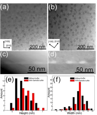
Further characterization of structural properties supports the above PL results. Plan-view bright-field scanning transmission electron microscopy (BF-STEM) along the [0 0 1]GaAszone axis in figure2(a) shows that the QD density
without the buffer is 3.5× 1010cm−2, and it increases to
5.5× 1010cm−2with the GaAsSb buffer in figure2(b). The
increase in density up to about 54% also evidences that no diffusion of Sb into the dot structure occurs as it has been shown that InAs QDs with dilute Sb incorporation may reduce the density [8]. Figures2(c) and (d) show the cross-sectional STEM-HAADF images along the [0 1 0]GaAszone axis which
were collected on an annular detector of scattering angle ranging from 90 to 180 mrad. The contrast of HAADF images is sensitive to atomic number and relatively insensitive to strain, such that In-rich areas appear brighter. Figures2(e) and (f ) illustrate the size statistics of QDs without and with buffer, respectively. From the measurements of the QDs in plan-view and cross-sectional images, the QDs in both cases exhibit similar shape, which is close to a truncated pyramid. The QDs grown without the buffer have an average height of 5.2± 1 nm and a width of 13.6 ± 1 nm, while the use of the GaAsSb buffer layer increases the dimension of the
Figure 2. Plan-view bright-field STEM images from InAs/GaAs
QD structure without (a) and with (b) GaAsSb buffer layer in the [0 0 1] zone axis. Cross-sectional HAADF images in the [0 1 0] zone axis of QDs (c) without and (d) with GaAsSb buffer layer.
Histograms showing the distribution of the dots size for height (e) and base width (f ) measured from cross-sectional HAADF images and plan-view BF-STEM images, respectively.
dots to a height of 5.6± 1 nm and a width of 13.0 ± 1 nm on average. Comparison of the average height and width in statistical histograms for both cases illustrates the modified aspect ratio of buried InAs QDs from 0.38 to 0.43. The shape change may result in a red-shift of the GS peak of the QDs with buffer, as shown by Ngo et al in a theoretical study on the effects of size and shape on the electronic states of QDs, which indicated that the elongation of the wavelength of GS follows sensitively the aspect ratio of QDs, and the height of the pyramid-shaped dots gives a heavy response than width in the smaller aspect ratio which should be smaller than 0.8 [20]. Figure3shows the HRTEM observation of two pyramid-shaped dots along the [0 1 0] zone axis without digital image processing. Based on the distinguishable lattice features and strain contrast, the edge shape of QDs is depicted as the white line. The height of the dots from the HRTEM observation of the conventional sample in figure3(a) is 3.5± 0.5 nm, slightly less than 4.2± 0.5 nm of QDs with the GaAsSb buffer layers in figure2(b). It is remarkable for the larger contact angle of 41◦for InAs QDs on the GaAsSb buffer compared with 35◦for QDs without the buffer. Following this direct observation, it is likely that the larger contact angle of QDs is due to the lower surface energy of the buffer layer containing Sb. As the lattice mismatch of the GaAsSb buffer with GaAs is about 0.1%, the critical thickness is estimated to be more than 300 nm, such that the 1 nm thick buffer layer is in the pseudomorphic region where the strained GaAsSb has the same in-plane lattice as GaAs at the interface. Thus, the surface energy of the buffer layer as surfactant may play a major role in the InAs QD
J. Phys. D: Appl. Phys. 42 (2009) 185106 Y H Wu et al
Figure 3. Cross-sectional HRTEM images on the [0 1 0] zone axis of edged QDs for 2.4 ML InAs deposited. Height of InAs dots is (a) with
a GaAs buffer layer of about 3.5 nm and (b) with a GaAsSb buffer layer of about 4.2 nm.
Figure 4. [0 1 0] zone axis HRTEM images of WLs (a) without and
(b) GaAsSb buffer layer after digital image processing. The regions of different lattice feature of WLs are marked with arrows.
formation. The surface energy of GaAsSb is lower than that of GaAs [21,22]. A similar phenomenon, which shows the increase in density and aspect ratio of surface Ge islands during Ga-surfactant-mediated deposition on Si, has been shown by Portavoce et al [23].
The structural properties of active nanostructures in the self-assembled QDs formed by SK growth mode are also sensitive to the formation of the WLs. To extract the information of WLs directly, HRTEM examination has been performed on the WL without the buffer and on the GaAsSb buffer layer, as shown in figures4(a) and (b), which clearly display the lattice feature after Wiener-filter digital image processing, respectively. The image processing reduces the effect of noise to improve the HRTEM quality of WLs with an enhanced lattice feature. The WL without the buffer layer, as indicated by the two white arrows in figure 4(a), has a thickness of about 1.9± 0.5 nm. For the QDs with the buffer,
detailed examination of figure4(b) by geometric phase analysis identifies two different lattice features from the matrix GaAs as indicated by the white arrows. One corresponds to the buffer of about 1.5± 0.5 nm, while the other is the WL of about 1.8± 0.5 nm. The HRTEM results of the WL and the buffer support the interpretation of PL spectra in figure1(b).
4. Summary
In summary, the results of PL and TEM show that the effect of a 1 nm GaAsSb buffer layer on capped InAs/GaAs QDs is to modify the density and aspect ratio of QDs, resulting in the red-shift and intensity increase of the GS peak, whereas it has a weak effect on the WL.
References
[1] Stranski I N and Krastanow L 1938 Sitzungsber. Akad. Wiss.
Wien, Math. -Naturwiss. Kl. Abt. 2B 146 797
[2] Chow W W, Choquette K D, Crawford M H, Lear K L and Hadley G R 1997 IEEE J. Quantum Electron.33 1810
[3] Lian G D, Yuan J, Brown L M, Kim G H and Ritchie D A 1998 Appl. Phys. Lett.73 49
[4] Chang F Y, Wu C C and Lin H H 2003 Appl. Phys. Lett.
82 4477
[5] Akahane K, Kawamura T, Okino K, Koyama H, Lan S, Okada Y, Kawabe M and Tosa M 1998 Appl. Phys. Lett.
73 3411
[6] Suzuki R, Miyamoto T, Matsuura T and Koyama F 2006
Japan. J. Appl. Phys.45 L585
[7] Harmand J C, Li L H, Patriarche G and Travers L 2004 Appl.
Phys. Lett.84 3981
[8] Chen J F, Chiang C H, Wu Y H, Chang L and Chi J Y 2008 J.
Appl. Phys.104 023509
[9] Yamaguchi K and Kanto T 2005 J. Cryst. Growth275 2269
[10] Shimizu H and Saravanan S 2006 Appl. Phys. Lett.
88 041119
[11] Guimard D, Nishioka M, Tsukamoto S and Arakawa Y 2006
Appl. Phys. Lett.89 183124
[12] Steer M J, Mowbray D J, Tribe W R, Skolnick M S, Sturge M D, Hopkinson M, Cullis A G, Whitehouse C R and Murray R 1996 Phys. Rev. B54 17738
[13] Koike K, Ohkawa H and Yano M 1999 Japan. J. Appl. Phys.
38 L417
[14] Bruls D M, Vugs J W A M, Koenraad P M, Salemink H W M, Wolter J H, Hopkinson M, Skolnick M S, Long Fei and Gill S P A 2002 Appl. Phys. Lett.81 1708
[15] Sanguinetti S, Henini M, Grassi Alessi M, Capizzi M, Frigeri P and Franchi S 1999 Phys. Rev. B60 8276
[16] Pohl U W, P¨otschke K, Schliwa A, Guffarth F, Bimberg D, Zakharov N D, Werner P, Lifshits M B, Shchukin V A and Jesson D E 2005 Phys. Rev. B72 245332
[17] Hugues M, Teisseire M, Chauveau J M, Vinter B, Damilano B, Duboz J Y and Massies J 2007 Phys. Rev. B76 075335
[18] Quochi F, Kilper D C, Cunningham J E, Dinu M and Shah J 2001 IEEE Photon. Technol. Lett.13 921
[19] Khreis O M, Homewood K P, Gillin W P and Singer K E 1998
J. Appl. Phys.84 4017
[20] Ngo C Y, Yoon S F, Fan W J and Chua S J 2006 Phys. Rev. B
74 245331
[21] Liu W, Zheng W T and Jiang Q 2007 Phys. Rev. B75 235322
[22] Lee J P, Jang Y J and Sung M M 2003 Adv. Funct. Mater.
13 873
[23] Portavoce A, Kammler M, Hull R, Reuter M C, Copel M and Ross F M 2004 Phys. Rev. B70 195306
![Figure 4. [0 1 0] zone axis HRTEM images of WLs (a) without and](https://thumb-ap.123doks.com/thumbv2/9libinfo/7916830.156687/5.892.112.401.360.755/figure-zone-axis-hrtem-images-wls.webp)
