國 立 交 通 大 學
電子工程學系 電子研究所碩士班
碩 士 論 文
低功率數位式自我校正鎖相迴路
低功率數位式自我校正鎖相迴路
低功率數位式自我校正鎖相迴路
低功率數位式自我校正鎖相迴路
Low Power Digital Phase Locked Loop with
Self-Calibration
研 究 生 : 張巧伶
指導教授 : 陳巍仁
低功率數位式自我校正鎖相迴路
低功率數位式自我校正鎖相迴路
低功率數位式自我校正鎖相迴路
低功率數位式自我校正鎖相迴路
Low Power Digital Phase Locked Loop with
Self-Calibration
研 究 生:張巧伶 Student : Chiao-Ling Chang
指導教授:陳巍仁 Advisor : Wei-Zen Chen
國立交通大學
電子工程學系 電子研究所 碩士論文
A Thesis
Submitted to Department of Electronics Engineering and Institute of Electronics College of Electrical and Computer Engineering
National Chiao-Tung University in Partial Fulfillment of the Requirements
for the Degree of Master
in
Electronics Engineering November 2008
Hsin-Chu, Taiwan, Republic of China
i
低功率數位式自我校正鎖相迴路
低功率數位式自我校正鎖相迴路
低功率數位式自我校正鎖相迴路
低功率數位式自我校正鎖相迴路
研究生: 張巧伶 指導教授:陳巍仁教授國立交通大學
電子工程學系電子研究所碩士班
摘要
摘要
摘要
摘要
頻率合成器(Frequency Synthesizer)對於通訊晶片,無論是無線射頻傳輸 介面或者高速的序列傳輸介面中,都扮演著非常重要的腳色,影響整個通 訊晶片的性能甚大。隨著製程的進步,深次微米(Deep-submicrometer)的互 補金氧半(CMOS)製程已廣泛地被應用於數位電路上,使得數位電路得以實 現高度密集化、低成本與低功率消耗等需求。類比電路在低電壓的環境下, 運作不易,不只增加設計上的難度,也使得類比電路無法隨著製程的演進, 降低功率消耗。近年來,有些研究紛紛提出了數位控制振盪器(Digital Controlled Oscillator)的概念,藉由數位訊號來控制振盪器的振盪頻率,其中 充電汞、迴路濾波器等的類比電路皆以數位電路取代,配合數位控制振盪 器,使得整個迴路得以全數位化,較易操作在低電壓的工作環境下,使整 體的功率能夠下降。本作品實現一個具有低功率數位式自我校正頻率合成器,使用聯電 90nm 1P9M 互補金氧半製程實現,且適用於生物感測器(Bio-sensor)上的收 發機(transceiver),中央頻率為 1.4GHz,預計功率消耗低於 1mW;相位雜 訊在距離載波頻率 1MHz 時小於-100dBc/Hz。此外, 為兼顧低功率操作與 性能穩定之雙重條件,本電路可依據 PVT 的變化自動調整硬體結構,以達 到自我校準與操作性能之最佳化。
iii
Low Power Digital Phase Locked Loop with Self-Calibration
Student: Chiao-Ling Chang Advisor: Wei-Zen Chen
Department of Electronics Engineering & Institute of Electronics
National Chiao-Tung University
Abstract
The frequency synthesizer is the key element use for both up-conversion and down-conversion of radio signals, and it also affects the performance of the whole transceiver. Along the progress of the deep-submicron CMOS process, the digital circuits could be implemented more integrative, and reduce the cost and the power consumption of the system. But analog circuits are difficult to operate with lower supply voltage and integrate with digital circuits. In the recent years, some researchers proposed the concept of the digital control oscillator (DCO), and the output frequency could be controlled by the digital codes. If we replace the charge-pump and the filter into digital loop filter, the whole PLL could be digitalized by replacing the charge-pump and the filter into digital loop filter, and the PLL could be operated with low voltage and lower down the power consumption.
This thesis proposes a low power digital phase locked loop with self-calibration circuits. The chip has been implemented in UMC 90nm 1P9M CMOS process and could be used on the transceiver of the Bio-sensor. The
center frequency of the RF output is 1.4GHz, and the expected phase noise at 1MHz offset is below -100dBc/Hz. The prospective total power consumption is lower than 1mW. A DCO calibration circuit is added to suppress the PVT variation and increase the stability of this loop.
v
致謝
致謝
致謝
致謝
感謝神終於等到這一刻了,歷經了一番掙扎,終於完成了這部拙作。 在此也感謝陳巍仁教授在這些日子以來,辛勤的教導與勉勵,才有現在的 成果,雖然有點久,但在學期間也學了不少的東西,獲益良多。謝謝我們 的大學長台祐,在這段期間的支持與協助。 在此還要感謝與我們同年的黃董、Lulu 裕和我的閃光-松諭,在這段艱 辛的時刻,一起共甘苦同患難。也感謝現在正在努力中的學弟們,科科、 宗恩、塔哥、歐陽等,在研究枯燥的期間帶來歡笑,感謝歐威大大在科專 計畫上的鼎力相助,不然我要忙翻了。在此也恭喜國維跟我們一起畢業。 謝謝碩二的學弟們,邱 99、小賴、育祥、順天、昕爺等常與我們一同談天 說地,也謝謝 Kitty 和彥緯開車陪我們一起去竹南棒線,讓我們免於頂著太 陽騎西濱。也謝謝新進的新血-書瑾、旻毅、文杰和健軒,為實驗室帶來歡 樂的氣氛。 最後感謝在背後支持我的家人,讓我安心的完成課業。 張巧伶 17, Nov, 2008Contents
摘要 摘要 摘要 摘要 ... i Abstract ...iii 致謝 致謝 致謝 致謝 ... v Contents... viList of Tables ...viii
List of Figures ... ix Chapter 1 Introduction ... 1 1.1 Motivation ... 1 1.2 Overview of Thesis... 4 Chapter 2 Architecture ... 5 2.1 Prior Art ... 5
2.2 Proposed Architecture of the Low Power ADPLL... 9
Chapter 3 Analysis of the ADPLL ... 12
3.1 The Dynamics of the ADPLL... 12
3.2 Linear Model of the ADPLL ... 13
3.2.1 Linear Model of the DCO ... 13
3.2.2 Linear Model of the Frequency Divider ... 14
3.2.3 Linear Model of the Bang-Bang PD ... 14
3.2.4 Linear Model of the Loop Filter ... 17
3.2.5 Linear Model of the Complete PLL Loop... 19
3.3 Generated Phase Noise ... 19
3.3.1 Noise Model of the DCO ... 19
3.3.2 Noise Model of the BBPD ... 28
vii
4.1 Phase Detector (PD) ... 32
4.2 Dynamic Loop Filter (DLF) ... 33
4.3 Calibration Digital Controlled Oscillator (CDCO) ... 35
4.3.1 Digital Controlled Oscillator (DCO) ... 35
4.3.2 DCO Calibration Circuit (DCC) ... 39
4.4 Frequency Divider ... 46
Chapter 5 Experimental Results ... 48
5.1 Layout and Chip Photo... 48
5.2 Experimental Setup ... 51
5.3 Experimental Results... 53
5.3.1 Open-Loop of the ADPLL ... 53
5.3.2 Closed-Loop of the ADPLL ... 58
5.4 Performance Summary ... 62 Chapter 6 Conclusion... 63 Reference ... 64 簡歷 簡歷 簡歷 簡歷 ... 66
List of Tables
Table 1-1 Specification of the proposed PLL ... 3
Table 4-1 The parameters of the analog filter ... 37
Table 4-2 The frequency range of the DCO with different corner... 39
Table 4-3 The gain estimation error with different condition in Fig. 4-21 ... 45
Table 5-1 The distribution of the poles and the zeros ... 56
ix
List of Figures
Fig. 1-1 WBAN concept... 1
Fig. 1-2 Architecture of the RF transceiver... 2
Fig. 2-1 Architecture of charge-pump PLL... 5
Fig. 2-2 Structure of Staszewski’s ADPLL [10] ... 7
Fig. 2-3 Architecture of Staszewski’s DCO [11]... 8
Fig. 2-4 Architecture of the proposed ADPLL... 9
Fig. 2-5 The distribution of power consumption in each building block in a PLL ... 10
Fig. 2-6 The concept of the DCO... 10
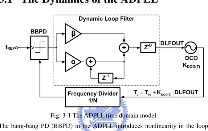
Fig. 3-1 The ADPLL time domain model ... 12
Fig. 3-2 The linearized model of the BBPD ... 14
Fig. 3-3 Markov chain approximating ... 16
Fig. 3-4 The linear model of BBPD in phase domain... 17
Fig. 3-5 z-domain model of the dynamic loop filter ... 17
Fig. 3-6 s-domain of the dynamic loop filter ... 18
Fig. 3-7 The linear model of the PLL loop ... 19
Fig. 3-8 The concept of the DCO... 19
Fig. 3-9 The noise model of the DCO architecture, excluding the DCO noise .. 20
Fig. 3-10 Nature noise spectrum of the oscillator... 23
Fig. 3-11 Quantization noise with different width m of the ∆Σ modulator, excluded analog filter ... 24
Fig. 3-12 Dithering noise with different oversampling rate fOS of the ∆Σ modulator, excluded analog filter... 25
Fig. 3-13 The output phase noise due to the ∆Σ modulator ... 26
Fig. 3-14 The output phase noise due to the ∆Σ modulator after analog filter ... 27
Fig. 3-15 The output phase noise spectrum of the DCO... 27
Fig. 3-16 The spectrum of the BBPD quantization noise ... 28
Fig. 3-17 The linear model of the ADPLL with noise sources ... 29
Fig. 3-18 The Bode plot of the open loop transfer function of the ADPLL ... 30
Fig. 3-19 The total output phase noise spectrum ... 31
Fig. 4-1 The structure of the phase detector (PD)... 32
Fig. 4-2 The architecture of the first D flip-flop ... 32
Fig. 4-3 The hysteresis diagram of the PD with different corner ... 33
Fig. 4-5 The waveform of the output of the integral path Ψ when stable... 34
Fig. 4-6 The process of the DGC ... 34
Fig. 4-7 The concept of the low power digital controlled oscillator... 35
Fig. 4-8 The architecture of the DCO ... 35
Fig. 4-9 The architecture of the IDAC ... 36
Fig. 4-10 The concept of the impedance scalar... 37
Fig. 4-11 The architecture of the ∆Σ modulator... 38
Fig. 4-12 The tuning curve of the DCO ... 38
Fig. 4-13 The transient response of the DCO with 1.4GHz RF output ... 39
Fig. 4-14 The relationship of the frequency to the different digital codes ... 40
Fig. 4-15 The concept of the DCO gain normalization... 40
Fig. 4-16 The concept of the DCO frequency offset calibration ... 41
Fig. 4-17 The process of the DCC... 42
Fig. 4-18 Control method of the DCC ... 42
Fig. 4-19 The architecture of the frequency detector... 43
Fig. 4-20 (a) The architecture of the synchronous counter (b) The time diagram of the first three bits ... 44
Fig. 4-21 The simulation results of the behavior model ... 45
Fig. 4-22 The architecture of the frequency divider ... 46
Fig. 4-23 The structure and the time diagram of the divide by 175... 47
Fig. 4-24 The post simulation results of the frequency divider with different corner... 47
Fig. 5-1 The layout of the ADPLL ... 48
Fig. 5-2 The floor plane of the analog circuits... 49
Fig. 5-3 The photograph of the whole chip... 50
Fig. 5-4 The evaluation board (a) AC board (b) DC board... 51
Fig. 5-5 The experimental setup... 52
Fig. 5-6 The tuning curve of the DCO ... 53
Fig. 5-7 (a) The spectrum of the RF output without the DSM with 100MHz frequency span (b) The spectrum of the RF output without the DSM with 500MHz frequency span (c) The phase noise of the RF output without the DSM ... 54
Fig. 5-8 (a) The spectrum of the RF output with the DSM with 100MHz frequency span (b) The spectrum of the RF output with the DSM with 500MHz frequency span (c) The phase noise of the RF output with the DSM ... 55
Fig. 5-9 The frequency response of the ideal and the implemented analog filter ... 56 Fig. 5-10 The phase noise of the DCO with different analog filter, excluding
xi
DCO nature noise ... 57 Fig. 5-11 The output of the frequency divider with 1.3 GHz and 1.7 GHz RF output frequency... 57 Fig. 5-12 (a) The spectrum of the RF output with 100MHz frequency span (b) The spectrum of the RF output with 500MHz frequency span (c) The phase noise of the RF output ... 58 Fig. 5-13 (a) The spectrum of the RF output with 100MHz frequency span (b) The spectrum of the RF output with 500MHz frequency span (c) The phase noise of the RF output with higher bias current of the analog filter ... 60 Fig. 5-14 After the DCC enabled, (a) The spectrum of the RF output with
100MHz frequency span (b) The spectrum of the RF output with 500MHz frequency span (c) The phase noise of the RF output with higher bias current of the analog filter... 61 Fig. 5-15 The power distribution of the ADPLL ... 62
Chapter 1
Introduction
1.1
Motivation
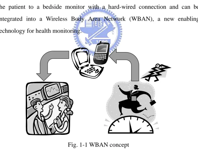
In the recent year, people could live over seventy years or longer. Health care has become a popular issue in the whole word. Recent technological advances in sensors, low-power microelectronics and miniaturization, and wireless networking enable the design and proliferation of wireless sensor networks capable of autonomously monitoring and controlling environments. A number of these devices has the advantage of allowing patient movement without tethering the patient to a bedside monitor with a hard-wired connection and can be integrated into a Wireless Body Area Network (WBAN), a new enabling technology for health monitoring.
Fig. 1-1 WBAN concept
The concept of WBAN is shown in Fig. 1-1. People can carry a tiny sensor all around without staying beside the monitor. The sensor could get vital signals, such as electrocardiogram (ECG), and transfer the relevant data to a personal
2
digital assistant (PDA) or a personal computer (PC) through a wireless personal area network implemented using ZigBee (802.15.4) [1] or Bluetooth (802.15.1) [2]. Those devices allow an individual to closely monitor changes in body’s vital signs which can provide feedback to help maintain an optimal health status, and these systems can even alert medical personnel when life-threatening changes occur.
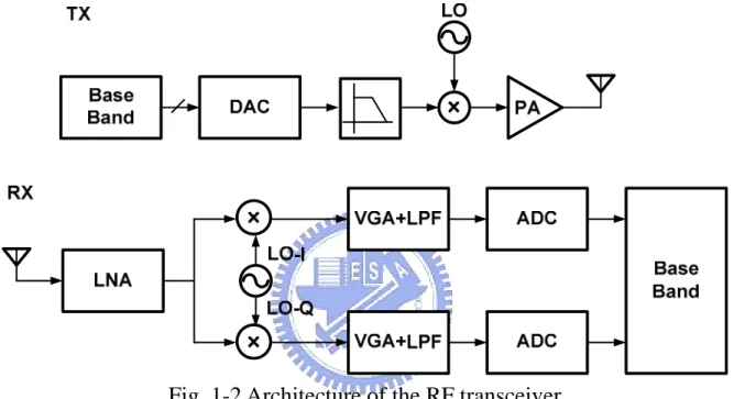
Fig. 1-2 Architecture of the RF transceiver
In this application, a radio frequency (RF) transceiver is necessary for delivering the signal between sensors and local hard ware. The architecture of the RF transceiver is shown in Fig. 1-2. The operation of transceiver is as following. Baseband signal converts to analog signal with a digital-to-analog converter (DAC). Up-conversion mixer mixes carrier frequency generated by local oscillator (LO) and analog signal filtered by low pass filter. The antenna of the transmitter (TX) transfers RF signal which is amplified with power amplifier (PA). The antenna of the receiver (RX) receives the RF signal and delivers to a low noise amplifier (LNA) to amplify the received signal. RF signal is converted to baseband signal with a mixer and LO. A variable gain amplifier (VGA) and
low pass filter (LPF) is used for amplifying the received signal and filtering the noise produced by higher frequency, and then the output baseband signal is converted to digital signal with an analog-to-digital converter (ADC).
Frequency synthesizer is a key element in transceiver and is generally implemented by phase-locked loop (PLL). A sub-µW PLL is necessary for reducing the power consumption of the whole system. The central frequency for ZigBee (IEEE 802.15.4) or Bluetooth is about 2.4GHz, which might be interfered by other application, such as 802.11 a, b, g. Federal Communication Commission (FCC) has voted to adopt new rules establishing a service for wireless medical telemetry devices [3]. The Wireless Medical Telemetry Service (WMTS) report and order sets aside the frequencies of: 1395 to 1400 MHz and 1429 to 1432 MHz for primary or co-primary use by eligible wireless medical telemetry users. This action creates frequencies where medical telemetry will enjoy protection against interference from other in-band RF sources and reduce power consumption by lower central frequency.
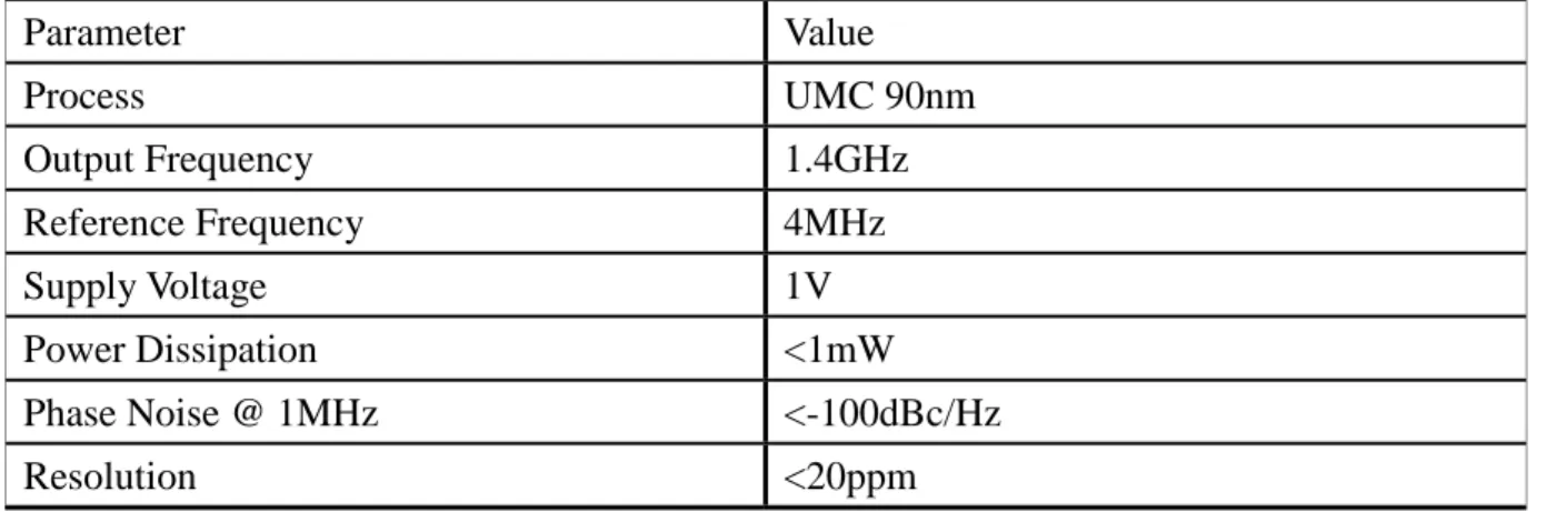
We propose a low power PLL with self-calibration in this thesis. The specification of this proposed PLL is shown in Table 1-1.
Table 1-1 Specification of the proposed PLL
Parameter Value Process UMC 90nm Output Frequency 1.4GHz Reference Frequency 4MHz Supply Voltage 1V Power Dissipation <1mW Phase Noise @ 1MHz <-100dBc/Hz Resolution <20ppm
4
1.2
Overview of Thesis
The organization of this thesis is as follows. In Chapter 2, we propose a new architecture of low power PLL. We give a behavior model and an analyze method for the new architecture in Chapter 3. We implement each block in Chapter 4. Experimental results are provided in Chapter 5 and this thesis is concluded following a discussion in Chapter 6.
Chapter 2
Architecture
2.1
Prior Art
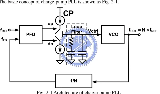
Emerging wireless sensor network applications call for radio architectures where size and current consumption are major design criteria. Many studies [4]-[6] have been carried out on frequency synthesizer based on a charge-pump PLL [7]. The basic concept of charge-pump PLL is shown as Fig. 2-1.
PFD VCO 1/N fREF fFB up dn
CP
Vctrl fOUT=
N × fREF Loop FilterFig. 2-1 Architecture of charge-pump PLL
In this architecture a voltage control oscillator (VCO) generates a periodic output signal having a frequency fOUT determined by a control voltage Vctrl. The output signal is divided by a frequency divider. The output frequency of the frequency divider fFB is fFB=fOUT/N, where N is the divide ratio and could be integer or fractional. A phase frequency detector (PFD) compares the phase or frequency of the feedback clock fFB against between reference frequency fREF. The information on the phase or frequency difference activates the charge-pump
6
of the VCO. A loop filter is used to reduce the noise formed by the CP. This loop locks when the phase difference drops to zero.
With the explosive growth of the processes, the use of deep-submicrometer CMOS processes allows for an unprecedented degree of scaling and integration in digital circuitry, but complicates the implementation of traditional RF and analog circuits. In the advance processes, the channel length of CMOS transistors becomes shorter to reduce the chip area, and the supply voltage of the circuits becomes lower to diminish the power consumption. The gate oxide of CMOS transistors gets thinner to enhance the driving strength in the advance processes. The current leakage of the transistors gets larger because of the thinner gate oxide that causes current mismatch in the CP. The range of the control voltage of the VCO shrinks because of the lower supply voltage that makes higher gain of the VCO. The VCO would be very susceptible to the noise of the control voltage that makes the VCO difficult to control.
Recently, a digitally controlled oscillator (DCO), which deliberately avoids any analog tuning voltage controls, was first ever presented in [8] for RF wireless applications. This allows for its loop control circuitry to be implemented in a fully digital manner. Staszewski develops an architecture of all-digital PLL (ADPLL) [9][10] which could integrate with digital circuitry. Fig. 2-2 shows the structure of Staszewski’s ADPLL [10].
Fig. 2-2 Structure of Staszewski’s ADPLL [10]
In Fig. 2-2, a digital control oscillator (DCO) generates a periodic signal CKV and feedbacks to an oscillator phase accumulator. The variable phase signal RV[i] is determined by counting the number of the rising clock transitions of the DCO oscillator clock. The reference phase signal RR[k] is obtained by accumulating by frequency command word (FCW) with every rising edge of the retimed frequency reference clock (CKR). FCW is the integer divide ratio of the target frequency to the reference frequency. A phase detector compares the difference of the sampled variable phase RV[k] and the reference phase RR[k] and gives an adjust signal which is conditioned by digital loop filter and modifies the output frequency of DCO. A time-to-digital converter (TDC) is used to increase the resolution of the phase error between reference clock and output signal. DCO gain normalization is needed to precisely establish the loop bandwidth. Because most of the circuits in this architecture are design in the digital manner, the ADPLL is easily implemented with the synthesis tool and is compatible with other digital circuits. In this way, the cost and the power consumption of the ADPLL could be shrunk with the development of CMOS process and integrated with digital circuitry.
8
Although many studies have been published concerning ADPLL, little attention has been paid to reduce power consumption in ADPLL. The DCO in ADPLL consumes about 25mW in a 90nm digital CMOS process [11] because of the LC oscillator. Fig. 2-3 is the architecture of the DCO which is controlled by varactor bank with digital codes. To diminish the power consumption of the DCO, the quality factor (Q) of the varactor needs to be high enough, and that is difficult to implement. If we use ring oscillator for DCO, we could lower the power consumption of the DCO, but the gain of DCO would be higher with lower supply voltage that makes DCO more sensitive to the noise.
Fig. 2-3 Architecture of Staszewski’s DCO [11]
In this thesis, we present a method to control a high gain DCO which could operate with low supply voltage. This study aims to present a low power ADPLL which could integrate with digital circuitry and oppose with process, voltage, and temperature (PVT) variation. The following section shows the proposed architecture of the low power ADPLL.
2.2
Proposed Architecture of the Low
Power ADPLL
Fig. 2-4 Architecture of the proposed ADPLL
The proposed architecture of all-digital PLL (ADPLL) is shown as Fig. 2-4. This architecture includes a calibration digital controlled oscillator (Calibration DCO), a frequency divider, a phase detector (PD), and a dynamic loop filter (DLF). The basic operation of the ADPLL is as following. The Calibration DCO generates a periodic clock and is divided by the frequency divider. The output frequency of the frequency divider is fOut/N. The phase detector compares the phase difference between reference frequency fRef and feedback clock fFB and delivers the adjust signal PDOUT to the DLF. The DLF produces the control code of the DCO to modify the output frequency of the DCO. The loop becomes stable when the output frequency fOUT is N times of reference frequency fREF.
The charge pump in conventional architecture is replaced by the DLF whish is composed with digital circuits and overcomes the non-idea effect in charge pump. The DLF also adds a mechanism to adjust the loop bandwidth automatically to shorten the acquisition time. The calibration DCO is used to oppose against the PVT variation and make the implemented loop transfer
10
function approach our target design. The detail description of the DLF and the calibration DCO is written in Chapter 4.
Divider 43% DLF 5% PFD 8% DCO 44%
Fig. 2-5 The distribution of power consumption in each building block in a PLL The distribution of power consumption in each building block of a PLL is illustrated in Fig. 2-5. In general speaking, the DCO uses almost half of total power consumption. If the power consumption of the DCO is reduced, the total power of the PLL would be decreased efficiently. From specification in Table 1-1 and the distribution of the total power, the power consumption of the DCO should be less than 450µW. The control current of the DCO has to be reduced to less than hundred micro watts to save more power, but the gain of the DCO might be higher that make the DCO difficult to control and sensitive to the noise on the control current or voltage.
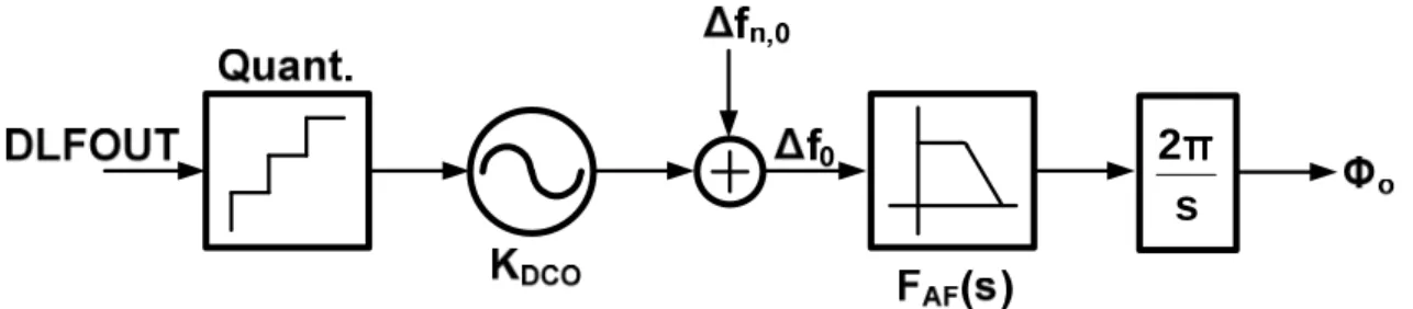
Fig. 2-6 The concept of the DCO
A ∆Σ modulator could provide high resolution, so we introduce a ∆Σ modulator to control a high gain DCO. The concept of the DCO is shown as Fig. 2-6. A filter is added at the output of the ∆Σ modulator to reduce the quantization
noise which is injected by the ∆Σ modulator. The width of the accumulator in the
∆Σ modulator decides the resolution of the DCO and the quantization noise
which would affect the phase noise performance of the DCO. To solve this problem, the effects of the bit number of the ∆Σ modulator and the bandwidth of the filter to the noise performance will be investigated in the following chapter.
12
Chapter 3
Analysis of the ADPLL
3.1
The Dynamics of the ADPLL
DCO KDCO(T) Frequency Divider 1/N
β
+
Z-1+
α
Dynamic Loop Filter
Z-D fREF DLFOUT K T Tv = v0+ DCO(T)⋅ DLFOUT BBPD
Fig. 3-1 The ADPLL time domain model
The bang-bang PD (BBPD) in the ADPLL introduces nonlinearity in the loop that invalidates the traditional Laplace domain analysis used in linear PLLs. Some researchers provide time domain analysis in the recent years [12]. The ADPLL time domain model is illustrated in Fig. 3-1, where Tv, D, and KDCO(T) mean the period gain of the DCO output, the total loop delay normalized to the period of reference clock fREF, and the gain of DCO which is expressed in equation 3.1. ( ) Code T K v T DCO ∆ ∆ = ( 3.1 )
According to his analyze, this loop would be stable when the parameters of the dynamic loop filter, β and α, fit in the following condition:
1 2 2 + < D β α ( 3.2 )
The architecture of the BBPD provides one clock delay which is described in section 4.1. To avoid the data racing in the DLF, one register is put between the DLF and the DCO, so that induces one clock delay. We assume the loop delay D as 2. The ratio of α to β must be less than 0.4, so let α=1 and β=8.
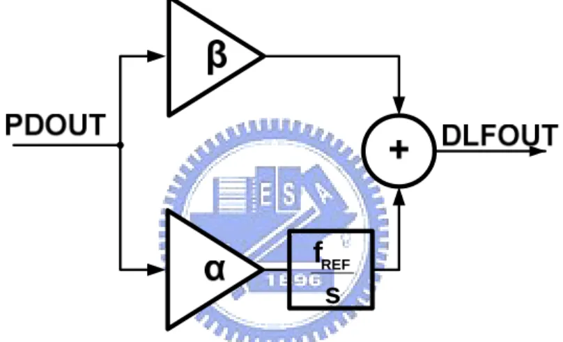
3.2
Linear Model of the ADPLL
The block diagram of the ADPLL can be shown as Fig. 2-4. The linear model of each block would be derived in the following section, and we would give a complete linear model of the PLL in section 3.2.5.
3.2.1
Linear Model of the DCO
The output frequency of the DCO could be varied according to the input code and it could be expressed as equation 3.3
( )
t f K DLFOUT( )
tfOUT = 1 + DCO× ( 3.3 )
, where f1 is the running frequency of the DCO, and KDCO is the gain of the DCO of which the unit is Hert/LSB. The angular frequency of the DCO could be derived as equation 3.4 which is rewritten by equation 3.3.
( )
t KDCO DLFOUT( )
tOUT =ω + π ×
ω 1 2 ( 3.4 )
The phase of the ωo(t) is
( )
∫
( )
∫
= + t DCO t OUT d 1t K 0DLFOUT d 0ω τ τ ω 2π τ τ o OUT φ φ φ = 1 +, where Φo is the excess phase of the output which could be written as
( )
DLFOUT( )
s s K s DCO o π φ = 214
3.2.2
Linear Model of the Frequency Divider
The relationship of the input and output of the frequency divider could be expressed in equation 3.5.
( )
t Nf( )
tfOUT = FB ( 3.5 )
From equation 3.5, the transfer function of the frequency divider could be derived as following.
( )
( )
s N f s f OUT FB = 1 ( 3.6 )3.2.3
Linear Model of the Bang-Bang PD
In this structure, the BBPD is the only nonlinear element and the gain Kbpd
depends on the jitter between the reference clock and the feedback clock. To model the behavior of the BBPD, Nicola derived the expression for the linearized gain of the BBPD with Markov chain theory [13]. If the rising edges
instants of the reference and the feedback clock are tr and td, the linearized
model of the BBPD could be illustrated in Fig. 3-2.
Fig. 3-2 The linearized model of the BBPD
In locked condition, the average value of the output of the BBPD must be zero.
[
PDOUT]
=0If the reference clock leads the feedback clocks, Δt>0, there will be more iterations with PDOUT=1, so that the average value of PDOUT will be positive, vice versa. It could be defined that the gain of the BBPD around the locked
condition as rate of change in E[PDOUT] with a small difference δ of the
probability density function (pdf) around the locked condition.
[
]
(
| =)
=0 ∂ ∂ ≡ δ E PDOUT difference δ δ Kbpd ( 3.7 )With the definition in equation 3.7, the gain of the BBPD could be derived as the following expression [13]
( )
0 2 tbpd f
K = ∆ ( 3.8 )
, where fΔt means the pdf of the time difference Δt.
Assume α<<β, the nonlinear map in presence of jitter tjr on the reference clock is the same as equation (5) in reference [12], exclude the loop delay D.
(
k D)
T DCO jr k k t t N K t t + =∆ + − ∆ − ∆ 1 β ( ) sgn ( 3.9 )If the values of Δt in case of unjittered reference isΔt *, Δt * can assume values on discrete states: nNβKDCO(T)+Δt 0
*
, where state number n is integer. From a given state n, Δt * might go either to state n+1 or state n-1, and the transition probabilities from state n to state n+1 is defined as G-n. If a given cumulative distribution function (cdf) of the jitter tjr is Ftjr(x)=P[tjr<x], the transition probability could be expressed as:
[
tk n tk n]
Ft(
nN KDCO( )T)
G n P jr − + ∈ + ∆ ∈ = − ≡ ∆ * * β 1 1| ( 3.10 )In section 3.1, the loop delay D is supposed to 2. From equation 3.9 the infinite Markov chain could be simplifies to a seven state chain which is
16
illustrated in Fig. 3-3, where the transition probability G2=G1=G0=G-1=G-2=0.5 and G3=1.
Fig. 3-3 Markov chain approximating
The stationary probability of occupancy of the state n is defined as qn which could be expressed as:
[
t n]
P
qn ≡ ∆ *∈
The stationary probability qn could be derived by the transition probability Gn [13]. 1 1 1 1 0 1 2 1 − ∞ = = − − + =
∑
∏
n n m m m G G q ( 3.11 )∏
= − − − = = n m m m n n q G G q q 1 0 1 1 ( 3.12 )From equation 3.11 and 3.12, we could find the stationary probability qn.
6 1 2 2 1 1 0 =q =q− =q =q− = q ( 3.13 ) 12 1 3 3 =q− = q ( 3.14 )
If tjr is Gaussian with variance σtjr 2
, then the equation 3.8 could be rewritten as the following: ( )
(
)
∑
=∞ −∞ = − = n n T DCO t n bpd q f nN K K jr β 2 ( 3.15 ) ( )(
)
( ) 2 2 1 2 1 − = − tjr T DCO jr jr K nN t T DCO t nN K e f σ β π σ β ( 3.16 )An approximate expression for Kbpd might be applied by equation 3.13-3.16 and could be shown as:
( ) ( ) ( ) + + + = − − − 2 2 2 5 . 4 2 2 1 3 1 3 2 3 2 3 1 2 1 tjr T DCO jr t T DCO jr t T DCO jr K N K N K N t bpd e e e K σ β σ β σ β π σ ( 3.17 )
From the linear model of BBPD in Fig. 3-2, the unit of the gain Kbpd is sec
-1
. To analyze this model in phase domain, the linear model of BBPD is redraw in Fig. 3-4.
Fig. 3-4 The linear model of BBPD in phase domain
The relationship between Kbpd and Kbpd(Φ) could be derived in equation
3.18. ( ) REF bpd bpd f K K π 2 = Φ ( 3.18 )
3.2.4
Linear Model of the Loop Filter
1 z 1 1 − −
18
Fig. 3-5 shows the z-domain model of the dynamic loop filter. The z operator is defined as fR
s
e
z= , where s= j2πf and 1/fR is the period of the sampling rate which is the same as the period of the reference frequency fREF in this design. We can make the following approximation:
REF f s f s e z = REF ≈ − − − 1 1 ( 3.19 )
Using equation 3.19, s-domain model of the dynamic loop filter could be illustrated in Fig. 3-6.
s fREF
Fig. 3-6 s-domain of the dynamic loop filter The transfer function of the dynamic loop filter could be written as:
( )
( )
( )
s
f
s
PDOUT
s
DLFOUT
s
F
=
=
β
+
α
REF ( 3.20 ) In the concept of the DCO in Fig. 2-6, the DCO includes a ∆Σ modulator and an analog filter. If the transfer function the analog filter is FAF(s), which is a low pass filter, those transfer functions could combine to the dynamic loop filter, and the total transfer function of the loop filter could be written as:( )
( )
( )
F( )
s s f s F s F s F AF REF AF ⋅ + = ⋅ = β α ' ( 3.21 )3.2.5
Linear Model of the Complete PLL Loop
s K 2ππππ DCO
Fig. 3-7 The linear model of the PLL loop
The linear model of the PLL loop is illustrated in Fig. 3-7, where Kbpd(Φ) and F’(s) are applied by equation 3.18 and 3.21.
3.3
Generated Phase Noise
3.3.1
Noise Model of the DCO
Fig. 3-8 The concept of the DCO
The concept of the DCO is shown in Fig. 3-8. A ∆Σ modulator is used to control the high gain oscillator, but the ∆Σ modulator might induce a quantization noise. An analog filter is added to cancel the noise caused by the ∆Σ modulator.
20
s
2ππππ
Fig. 3-9 The noise model of the DCO architecture, excluding the DCO noise The noise model of the DCO architecture is shown in Fig. 3-9, excluding the DCO noise. Since the input code spans multiple quantization levels, the DCO frequency quantization error is modeled in Fig. 3-9 as an additive uniformly-distributed random variable ∆fn,0 with white noise spectral characteristics. Another noise source is the nature noise caused by the DCO. The DCO noise spectrum affected by the ∆Σ modulator could be expressed as following.
( )
,0 , 2 2 n DSM n AF S f s s F SΦ = ⋅ π ∆ ( 3.22 )The noise spectrum of the random variable ∆fn,0 includes the quantization noise from finite frequency range and the dithering noise from noise-shaping by the
∆Σ modulator and could be written as:
dithering n quantize n n f f f S S S , , 0 , ∆ ∆ ∆ = +
Staszewski who proposed a digital controlled oscillator has provided the analytic method to design the DCO [11], but an analog filter is added in the architecture of the DCO in this thesis.
The variance of the adjust frequency ∆f0,quantize is
(
)
12
2 2 , 0 res ff
quantize∆
=
∆σ
( 3.23 )m T res f f 2 ∆ = ∆ ( 3.24 )
, where ∆fres is the frequency resolution, m is the width of the ∆Σ modulator, and
∆fT is the frequency tuning range of the DCO. The single-sided spectral density of the quantization noise ∆fn,quantize is
( )
REF f f f f S quantize quantize n 2 , 0 , ∆ ∆ ∆ = σ ( 3.25 ) From equation 3.23~3.25, the single-sided power spectrum density (PSD) to the output could be derived as equation 3.26 which multiplied by the sinc function corresponding the operation of the register (sample and hold).( )
(
)
(
)
2 2 2 2 2 sinc 1 12 1 2 2 2 , , f j F f f f f f S f j f j F f S AF REF REF res f AF nquantize quantize o ∆ ⋅ ∆ ⋅ ⋅ ∆ ∆ ⋅ = ⋅ ∆ ⋅ ∆ = ∆ ∆ ∆Φ π π π π ( 3.26 )The frequency step of the switching of the ∆Σ modulator is the frequency
tuning range ∆fT, so the variance of the dithering frequency is
( )
12 2 2 , 0 T f f dithering ∆ = ∆ σ ( 3.27 )The spectrum of the ∆Σ-shaped frequency deviation could be written as
( ) ( )
n OS OS T f f f f f f S dithering n 2 2 sin 2 1 12 , ∆ ⋅ ⋅ ∆ = ∆ ∆ ( 3.28 ), where fos and n mean the oversampling rate and the number of stages of the ∆Σ
22
( )
(
)
(
)
2 2 2 2 2 2sin 1 12 1 2 2 2 , , f j F f f f f f S f j f j F f S AF n OS OS T f AF ndithering dithering o ∆ ⋅ ∆ ⋅ ⋅ ∆ ∆ ⋅ = ⋅ ∆ ⋅ ∆ = ∆ ∆ ∆Φ π π π π π ( 3.29 )In 1999, few researchers presented the phase noise of the differential MOS ring oscillator [14]. The total power of the ring oscillator could be derived in the
equation 3.30, where N, Itail, and VDD mean the number of stages of the
oscillator, the tail current in each stage, and the supply voltage.
DD tailV
NI
P= ( 3.30 )
The frequency of the oscillation would be approximated as
(
max)
2 N C V I f node tail o η ≈, where η is the propagation constant, Cnode is the capacitance of the output node,
and Vmax is the maximum voltage swing of the output. The output noise of the
ring oscillator could be derived in equation 3.31, where k=1.38×10⁻²³ J/K is the
Boltzmann constant, T is the temperature in Kelvin degree, Vchar is the
characteristic voltage of the device, and RL is the load resistor.
( )
2 3 8 , ∆ ⋅ + ⋅ ⋅ ⋅ = ∆ Φ f f I R VDD V VDD P kT N f S o tail L char DCO n η ( 3.31 ) γ T GS char V V V = −From our specification in Table 1-1, the power consumption of the whole system is less then 1mW, so that the DCO has to operate under 400mA for 1V power supply. To reduce the power consumption of the DCO, the ring oscillator would be designed in three stages. If the power consumption of the ring oscillator is
about 100µW, the tail current of each stage has to be about 30µW. The phase noise caused by the ring oscillator circuits is pictured in Fig. 3-10.
104 105 106 107 108 109 -160 -140 -120 -100 -80 -60 -40 -20 0 Frequency (Hz) P h a s e N o is e ( d B c /H z )
Fig. 3-10 Nature noise spectrum of the oscillator
The total DCO noise spectrum density which is formulated in equation 3.22
could be rewritten in the following equation, where SΔΦnSDM and SΔΦo,quantize are
shown in equation 3.22. DSM n DCO n Total DCO n S S S , , _ , Φ Φ Φ = + ( 3.32 )
To reduce the affect of the quantization and dithering noise to the output, the
width of the ∆Σ modulator and the bandwidth of the analog filter should be
designed by equation 3.29 and 3.26 properly, and we let the output noise caused by those two factors less than the nature noise of the oscillator and the
specification. A 2nd order ∆Σ modulator is chose in this research. The signal
transfer function of the MASH (Multi-stage noise shaping) 1-1 ∆Σ modulator is
24
( )
1 2 1 1 − = − − ∆Σ z z z H ( 3.33 )Use the approximation in equation 3.19, the formula could be rewritten as
( )
12 − = ∆Σ s f s H OS ( 3.34 ), where fOS is the over sampling rate of the ∆Σ modulator.
If the tuning range of the oscillator is 30%, the frequency range of the oscillator is designed as 400MHz. From equation 3.26, the quantization noise to
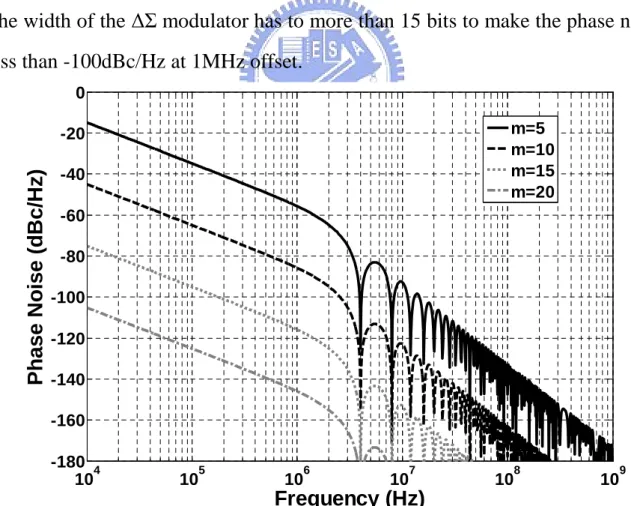
output could be lower with hither resolution of the ∆Σ modulator. Fig. 3-11
shows the expected phase noise spectrum caused by the quantization noise with
difference width m of the ∆Σ modulator, neglected the effect of the analog filter.
The width of the ∆Σ modulator has to more than 15 bits to make the phase noise
less than -100dBc/Hz at 1MHz offset.
104 105 106 107 108 109 -180 -160 -140 -120 -100 -80 -60 -40 -20 0 Frequency (Hz) P h a s e N o is e ( d B c /H z ) m=5 m=10 m=15 m=20
Fig. 3-11 Quantization noise with different width m of the ∆Σ modulator,
In the specification in Table 1-1, the resolution has to be lower than 20ppm, so that the frequency step has to be less than 28 kHz for each modified signal provided by the BBPD.
(
)
KDCO MHzm 28kHz 2 400 9⋅ < = ⋅ +β α 97 . 16 > mThe width of the ∆Σ modulator has to more than 17 bits. We choose 19bits as the
resolution of the ∆Σ modulator.
104 105 106 107 108 109 -180 -160 -140 -120 -100 -80 -60 -40 -20 0 Frequency (Hz) P h a s e N o is e ( d B c /H z ) f OS=fo f OS=fo/2 f OS=fo/4 f OS=fo/8
Fig. 3-12 Dithering noise with different oversampling rate fOS of the ∆Σ
modulator, excluded analog filter
From equation 3.29, the dithering noise to output could be less with hither
oversampling rate fOS of the ∆Σ modulator. The expected phase noise spectrum
caused by the dithering noise with difference oversampling rate of the ∆Σ
modulator neglected the effect of the analog filter is illustrated in Fig. 3-12,
where fo is the oscillation frequency. The oversampling rate of the ∆Σ modulator
26
less than -100dBc/Hz at 1MHz offset, so that we choose a quarter of the oscillation frequency as the oversampling rate.
If the resolution of the ∆Σ modulator is 19 bits and the oversampling rate of
the ∆Σ modulator is one quarter of the oscillation frequency, and neglect the
analog filter, the output phase noise due to the ∆Σ modulator is figured in Fig.
3-13. 104 105 106 107 108 109 -180 -160 -140 -120 -100 -80 -60 Frequency (Hz) P h a s e N o is e ( d B c /H z ) Quantization Noise Dithering Noise Total DSM Noise
Fig. 3-13 The output phase noise due to the ∆Σ modulator
From Fig. 3-13, we could observe that the output phase noise due to the ∆Σ
modulator would get higher after 300 kHz frequency offset. A 3rd order analog
filter is used to reduce the noise of the 2nd order ∆Σ modulator, and the
bandwidth of the analog filter has been chosen as 500 kHz. The output phase
104 105 106 107 108 109 -180 -160 -140 -120 -100 -80 -60 Frequency (Hz) P h a s e N o is e ( d B c /H z ) Quantization Noise Dithering Noise Total DSM Noise
DSM Noise after Analog Filter
Fig. 3-14 The output phase noise due to the ∆Σ modulator after analog filter
The output phase noise spectrum of the DCO is illustrated in Fig. 3-15.
104 105 106 107 108 109 -180 -160 -140 -120 -100 -80 -60 -40 -20 0 Frequency (Hz) P h a s e N o is e ( d B c /H z ) DCO Noise Quantization Noise Dithering Noise Total DSM Noise
DSM Noise after Analog Filter
28
3.3.2
Noise Model of the BBPD
The concept of the BBPD is shown in Fig. 3-2. The BBPD quantizes the phase
difference of the reference frequency fREF to ±1, and the average of the PDOUT
is 0. The variance of the PDOUT is
(
)
3 1 12 2 2 = ∆ = ∆ PDOUT PDOUT σThe single-sided spectral density of the quantization noise of the BBPD with zero-order hold could be derived as
( )
2 2 2 sinc 1 3 1 sinc , ∆ ⋅ ⋅ = ∆ ⋅ = ∆ ∆ Φ REF REF REF REF PDOUT f f f f f f f S PD n σ ( 3.35 ) The spectrum of the BBPD quantization noise is shown in Fig. 3-16.104 105 106 107 108 109 -180 -160 -140 -120 -100 -80 -60 -40 -20 0 Frequency (Hz) P h a s e N o is e ( d B c /H z )
3.3.3
Output Phase Noise Power Spectral Density
s K
2ππππ DCO
Fig. 3-17 The linear model of the ADPLL with noise sources
The linear model of the ADPLL with noise sources can be shown as Fig. 3-17, in
which each major block is replaced with its linear model, where Kbpd(Φ) and F’(s)
is given by equation 3.18 and . In this model, Φn,REF is the noise which is
induced by signal generator, Φn,PD is the quantization noise which is caused by
BBPD, and Φn,DCO is the noise of the DCO. The transfer function from the input
of the BBPD to the output of PLL is:
( )
( )( )(
)
( )F( )(
s K)
N K s K s F K s H DCO bpd DCO bpd REF n o n π π 2 ' 2 ' , , Φ Φ + = = Φ Φ ( 3.36 )The transfer function from the output of the BBPD to the output of PLL is:
( )(
)
( )( )(
)
( )
( )Φ Φ = + = Φ Φ bpd DCO bpd DCO PD n o n K s H N K s F K s K s F π π 2 ' 2 ' , , ( 3.37 )The transfer function from the output of the DCO to the output of PLL is:
( )
( )(
)
( )
N s H N K s F K s s DCO bpd Total DCO n o n = − + = Φ Φ Φ 1 2 ' _ , , π ( 3.38 )If the noise spectrum of the signal generator, the BBPD and the DCO are SΦn,REF,
SΦn,PD, and SΦn,DCO, the output phase noise spectrum of the system could be
30
( )
( )
( )( )
Total DCO n PD n REF n o n S N s H S K s H S s H S bpd _ , , , , 2 2 2 1 Φ Φ Φ Φ Φ = + + − ( 3.39 )The Bode plot of the open loop transfer function of the ADPLL is figured in Fig. 3-18. The unit-gain bandwidth of this system is about 246.26 kHz, and the phase margin of this loop is 38.22°.
104 105 106 107 -100 -50 0 50 M a g n it u d e ( d B ) 104 105 106 107 -200 -100 0 100 200 Frequency (Hz) P h a s e ( d e g )
Fig. 3-18 The Bode plot of the open loop transfer function of the ADPLL The total output phase noise spectrum is illustrated in Fig. 3-19.
104 105 106 107 108 109 -180 -160 -140 -120 -100 -80 -60 -40 -20 0 Frequency (Hz) P h a s e N o is e ( d B c /H z ) f REF BBPD DSM DCO Total
32
Chapter 4
Design and Implementation
4.1
Phase Detector (PD)
Fig. 4-1 The structure of the phase detector (PD)
The structure of the phase detector (PD) is illustrated in Fig. 4-1. Two D flip-flops string together to avoid meta-stability problem. To get higher resolution for small phase error, the first D flip-flop uses a sense amplifier cascaded a SR latch to increase the sensitivity [15]. The second D flip-flop would resample the output of the first D flip-flop. The architecture of the first D flip-flop is shown in Fig. 4-2.
The hysteresis diagram of the PD with different corner is illustrated in Fig.
4-3, where tREF and tFB is the rising edge of the reference and the feedback signal.
The dead zone of the PD is lower than 3 ps.
-2.5 -2 -1.5 -1 -0.5 0 0.5 1 1.5 2 2.5 -0.5 0 0.5 1 1.5 P D O U T -2.5 -2 -1.5 -1 -0.5 0 0.5 1 1.5 2 2.5 -0.5 0 0.5 1 1.5 P D O U T -2.5 -2 -1.5 -1 -0.5 0 0.5 1 1.5 2 2.5 -0.5 0 0.5 1 1.5 P D O U T -2.5 -2 -1.5 -1 -0.5 0 0.5 1 1.5 2 2.5 -0.5 0 0.5 1 1.5 P D O U T -2.5 -2 -1.5 -1 -0.5 0 0.5 1 1.5 2 2.5 -0.5 0 0.5 1 1.5 t REF-tFB (ps) P D O U T TT SS FF FNSP SNFP
Fig. 4-3 The hysteresis diagram of the PD with different corner
34
The structure of the dynamic loop filter (DLF) is shown in Fig. 4-4 [12]. The
DLF is composed by a forward path and an integral path, and the parameters, α
and β, would affect the settling time and the frequency jitter of the ADPLL
output which might influent the phase noise performance. If α and β are large,
we could speed up the settling time, but the output frequency jitter would be high because the digital control code might change with large steps, vice versa. To overcome this problem, a dynamic gain control (DGC) is used to alter those parameters dynamically. The DGC would give a few sets of large parameters to speed up the settling time and after stable it would replace those parameters with smaller ones to keep better jitter and phase noise performance. The concept of the operation of the DGC would be described as following.
Fig. 4-5 The waveform of the output of the integral path Ψ when stable
The output of the integral path Ψ after stable would vibrate up and down
with an average value because of the property of the BBPD, and the waveform
of the output of the integral path Ψ is shown in Fig. 4-5. With this phenomenon,
we could check if the loop is stable, and decide when we change the parameters of the DLF. The process of the DGC is figured in Fig. 4-6.
4.3
Calibration Digital Controlled
Oscillator (CDCO)
4.3.1
Digital Controlled Oscillator (DCO)
Fig. 4-7 The concept of the low power digital controlled oscillator
The concept of the low power digital controlled oscillator (DCO) is redrawn in
Fig. 4-7. The width of the ∆Σ modulator is 19 bits and the bandwidth of the 3rd
order analog filter is 500 kHz by the analysis in session 3.3.1. To implement
such a low power DCO, we combine the ∆Σ modulator and the analog filter as a
current digital to analog converter (IDAC) to provide a fine current to control a ring oscillator. The architecture of the DCO is figured in Fig. 4-8.
Vout IB IB IB IB I+2IB Digital Code IDAC
36 1:M 1:N I+IB IB IB NIB I C1 I+2IB M1 M2 (N+1)IB (M+1)IB Ic Ic Ic VDD MASH 1-1 ∆Σ Modulator Digital Code IDAC C1' C2 C2'
Fig. 4-9 The architecture of the IDAC
The architecture of the IDAC is shown in Fig. 4-9. In this thesis, we need a 3rd order analog filter with 500 kHz bandwidth by the previous analysis in session 3.3.1. However, the parasitic capacitor which is provided by the current mirror near the ring oscillator gives a high frequency pole. We implement a 2nd order analog filter with 500 kHz, and the transfer function of the filter is
expressed as equation 4.1, where ωp1 andωp2 are two poles of this filter.
( )
(
)
2 1 2 1 2 2 1 p p p p p p AF s s s H ω ω ω ω ω ω + + + = ( 4.1 )If we let ωp1 and ωp2 the same as ωp, the equation could be rewritten as
following.
( )
2 2 2 p p p AF s s s H ω ω ω + + =The -3dB bandwidth of the analog filter could be expressed as equation 4.2.
(
)
22
3dB 2 1ωp
ω− = − ( 4.2 )
Those two poles of the analog filter ωp are 800 kHz. The parameters of the
Table 4-1 The parameters of the analog filter
Parameter gM1 gM2
Value 120.63 µA/V 195.28 µA/V
Parameter C1’ C2’
Value 24pF 38.85pF
Parameter ∆gM1 ∆gM2
Value 12.5% 6.65%
In this analog filter, two capacitors are used to provide two poles for -3dB bandwidth with 500 kHz. To minimize the area of the capacitor, an impedance scalar is used in this structure [16]. The concept of the impedance scalar is shown in Fig. 4-10. The equivalent input current from node X is N+1 times of
the current bias Iin, so the equivalent capacitor is N+1 times of the capacitor C1.
Fig. 4-10 The concept of the impedance scalar
The ∆Σ modulator is built as a second-order MASH 1-1 structure and the
architecture is shown in Fig. 4-11 [11], where DSM_CLK is the oversampling
frequency clock of the ∆Σ modulator, which is a quarter of the output clock
frequency, and K is the calibration signal which would be expressed in session
4.3.2. The output of the ∆Σ modulator is used to control three switches in Fig.
38
Fig. 4-11 The architecture of the ∆Σ modulator
Fig. 4-12 and Fig. 4-13 are the post simulation of the tuning curve of the DCO and the transient response of the DCO with 1.4GHz RF output. The output frequency is monotonically increasing with digital codes. The power
consumption of the DCO with 1.4GHz RF output is about 250µW, and the
output swing is about 400mVpp.
1.2
1.3
1.4
1.5
1.6
1.7
1.8
0
200000
400000
600000
Digital Code
F
re
q
u
e
n
c
y
(G
H
z
)
V C O O u tp u t( V ) 0 50m 100m 150m 200m 250m 300m 350m 400m Time (sec) 694.5n 695n 695.5n 696n 696.5n 697n 697.5n 698n 698.5n 699n 699.5n 700n Derivative=-3.31e+007 Slope=-7.43e+005 DeltaY=5.30e-004 DeltaX=7.14e-010 Current Y=4.11e-001 Current X=6.98e-007 Y1=4.12e-001 X1=6.98e-007
Fig. 4-13 The transient response of the DCO with 1.4GHz RF output
The frequency range of the DCO with different corner is shown in Table 4-2, and the output frequency of the DCO could cover 1.4GHz in each corner.
Table 4-2 The frequency range of the DCO with different corner
Corner Frequency Range (GHz)
TT 1.2965~1.6903
SS 1.2555~1.6624
FF 1.2542~1.6432
SNFP 1.2835~1.7086
FNSP 1.2828~1.6453
4.3.2
DCO Calibration Circuit (DCC)
The DCO is the most sensitive element in the PLL. The properties of the DCO would drift because of the effect of the PVT variation, and that would affect the
40
stability and phase noise performance of the whole loop. To overcome this problem, a DCO calibration circuit (DCC) is used to modify the properties of the DCO to the original designed ones.
Fig. 4-14 The relationship of the frequency to the different digital codes Fig. 4-14 shows the relationship of the frequency to the different digital
codes of the DCO, where KDCO is the target gain of the DCO and KDCO’ is the
implemented gain of the DCO. If the implemented gain of the DCO is measured, the gain of the DCO could be normalized to the target gain. The concept of the DCO gain normalization is figured in Fig. 4-15.
F re q u e n c y ( H z )
To normalize the gain of the DCO, we might need a divider which is difficult to implement and cost great power consumption and area. As one
knows, the ∆Σ modulator could not only provide high resolution but a divider
with 1/2N, where N is the length of the accumulator in the ∆Σ modulator. If the
length of the accumulator in the ∆Σ modulator could be changed, the
normalization mathematics could be combined into the ∆Σ modulator.
In this design, the digital code for the required frequency 1.4GHz could be the initial value to speed up the locking process, but the value would be different with the drift of the characteristic of the DCO. If we find out the difference of the initial value L, we might calibrate the offset of the digital code. The concept of the DCO frequency offset calibration is shown in Fig. 4-16.
F re q u e n c y ( H z )
42
Provide 1st code D1.
Find frequency f1'.
Provide 2nd code D2.
Find f2'.
Calculate the normalized gain. D1 D2 ' f ' f ' K 2 1 DCO − − = DCO DCO K ' K K=
Calculate the offset L.
DCO 1 1 K f ' f L= −
Fig. 4-17 The process of the DCC
) (K gain DCO Target ) ' gain(K DCO Actual K DCO DCO =
(
2 K)
1 19×Fig. 4-18 Control method of the DCC
The process of the DCC and the control method is figured in Fig. 4-17 and Fig. 4-18. At the beginning of the DCC, it would provide the first control code
D1 and find out the output frequency f1’. The target frequency f1 is known from
our design, so the offset of the digital code L could be express as equation 4.3.
DCO
K f f
L= 1'− 1 ( 4.3 )
The second control code D2 is sent to get the output frequency f2’. The actual
gain of the DCO could be measured by the difference of the output frequency f1’
and f2’, and the normalized gain K would be calculated. When the locking
process starts, the control signals, K and L, would be sent into the DCO to calibrate the characteristic of the DCO.
Fig. 4-19 The architecture of the frequency detector
To get the output frequency information, a frequency detector is used in DCC. The architecture of the frequency detector is shown in Fig. 4-19. A synchronous counter is used to count out the pulse number of the output clock in one period of the reference frequency, and the pulse number would be sent to digital circuits to do the calculation. The counter would be reset after the value catches by the registers. The frequency range of this frequency detector is about 2GHz.
44
The architecture of the synchronous counter and the time diagram of the first three bits are shown in Fig. 4-20. In generally speaking, an asynchronous counter consumes lower power than a synchronous counter, but the asynchronous counter is difficult to operate in high speed because of the propagation delay in the logic gates and the registers. To combine the advantages of these two types of the counters, each two bit are cascaded as an asynchronous counter stage, and each stage would be re-synchronous by the generated signal, CLK2, CLK4, CLK6, and CLK8. The reset signal of the counter has been oversampled to prevent data racing.
(a)
(b)
Fig. 4-20 (a) The architecture of the synchronous counter (b) The time diagram of the first three bits
0 0.2 0.4 0.6 0.8 1 1.2 1.4 1.6 1.8 2 x 10⁻³ 1.1 1.2 1.3 1.4 1.5x 10 9 F re q u e n c y (H z )
VCO Gain:320MHz VCO Frequency Offset:80MHz VCO Frequency Range:1.12~1.44GHz
0 0.2 0.4 0.6 0.8 1 1.2 1.4 1.6 1.8 2 x 10⁻³ 1.2 1.4 1.6 x 10⁹ F re q u e n c y (H z )
VCO Gain:400MHz VCO Frequency Offset:0MHz VCO Frequency Range:1.2~1.6GHz
0 0.2 0.4 0.6 0.8 1 1.2 1.4 1.6 1.8 2 x 10⁻³ 1.4 1.6 1.8 x 10⁹
VCO Gain:480MHz VCO Frequency Offset:180MHz VCO Frequency Range:1.38~1.86GHz
Time(sec) F re q u e n c y (H z )
Fig. 4-21 The simulation results of the behavior model
The simulation results of the behavior model of the DCC are shown in Fig.
4-21. The DCO gain estimation error is defined as equation 4.4, where KˆDCO' is
the gain of the DCO after calibration.
DCO DCO DCO K K K − = ˆ ' ε ( 4.4 )
The gain estimation error with different condition in Fig. 4-21 is list in Table 4-3.
Table 4-3 The gain estimation error with different condition in Fig. 4-21
DCO Gain (Hz/LSB) DCO Gain Estimation Error (%)
610 0.93
750 0.5
46
4.4
Frequency Divider
fOUT Divide By 175 Q D D Q fFB Divide By 2 Re-sync DFFFig. 4-22 The architecture of the frequency divider
The architecture of the frequency divider is shown in Fig. 4-22. In this design, the divider ratio has to be 350 for 4MHz reference clock. A divide by 175 and a divide by 2 are cascaded to implement this frequency divider, and a re-sync DFF is used to eliminate the accumulation error in the frequency divider.
In the last session, we use a synchronous counter as a frequency detector. To reduce the power consumption and the chip area, we use this counter cascaded with some logic gates as a divide by 175 in the tracking progress. The structure and the time diagram of the divide by 175 are figured in Fig. 4-23. Due to the reset signal of the counter would be retiming by a D flip-flop as Res_Q which is shown in Fig. 4-20, the reset signal of the counter has to be settle when the output of the counter is 173.
Time 172 173 174 Res Count Res_Q fOUT 1 0
Fig. 4-23 The structure and the time diagram of the divide by 175
The post simulation results of the frequency divider with different corner are shown in Fig. 4-24.
Time(sec) V o lt a g e (V )
VCO DivOut (TT) DivOut (FF) DivOut (SS) DivOut (SNFP) DivOut (FNSP)
Fig. 4-24 The post simulation results of the frequency divider with different corner
![Fig. 2-2 Structure of Staszewski’s ADPLL [10]](https://thumb-ap.123doks.com/thumbv2/9libinfo/8140113.166630/20.892.178.757.110.442/fig-structure-of-staszewski-s-adpll.webp)
![Fig. 2-3 Architecture of Staszewski’s DCO [11]](https://thumb-ap.123doks.com/thumbv2/9libinfo/8140113.166630/21.892.319.623.480.814/fig-architecture-of-staszewski-s-dco.webp)