IEEE ELECTRON DEVICE LETTERS, VOL. 25, NO. 7, JULY 2004 495
Temperature Effect on Read Current in a
Two-Bit Nitride-Based Trapping Storage
Flash EEPROM Cell
Mu-Yi Liu, Yao-Wen Chang, Nian-Kai Zous, Ichen Yang, Tao-Cheng Lu, Tahui Wang, Member, IEEE, Wenchi Ting,
Joseph Ku, and Chih-Yuan Lu, Fellow, IEEE
Abstract—The temperature effect on the read current of a
two-bit nitride-storage Flash memory cell is investigated. In contrast to a conventional silicon–oxide–nitride–oxide (SONOS) cell with uniform Fowler–Nordheim (FN) programming, a sig-nificant high- state read current increase, which results in the read window narrowing at high temperature, is observed in a channel hot electron (CHE) programmed cell. The increment of high- state leakage current shows a positive correlation with program/erase threshold voltage window. Since the temperature effect is very sensitive to a locally trapped charge profile, a two-dimensional simulation with a step charge profile is employed to characterize the relationship between current increment and both charge width and charge density.
Index Terms—EEPROM, Flash memory, nitride-based trapping
storage, temperature effect, trapped charge profile, window nar-rowing.
I. INTRODUCTION
F
LASH memory devices based on the storage of charges in localized trap states in silicon nitride were proposed. By taking the advantages of localized charge trapping in the nitride above source and drain junctions, two-bit storage of a single cell can be achieved by utilizing channel hot electron (CHE) program and band-to-band hot hole erase with a reverse read scheme [1]. Some reliability issues such as cycling endurance and retention have been discussed [2]–[4]. For commercial ap-plications, cell operation at temperature up to 85 C is required. The maintenance of sufficient read current window is necessary in a wide range of temperature. In this letter, we will report for the first time on the temperature effect on read current in a trap-ping storage device. The impact of a trapped charge profile in high-temperature operation will be studied.Read window narrowing at high temperature is observed and the relationship between high- state read current increment at high temperature and the trapped charge profile is discussed. A MXVANDcell [3], [4] with a gate length of 0.36 m and a gate width of 0.2 m is used. The thicknesses of top and bottom oxides are 9 and 5 nm, whereas the interleaving nitride layer is 5.5 nm thick. Devices are programmed by channel hot electron
Manuscript received February 19, 2004; revised April 16, 2004. The review of this letter was arranged by Editor C.-P. Chang.
M.-Y. Liu, Y.-W. Chang, N.-K. Zous, I. Yang, T.-C. Lu, W. Ting, J. Ku, and C.-Y. Lu are with the Macronix International Ltd., Hsinchu 300, Taiwan, R.O.C. (e-mail: miliu at mxic.com.tw).
T. Wang is with the Department of Electronics Engineering, National Chiao-Tung University, Taipei, Taiwan, R.O.C.
Digital Object Identifier 10.1109/LED.2004.830275
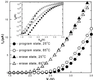
Fig. 1. MeasuredI –V curves for both linear and logarithmic scale, biased atV = 1:6 V, of two MXVANDcells in erase state and program state at room temperature and high temperature, respectively.
(CHE) injection at V. To emulate product operation, the drain bias steps from 3.0 to 4.4 V with V.
II. READCURRENTWINDOWNARROWING
Fig. 1 shows the – curves, biased at V, of MXVANDcells in erase state and program state at room tem-perature, and high temperature respectively. Here, the erase state and the program state represent the high bound of low- cells and the low bound of high- cells in 2-bits per cell product op-eration. If we read the data of cells at V, the read current window is about 8.77 A at room temperature. But the read cur-rent window reduces to 7 A when the cell operates at 85 C. The degraded read current window may cause an error during data sensing at high temperature especially when the other relia-bility issues [3], [4] are also taken into account. From the figure, it is found that the window narrowing mainly comes from the read current increment in program state.
When a MOSFET is operated at high temperature, two mech-anisms will affect the read current of device. One is the threshold voltage lowering, and the other is the mobility degradation [5], [6]. The former may increase the currents in subthreshold and weakly on regions. The later may degrade the currents in fully on region. As a result, there is usually a crossover between the current–voltage (I–V) curves of device measured at room tem-perature and high temtem-perature. In Fig. 1, the crossover behavior
496 IEEE ELECTRON DEVICE LETTERS, VOL. 25, NO. 7, JULY 2004
Fig. 2. Temperature effect(1I ) comparison between CHE programming and FN programming. The CHE programming is atV = 11 V, V steps from 3.0 to 4.4 with1V = 0:2 V, and the V steps from 17 to 19 V with 1V = 0:5 V for FN programming.
of the erase state cell happens at about V, and the cur-rent increment is insignificant in the weakly on region. But for the cell at program state, which has locally programmed charges at source side, the crossover behavior does not appear even when the applied is as high as 3.5 V. Because the impact of our 85 C measurement on trapped charge profile is confirmed in-significant (not shown), it is inferred that the localized distribu-tion of programmed charges enhance the subthreshold leakage current and results in a larger shift of – curve at high tem-perature. Thus, a delayed crossover point and a larger drain cur-rent increment are observed at the program state.
III. INFLUENCE OFTRAPPED-CHARGEPROFILE
In Fig.2, thecurrentincrements byusingCHEand FNprogram-ming are compared. is defined as the maximum read current differencebetweenroomtemperatureand85 C,and inFig.2 is the window. As programmed is increased, the read for extraction should also increase to keep the constant gate overdrive. The increases with increasing CHE programmed but it keeps almost the same for the cells by FN programming. This result suggests that the temperature effect on read current is enhanced by a localized charge profile and is worsened when the program/erase window is increased.
In the subthreshold region, the drain current is dominated by diffusion current [7] and can be expressed as
where is the maximum surface potential. Although the first term is a function of temperature, the current incre-ment at high temperature is dominated by the second term due to the exponential dependence. Therefore, the entirely different behavior between FN programming and CHE program-ming originates from the difference. The characteri-zation of in FN and CHE programmed cells will be discussed in the following.
IV. RELATIONSHIPBETWEENTRAPPEDCHARGEPROFILE AND
CURRENTINCREMENT
To characterize the observation of Fig. 2, a 2-D simulation [8], [9] is utilized to compare the surface potential of cells by
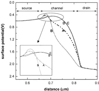
Fig. 3. Simulated surface potential distribution in cells with differentV by FN and CHE programming. (a) CHE,1V = 0:5 V at V = 1:5 V. (b) CHE, 1V = 2:0 V at V = 3:0 V. (c) FN, 1V = 0:5 V at V = 1:5 V. (d) FN,1V = 2:0 V at V = 3:0 V. The applied bias is V = 1:6 V with a constant gate overdrive.
Fig. 4. Relationship between temperature effect(1I ) and both charge density (H) and charge width (W). The charge density is modified with a fixed width 30 nm over channel, and the charge width is modified with a fixed density02 3 10 (1=cm ) over channel.
CHE programming and FN programming. Fig. 3 shows the sim-ulated surface potential distribution of cells with different by FN and CHE programming. One can see that the cells by FN programming have a constant due to the constant gate overdrive. As a result, similar is obtained in the FN pro-grammed cells. As to the CHE propro-grammed cells, the
are dominated by the local potential barrier, which is pulled high by the local trapped charge. Consequently, if the same are programmed by FN injection and CHE injection, the CHE pro-grammed cell would have a larger and much more se-rious temperature effect. In addition, is increased with increasing CHE programmed even the constant gate over-drive is adopted, as shown in Fig. 3. Thus, is increased with increasing CHE programmed .
LIU et al.: TEMPERATURE EFFECT ON READ CURRENT 497
To further clarify how the temperature effect is influenced by a localized charge profile, the relationship between and both the charge density and the charge width are characterized by simulation. As illustrated in Fig. 4, when the charge density is increased with a fixed width, the is increased due to the increased . In addition, when the charge distribu-tion is narrowed with a fixed density, the programmed be-comes smaller and only a smaller should be applied to ex-tract . It leads to a larger and the increased . As the charge width is narrower than a certain value,
would reduce substantially due to drain-induced barrier low-ering. Thus, the turns to decrease when the charge dis-tribution is narrower than a certain width.
V. CONCLUSION
In this work, the temperature effect of a two-bit ni-tride-storage Flash memory cell is investigated. A significant program-state read current increment in a CHE programmed cell is observed at high temperature. It degrades the read current window and impacts on data sensing. A localized charge profile that enhances the subthreshold leakage at high temperature may be the root cause of this current increment. From two-di-mensional simulation results, the current increment becomes larger as the charge density is higher or the charge distribution is narrower in a certain range.
REFERENCES
[1] B. Eitan, P. Pavan, I. Bloom, E. Aloni, A. Frommer, and D. Finzi, “NROM: A novel localized trapping, 2-bit nonvolatile memory cell,”
IEEE Electron Device Lett., vol. 21, pp. 543–545, Nov. 2000.
[2] M. K. Cho and D. M. Kim, “High performance SONOS memory cells free of drain turn-on and over-erase: compatibility issue with current Flash technology,” IEEE Electron Device Lett., vol. 21, pp. 399–401, Aug. 2000.
[3] W. J. Tsai, N. K. Zous, C. J. Liu, C. C. Liu, C. H. Chen, T. H. Wang, S. Pan, C. Y. Lu, and S. H. Gu, “Data retention behavior of a SONOS type two-bit storage Flash memory cell,” in IEDM Tech. Dig., pp. 32.6.1–32.6.4.
[4] C. C. Yeh, W. J. Tsai, T. C. Lu, S. K. Cho, T. Wang, S. Pan, and C.-Y. Lu, “A modified read scheme to improve read disturb and second bit effect in a scaled MXVAND Flash memory cell,” in Proc. Non-Volatile
Semiconductor Memory Workshop, 2003, pp. 44–45.
[5] F. S. Shoucair, “Design considerations in high temperature analog CMOS integrated circuits,” IEEE Trans. Comp., Hybrids, Manufact.
Technol., vol. CHMT-9, pp. 242–251, Sept. 1986.
[6] , “Scaling, subthreshold, and leakage current matching characteris-tics in high-temperature (25 C–250 C) VLSI CMOS devices,” IEEE
Trans. Comp., Hybrids, Manuf. Technol., vol. 12, pp. 780–788, Dec.
1989.
[7] T. A. Fjeldly, “Threshold voltage modeling and the subthreshold regime of operation of short-channel MOSFET’s,” IEEE Trans. Electron
De-vice, vol. 40, pp. 137–145, Jan. 1993.
[8] E. Lusky, Y. Shacham-Diamand, I. Bloom, and B. Eitan, “Character-ization of channel hot electron injection by the subthreshold slope of NROM device,” IEEE Electron Device Lett., vol. 22, pp. 556–558, Nov. 2001.
[9] E. Lusky, I. Bloom, and B. Eitan, “Investigation of the spatial distri-bution of CHE injection utilizing the subthreshold slope and the Gate induced drain leakage (GIDL) characteristics of the NROM device,” in