ELSEVIER Physica B 219&220 (1996) 65 67
Effect of phonon scattering on free-carrier absorption
in quantum well structures
C h h i - C h o n g W u a'*, C h a u - J y L i n b
"Institute of Electronics, National Chiao Tung University, Hsinchu, Taiwan bDepartment of Applied Mathematics, National Chiao Tung University, Hsinchu, Taiwan
Abstract
The free-carrier absorption has been studied for quantum well structures fabricated from III-V semiconductors such as n-type InSb films when the acoustic phonon scattering is dominant. The energy band of carriers in semiconductors is assumed to be nonparabolic. The scattering mechanisms of phonons with carriers in semiconductors are considered for the deformation-potential coupling and the piezoelectric coupling separately. Results show that the free-carrier absorp- tion coefficient in n-type InSb films depend upon the polarization of the radiation field relative to the direction normal to the quantum well structures, the photon frequency, the film thickness and the temperature. It is also found that the free-carrier absorption coefficient could be complex due to the interaction of the radiation field and the photon field with carriers in semiconductors. Thus, the index of refraction of semiconducting films could be changed due to this c a r r i e ~ p h o n o n - p h o t o n interaction.
1. Introduction 2. Theory
In a magnetic field where the carrier motion is con- fined to a plane perpendicular to the magnetic field, the free-carrier absorption coefficient ~ depends upon the photon polarization relative to the magnetifc field [1]. For carriers confined in a quasi-2D structure, it was found that ~ depends upon the polarization of the radi- ation field relative to the direction normal to the quasi- 2D structure [2]. For II! V compound semiconductors, the electron phonon interaction is dominated by the deformation-potential and piezoelectric couplings [3]. Thus, we investigate the effect of the acoustic phonon on in n-type InSb films with a quasi-2D structure. The energy band of electrons in semiconductors is assumed to be nonparabolic.
For a square well potential along the z-axis with infi- nitely high barriers at z = 0 and z = d, the electron field operator ~u(r) is given [4, 5] by
I//(1") =
n:lkE
~ b k . e x p ( i k ' x ) s i n ~ - ) , (1) where r = (x, z) = (x, y, z), V = dS is he film volume with the surface area S and the film thickness d, k = (kx, ky) is the electron wave vector, and bk, is the electron annihila- tion operator. The electron energy is given [3] by the relationER.'~ h2k 2 (r~hn) 2
Ek. 1 + E~.o) = 2m---¥ + 2m*d~' n = 1, 2, 3 ... (2)
* Corresponding author. where m* is the effective mass of electron.
0921-4526/96/$15.00 .i?' 1996 Elsevier Science B.V. All rights reserved SSDI 0 9 2 1 - 4 5 2 6 ( 9 5 ) 0 0 6 5 1 - 6
66
C.-C. Wu. C. Jy. Lin/Physica B 219&220 (1996) 65 67
The absorption coefficient for the absorption ofphotons can be expressed [-2] as
~ 1 / 2
e = ~oc~i Wif~,
(3)where e is the dielectric constant of material, no is the n u m b e r of photons in the radiation field, ,f~ is the distri- bution of carriers, and Wi is the transition probability. F r o m the Born a p p r o x i m a t i o n
W, = 2--~f [,(f,M+li)lZ 6(Ef - E, - hf2 - ho)q)
+ ](flM_li)123(Ef - E , - hf2
+hOgq)],
(4) where E~ andEf
are the initial and final electron energies, hf2 is the p h o t o n energy, and hcoq is the p h o n o n energy. F o r interaction between electrons, photons, and phonons, the transition matrix elements(flM+_ li)
are given by_
= ~'F. (flH,aalj)(jIVdi)
( f l M +li)
~ L
E j - Ei --T- h~q
( f [ VslJ) (jlnradl i) 1
where Hraa
is the electron-photon
interaction and Vs is the scattering potential due to the e l e c t r o n - p h o n o n inter- action. The e l e c t r o n - p h o t o n interaction is given byHra d --
5(27~hno/gf2V)l/Zg'p,
(6)is the p h o t o n polarization vector and p is the electron momentum. Its matrix elements for electrons in the same band are given as follows.
(i) When the p h o t o n is polarized parallel to the layer plane,
(k' n'lHradlkn) = -- e~(2rch3no/~QV)l/2
m*
X ~° k~)n,,n(~k~,,k~,
(~k',,k,"
(7a)(ii) When the p h o t o n is polarized perpendicular to the layer plane,
(k'n'lHr,dlkn) --
~-.d(2~h2no/~f2V)l-/2
{
1 -- cos{-rt(n' + n)] -~1 - c ° s [ ~ ( n ' - n ) ] } 6k~,k~'6kk"
X . . . . n ~ -I- n r ( - - n ~' (7b) The distribution function for a quasi-2D nondegener- ate electron gas can be expressed asfkn=(ned/2m*kBZ)l/2(~)Ii~latexp ( 2~8T/jEgal~
- 1Ega,
hZk 2 ]
x exp
2kBT
2m-~kBTJ'
(8)where ne is the concentration of electrons, and
a, = [-1 +
2(rthn)2/m*dZE'g] 1/2.
(9)There are two d o m i n a n t e l e c t r o n - p h o n o n interaction mechanisms in n-type InSb [-6]:
(i) F o r the deformation-potential coupling,
V s = (kBT/2pvZV) 1/2 E d
exp(iq, r), (10) where p is the density of material, vs is the sound velocity, q is the p h o n o n wave vector, and Ed is the deformation potential.(ii) F o r the piezoelectric coupling,
Vs = (kBT/2pv 2 V) 1/2 ([elflp/e[q[)
exp(iq "r), (11) where tip is the a p p r o p r i a t e piezoelectric constant.3. Numerical results
The relevant values of physical parameters for n-type InSb thin films are taken to be: ne = 1.75 x 1014 cm -3, m* = 0.013too (too is the free electron mass), p = 5.8 gm/ cm 3, e = 18, Eg -- 0.2 eV, Ed = 4.5 eV, tip = 1.8 × 10⁴ esu/ cm 2, and Vs = 4 x 105 cm/s.
In Fig. l(a), the free-carrier absorption coefficient
I~1
is plotted as a function of the p h o t o n frequency with d = 1 pm for the radiation field polarized parallel to the layer plane in th case of deformation-potential coupling. It shows thatI~1
decreases monotonically with increasing the p h o t o n frequency and increases with increasing tem- perature. In Fig. l(b), c~ is plotted as a function of the p h o t o n frequency with d = 1 pm for the radiation field10-3 -- 1 0 - 7 10-9 0
\\~Oo
....
°°°o~°.°.i''- .... Z.
'~-2/r ... i i i i 20 40 60 80 100 (THz) 10 6~o-7
10-8 10-9 1 0 - 1 1 0 '~x 300 K\i:%
• .. -,~ "~'/'r"".... "q I I I I " " 2O Z,0 60 80 100 f/(THz) Fig. 1. Free-carrier absorption coefficient for the deformation- potential coupling as a function of the photon frequency for photons polarized: (a) parallel to the layer plane and (b) perpen- dicular to the layer plane.C.-C. Wu, C. Jy. Lin/Physica B 219&220 (1996) 65 67 67 ~104
i
10-3 ~i0-5 10-7 103 "-.. ~" ,'% 7 ~"~-, "44'"'".... ' 5'17 25 75 lOO 2 ('rHz) 10 5' .,Z-..
(b)
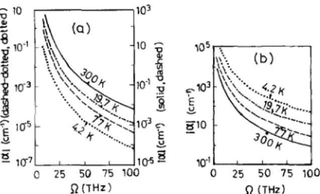
I 104 215 50 7L5 lO0 (THz)Moreover, the index of refraction of semiconducting films could be changed due to the c a r r i e r ~ h o n o n p h o t o n interaction. In Fig. 2(a), ]el is plotted as a function of the p h o t o n frequency with d = 1 gm for the radiation field polarized parallel to the layer plane in the case of piezoelectric coupling. It shows that lel decreases mono- tonically with increasing the p h o t o n frequency and in- creases with increasing temperature. While for the radi- ation field polarized perpendicular to the layer plane as shown in Fig. 2(b), it can be seen that
I~l
decreases monotonically with increasing the p h o t o n frequency, but J:~l decreases with increasing temperature.Fig. 2. Free-carrier absorption coefficient for the piezoelectric coupling as a function of the photon frequency for photons polarized (a) parallel to the layer plane and (b) perpendicular to the layer plane.
polarized perpendicular to the layer plane. It can be seen that the changing of c~ with temperature appears irregu- larly in lower frequencies with ~ < 25 THz. Since Im(~) is quite small c o m p a r e d to Re(e), thus ~ ~ lel in this case and e decreases with increasing the p h o t o n frequency.
R e f e r e n c e s
[1] T.M. Rynne and H.N. Spector, J. Appl. Phys. 52 (1981) 393. [2] H.N. Spector, Phys. Rev. B 28 (1983) 971.
[3] C.C. Wu, Phys. Rev. B 28 (1983) 7094.
[4] S. Tamura and T. Sakuma, Phys. Rev. B 16 (1977) 3936. [5] G. Bastard, J.A. Brum and R. Ferreira, Solid State Physics,
Vol. 44 (Academic Press, New York, 1991) p. 229. [6] B.R. Nag, Theory of Electrical Transport in Semiconduc-