Interfacial operator approach to computing band structures for photonic crystals
of polar materials
Ruey-Lin Chern,1,*Chien C. Chang,1,2,†and C. Chung Chang2
1Institute of Applied Mechanics, National Taiwan University, Taipei 106, Taiwan, Republic of China
2Division of Mechanics, Research Center for Applied Sciences, Academia Sinica, Taipei 115, Taiwan, Republic of China
共Received 24 January 2006; revised manuscript received 20 April 2006; published 27 June 2006兲 In this study, we propose an interfacial operator approach to compute surface phonon modes for one- and two-dimensional periodic arrays of polar materials in a finite-difference formulation. The key aspect of the approach is to introduce an interfacial variable along the interface between the polar material and the surround-ing dielectric material, which represents the local strength of the surface phonon modes along the interface. In this approach, the apparently nonlinear eigenvalue problem can be reformulated as a quadratic eigensystem, and thus further reduced to a standard linear eigenvalue problem. Band structures can be computed directly without the need of examining transmission spectra as in the finite-difference time-domain method, or locating the mode frequency by testing an auxiliary function in other methods. Applying the method to four different types of photonic crystals of polar materials, we are able to uncover several interesting results by studying the effect of dimension, the size共filling ratio兲 effect, the effects of the transverse optical phonon frequency 共T兲, and longitudinal optical phonon frequency共L兲 as well as the effect of shape or geometry of the polar material. DOI:10.1103/PhysRevB.73.235123 PACS number共s兲: 78.20.Bh, 42.70.Qs, 02.70.⫺c, 02.70.Bf
I. INTRODUCTION
Photonic crystals made of dielectric materials have been extensively studied since 1987.1,2 The most distinguished
feature is their full band gaps, where periodicity of the struc-ture provides a scattering mechanism to prohibit propagation of the electromagnetic field from all directions over certain ranges of frequencies. If the dielectrics are replaced by per-fect metals,3–9, the fields are completely expelled from the
metals and vanish inside. As a result, large band gaps can be opened up. If more realistic dispersive metals replace perfect conductors in the photonic structures,10–15collective motion
of free electrons gives rise to resonance in optical properties. In particular, surface plasmon modes may appear in the op-tical frequency range, and therefore, these structures are also named plasmonic crystals.16,17 On the other hand, if polar
materials replace the metals,18–21surface phonon modes may
result from the coupling of lattice vibration of the ionic structure and the electromagnetic field. In the meanwhile, densely distributed resonant cavity modes as well as other modes also arise in these structures. This type of periodic structures are termed as photonic crystals of polar materials or simply polaritonic crystals.21
The model for polar materials considered in the present study is given by22 共兲 = ⬁
冉
2−L 2 2− T 2冊
, 共1兲where⬁=共⬁兲 is the dielectric constant at a very high fre-quency,Tis transverse optical共TO兲 phonon frequency, and Lis the longitudinal optical共LO兲 phonon frequency, which is related toTthrough the Lyddane-Sachs-Teller 共LST兲 re-lation L
2
/T
2
=共0兲/共⬁兲. It is known that a polar material does not support propagating modes with frequencies inside the polariton gap共T⬍⬍L兲, while the bulk modes with frequencies outside the gap follow an anticrossing scheme. The situation changes drastically if we consider interfaces
between polar materials and other dielectrics. The simplest interface is a plane between the polar material and a sur-rounding dielectric. In this case, there exists the surface pho-non mode with the frequency inside the polariton gap. Letd be the dielectric constant of the surrounding medium. At the large wave number limit, the frequency of the surface pho-non mode approaches
sph=
冑
⬁L 2 +dT 2 ⬁+d , 共2兲which is called the surface phonon frequency. Furthermore, a periodic array of polar materials may fold the bands within the first Brillouin zone and produce extra bands not observed in a simple interface.
There is a large difference between the dielectric photonic crystals and those made of metals. For dielectrics, the elec-tric field produces a polarization in the same direction, and the band structures are scale invariant. For dispersive metals, the electric field produces an adverse polarization which may result in a negative dielectric constant due to the electron motion at frequencies below the plasma frequencyp. The band structures are no longer scale invariant because of the characteristicp of the metal. For arrays of polar materials, oscillation of the effective charges of the ions due to lattice vibration results in two distinct classes of resonant modes. One class of modes are analogous to the case of surface plasmons in dispersive metals, but usually occurs in the in-frared frequency range. These waves are surface phonons or surface phonon modes. The other are resonant cavity modes or waveguide modes corresponding to very large dielectric constants lying immediately belowT.
It has been difficult to compute eigenmodes and band structures of frequency-dependent materials, in particular, for transverse electric共TE兲 modes. The major difficulty comes from the apparently nonlinear formulation of the eigenvalue problem.23 Several approaches have been proposed to study
this problem, including plane wave expansion method20and
vectorial eigenmode expansion method.21 Other approaches such as transfer matrix method,18
layer-Korringa-Kohn-Rostoker method,24 multiple multipole method,15and
finite-difference time-domain method14 can also be applied to
frequency-dependent problems. Another difficulty comes from the special physical features of the solution. Localized surface plasmons for arrays of dispersive metal, as well as surface phonons for arrays of polar material, require very fine resolution schemes. An even more critical situation is that the dielectric function changes sign across the dielectric-metal or dielectric-polar material interface over some fre-quency ranges. This will cause the change of type of the eigensystem and may induce numerical instability in solving the eigenvalue problem.
In one of our previous papers,25we developed an interfa-cial operator approach to compute band structures for photo-nic crystals of dispersive metals. In particular, we considered the free-electron and the Drude models for the metal prop-erty. In this approach, the apparently nonlinear eigenvalue problem can be reformulated as a linear eigensystem which is solved by standard eigenvalue solvers. In the present study, we extend this approach to be applicable to photonic crystals of polar materials with the dielectric function in Eq. 共1兲. In this approach, we will obtain a quadratic eigensystem, which in turn can be reduced to a linear eigensystem at the expense of doubling the matrix size. Moreover, we can dis-pense with the need of examining transmission spectra as in the finite-difference time-domain method, or locating the mode frequency by testing an auxiliary function in other methods.
In the present study, we investigate the four types of po-laritonic crystals in Figs. 1共a兲–1共d兲. Special emphases are placed upon the frequency bands within the polariton gap in
addition to the resonant cavity modes with frequencies lying immediately belowT. The four different photonic crystals of polar materials enable examination of 共i兲 the effect of dimension between Fig. 1共a兲 and Figs. 1共b兲–1共d兲, 共ii兲 the size effect or the filling ratio effect共t/a, w/a, r/a兲, 共iii兲 the effect of the intrinsic frequencies T and L, as well as 共iv兲 the geometric effect 共different shapes of polar materials兲 be-tween Figs. 1共b兲–1共d兲. It would be helpful to summarize the main results here and refer to the following sections for more details.
共1兲 About the effect of dimension, it will be shown that while there are only two branches of surface phonon modes for one-dimensional arrays, our numerical results indicate that there is infinite number of surface phonon modes for two-dimensional crystals. However, resonant cavity modes are supported by polaritonic crystals in both dimensions.
共2兲 Regarding the effect ofTandL, it is of interest to see what would happen if we letTgo to zero andLtend to infinity. AsTgoes to zero, the resonant cavity modes dis-appear all together, and as L goes to infinity the surface phonon modes cannot be found with finite frequencies. It is further argued according to the Rayleigh quotient that the frequency bands of the polaritonic crystal will converge up-ward to those of the same photonic crystal made of perfect conductors. For finite values of L, there are other modes existing within the polariton gap in addition to the surface phonon modes. The transition of one such typical mode as Lgoes from finite values to infinity will be discussed.
共3兲 Concerning the size effect, it will be shown that if the filling ratio is large, the distribution of resonant cavity modes is more spread in frequency, and the bulk modes inside the polariton gap would be expelled more effectively out of the gap. On the other hand, if the thickness ratio becomes smaller, the bands of surface phonon modes aroundsphis broadening. It is also argued that anticrossing of band disper-sion of resonant cavity modes is also a size effect as the cutoff frequencies for TM modes are dependent upon the filling ratio.
共4兲 Finally with the effect of shape and geometry, it will be shown that the bands of TE modes for the array of circular cylinders could completely fill in the polariton gap and does not allow full photonic band gap within it, while the bands of TE modes for the array of grid cylinders are relatively more flat, and thus allowing full photonic band gaps within the polariton gap. It is also shown and argued that the arrays of grid cylinders are more effective in lifting the degeneracy of surface phonon modes than the arrays of circular cylinders.
II. INTERFACIAL OPERATOR APPROACH
The time-harmonic wave equations for linear, isotropic and nonmagnetic materials in two dimensions are given by
−1 ⵜ2E =
冉
c冊
2 E, 共3兲 − ·冉
1 H冊
=冉
c冊
2 H 共4兲for TM and TE modes, respectively. For periodic structures, it is sufficient to solve the problem on one unit cell along FIG. 1. 共Color online兲 Plasmonic crystals made of dispersive
metals.共a兲 1D layered structure, 共b兲 2D array of square cylinders, 共c兲 2D array of circular cylinders, and 共d兲 2D array of grid cylinders.
with Bloch’s condition as the boundary condition
E共r + ai兲 = eik·aiE共r兲, 共5兲
H共r + ai兲 = eik·aiH共r兲, 共6兲
where k is the wave vector and ai 共i=1,2兲 are the lattice translation vectors. For frequency-dependent materials, the eigensystem no longer has a standard format since the eigen-value itself appears in the solution operator
L共⌳兲=⌳, 共7兲
where⌳=2/ c2 is the eigenvalue, and is the eigenfunc-tion, which can be either the E or the H field. If we discretize Eq.共7兲 in a straightforward manner, for example, by a finite-difference scheme, we will obtain a nonlinear eigensystem
A共⌳兲x = ⌳x, 共8兲
where A is the matrix system and x is the eigenvector. This is one type of nonlinear eigenvalue problem, that is, nonlinear in eigenfrequency. However, if the dielectric function of the material has an analytical form, we are able to reformulate the original nonlinear eigenvalue problem as a standard eigensystem. For example, the eigensystem for TM modes 共3兲, applied with the dielectric function 共1兲, can be written as
−ⵜ2E =⬁
冉
⌳ − ⌳L⌳ − ⌳T
冊
⌳E 共9兲or, rearranged in the following form:
冋
⌳2−⌳冉
⌳L− 1⬁ⵜ2
冊
− ⌳T⬁ⵜ2
册
E = 0, 共10兲 which is a quadratic eigensystem, with ⌳T=T2/ c2 and ⌳L =L2
/ c2. By introducing an auxiliary variable E
⬘
=⌳E, Eq. 共10兲 can be written as冤
0 I ⌳T ⬁ⵜ 2 ⌳L− 1 ⬁ⵜ 2冥
冋
E E⬘
册
=⌳冋
E E⬘
册
. 共11兲This is a linear eigensystem with standard format, which can be solved by standard eigenvalue solvers at the expense of doubling the matrix size. However, this could not be done for the TE modes 共4兲, for the dielectric function lies inside the operator.
In our previous study25 we have proposed the interfacial
operator approach to compute surface plasmon modes for periodic structures made of dispersive metal, based on the free-electron model. Here, we extend this approach to be applicable to polar materials.
The basic idea is first to deal with the eigensystem共4兲 in the strict insides of the dielectric and the polar material sepa-rately, so that the dielectric function can be moved out of the operator in either region as follows:
− 1
dⵜ2H =⌳H, 共12兲
−ⵜ2H =⬁
冉
⌳ − ⌳L⌳ − ⌳T
冊
⌳H, 共13兲whered is the dielectric constant of the dielectric material. In the polar material, Eq. 共13兲 is further rearranged in the same manner of Eq.共10兲 as
冋
⌳2−⌳冉
⌳L− 1⬁ⵜ 2
冊
− ⌳T⬁ⵜ
2
册
H = 0. 共14兲Next, consider discretization of Eqs. 共12兲 and 共14兲 in a one-dimensional lattice with the ith point at the interface. The dielectric medium lies to the left of the ith point, the polar material to the right. If we discretize Eqs.共12兲 and 共14兲 in the strict insides of the dielectric medium and the polar material, respectively, we obtain a system of equation of the form
A共n−1兲⫻n共⌳兲Hn= 0, 共15兲
where A is an共n−1兲⫻n matrix, and is quadratic in ⌳, Hnis the column vector of all discrete H fields, and Hn−1 =关H1, . . . , Hi−1, Hi+1, . . . , Hn兴Tis a subset of H
nexcluding Hi at the interface. It is obvious that Eq.共15兲 does not constitute an eigenvalue problem because the matrix A is not square. One more equation is needed. In fact, Eqs.共12兲 and 共14兲 are connected by an interface condition
冋
1 H
n
册
S= 0, 共16兲
where/n denotes the derivative in the surface normal
di-rection, and 关¯兴S denotes the jump across the interface S. The interface condition共16兲 is obtained by integrating both sides of the eigensystem共4兲 over a thin box located on the interface, and taking the limit as the box height goes to zero. Applying the dielectric function 共1兲 for the polar material, the interface condition共16兲 becomes
1 d
冏
H n冏
+ = 1 ⬁冉
⌳ − ⌳T ⌳ − ⌳L冊
冏
H n冏
− , 共17兲where + and − denote the dielectric and the polar material regions, respectively. The next step is to rearrange Eq.共17兲 as follows: ⌳L d
冏
H n冏
+− ⌳T ⬁冏
H n冏
−=⌳S, 共18兲so that the eigenvalue⌳ only appears on the right-hand side, where S⬅ 1 d
冏
H n冏
+−冏
1 ⬁ H n冏
− 共19兲is a weighted difference of the normal derivatives of the H field across the interface.
Apparently, Eqs.共12兲 and 共14兲, supplemented by Eq. 共18兲, cannot be formulated as a standard eigensystem in terms of
H, for the right-hand side of Eq.共18兲 contains the derivatives
of H. This difficulty can be removed by considering a finite-difference formulation. Recall that Eqs. 共12兲 and 共14兲 have been put in the discretized form, Eq.共15兲. We will also
dis-cretize Eq.共18兲 at the interface point i to yield −⌳L dHi−1+
冉
⌳L d + ⌳T ⬁冊
Hi− ⌳T ⬁Hi+1=⌳
冉
−⬁Hi−1+sumHi−dHi+1d⬁
冊
, 共20兲wheresum=⬁+d. The advantage of discretizing Eq.共18兲 is now clear that the right-hand side of Eq.共20兲 is simply linear combination of the discrete variables Hi−1, Hi, and Hi+1. The next key step is to introduce an interfacial variable
Ri⬅
−⬁Hi−1+sumHi−dHi+1
d⬁ 共21兲
to replace Hiat the interface. Equivalently,
Hi=
⬁Hi−1+d⬁Ri+dHi+1 sum
. 共22兲
Let⌳1=⌳L−⌳Tand⌳2=⬁⌳L+d⌳T. Substituting Eq.共22兲
for Hiin Eq.共20兲 yields 1
sum
共− ⌳1Hi−1+⌳2Ri+⌳1Hi+1兲 = ⌳Ri, 共23兲
which makes the interface variable Rian ideal substitute for
Hi in formulating the eigenvalue problem. Moreover, we note that Riis a discrete version of S in Eq.共19兲, and thus a measure of the weighted difference of the normal derivative H /n in two sides of the interface. This important property
enables Ri to represent the local strength of surface phonon modes at the interface as a surface phonon mode decays rapidly from the interface into both the polar material and the surrounding dielectric.
Finally, all Hi appearing in Eq. 共15兲 is replaced by the right-hand side of Eq.共22兲. Then, Eq. 共15兲 supplemented by Eq. 共23兲 now constitutes a standard quadratic eigenvalue problem of the form
An⫻n共⌳兲H˜n= 0, 共24兲 where An⫻nis a square matrix, and is quadratic in⌳, and H˜n is Hnwith Hireplaced by Ri. Alternatively, Eq. 共24兲 can be recast into a more explicit form
共⌳2−⌳B − C兲H˜ = 0, 共25兲
where H˜ =H˜n, B and C are square matrices. Equation 共25兲 can be written as a linear eigensystem of double size as fol-lows:
冋
0 I C B册
冋
H˜ H˜⬘
册
=⌳冋
H ˜ H˜⬘
册
, 共26兲where H˜
⬘
=⌳H˜ . In the discrete sense, the eigensystem 共26兲 has the same eigenvalue as the original eigensystem共8兲, al-though the eigenvector H˜ is slightly different from the origi-nal eigenvector H. However, they can be converted back and forth between each other through Eqs.共21兲 and 共22兲. Most importantly, Eq.共26兲 is a standard eigenvalue problem, and can be solved by many eigenvalue solvers.The above formulation can be applied to any number of interfaces. One only needs to introduce the same number of interfacial variables.
III. EXTENSION TO TWO DIMENSIONS
The method formulated above can be extended to two dimensions in a straightforward manner. However, the details are much more involved than in the one-dimensional 共1D兲 case.
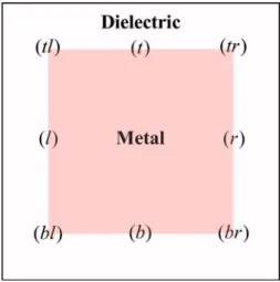
First of all, we discretize the Eqs. 共12兲 and 共14兲 in the strict insides of the dielectric and the polar material by a central finite-difference scheme, respectively. The resulting matrix system is then supplemented by introducing the inter-facial variables at the interface between the two media. Fig-ure 2 shows a schematic diagram for the interfacial operator approach in a two-dimensional structure. There are eight types of interface points in 2D. Four types of them appear at sides: left, right, bottom, and top, which are denoted by共l兲, 共r兲, 共b兲, and 共t兲, respectively, and the other four types appear at corners: bottom left, bottom right, top left and top right, which are denoted by 共bl兲, 共br兲, 共tl兲, and 共tr兲, respectively. This is due to four different surface normal directions in 2D: vertical, horizontal, and two diagonals, compared to only one direction in 1D. As a result, there are eight types of interfa-cial variables in 2D defined as follows:
Ri,j共l兲⬅−⬁Hi−1,j+sumHi,j−dHi+1,j
d⬁ ,
Ri,j共r兲⬅−dHi−1,j+sumHi,j−⬁Hi+1,j
d⬁ ,
Ri,j共b兲⬅−⬁Hi,j−1+sumHi,j−dHi,j+1
d⬁ ,
Ri,j共t兲⬅−dHi,j−1+sumHi,j−⬁Hi,j+1
d⬁ ,
FIG. 2. 共Color online兲 A schematic diagram for the interfacial operator approach in a two-dimensional structure.
Ri,j共bl兲⬅ −⬁Hi−1,j−1+sumHi,j−dHi+1,j+1
d⬁ ,
Ri,j共br兲⬅−⬁Hi+1,j−1+sumHi,j−dHi−1,j+1
d⬁ ,
Ri,j共tl兲⬅−dHi+1,j−1+sumHi,j−⬁Hi−1,j+1
d⬁
,
Ri,j共tr兲⬅−dHi−1,j−1+sumHi,j−⬁Hi+1,j+1
d⬁ 共27兲
or, equivalently,
Hi,j=
⬁Hi−1,j+d⬁Ri,j共l兲+dHi+1,j sum
,
Hi,j=
dHi−1,j+d⬁Ri,j共r兲+⬁Hi+1,j sum
,
Hi,j= ⬁Hi,j−1+d⬁Ri,j
共b兲+dH
i,j+1 sum
,
Hi,j=
dHi,j−1+d⬁Ri,j共t兲+⬁Hi,j+1
sum
,
Hi,j=
⬁Hi−1,j−1+d⬁Ri,j共bl兲+dHi+1,j+1 sum
,
Hi,j=⬁Hi+1,j−1+d⬁Ri,j
共br兲+dH
i−1,j+1 sum
,
Hi,j=
dHi+1,j−1+d⬁Ri,j共tl兲+⬁Hi−1,j+1
sum
,
Hi,j=
dHi−1,j−1+d⬁Ri,j共tr兲+⬁Hi+1,j+1 sum
. 共28兲
Following the same procedure for Eq.共23兲 in 1D, eight in-terface conditions in 2D can be formulated as
1 sum
共− ⌳1Hi−1,j+⌳2R共l兲i,j+⌳1Hi+1,j兲 = ⌳Ri,j共l兲,
1 sum
共⌳1Hi−1,j+⌳2R共r兲i,j −⌳1Hi+1,j兲 = ⌳Ri,j共r兲,
1 sum
共− ⌳1Hi,j−1+⌳2R共b兲i,j +⌳1Hi,j+1兲 = ⌳Ri,j共b兲,
1 sum
共⌳1Hi,j−1+⌳2Ri,j共t兲−⌳1Hi,j+1兲 = ⌳Ri,j共t兲,
1 sum
共− ⌳1Hi−1,j−1+⌳2R共bl兲i,j +⌳1Hi+1,j+1兲 = ⌳Ri,j共bl兲,
1 sum
共− ⌳1Hi+1,j−1+⌳2R共br兲i,j +⌳1Hi−1,j+1兲 = ⌳Ri,j共br兲,
1 sum
共⌳1Hi+1,j−1+⌳2R共tl兲i,j −⌳1Hi−1,j+1兲 = ⌳Ri,j共tl兲,
1 sum
共⌳1Hi−1,j−1+⌳2R共tr兲i,j −⌳1Hi+1,j+1兲 = ⌳Ri,j共tr兲. 共29兲
As to the strict insides of the dielectric and the polar mate-rial, Eqs.共12兲 and 共14兲 are discretized to give
⌳2H i,j+⌳
冉
1 dh2Li,j冊
= 0, 共30兲 ⌳2H i,j+⌳冉
1 ⬁h2Li,j−⌳LHi,j冊
− ⌳T ⬁h2Li,j= 0, 共31兲where Li,j= Hi−1,j+ Hi,j−1− 4Hi,j+ Hi+1,j+ Hi,j+1.
Second, since there are four neighbor points instead of two, incorporated in the discretization of theⵜ2 operator in
2D, replacing Hi,j at the interface in Eqs.共30兲 and 共31兲 with
Rijthrough Eq.共28兲 becomes more complicated in 2D. How-ever, this could be done in a systematic and efficient way. Equations共29兲 to 共31兲 are combined together to form a qua-dratic eigensystem in the same form of Eq. 共25兲, which in turn can be written as a linear eigensystem as in Eq.共26兲.
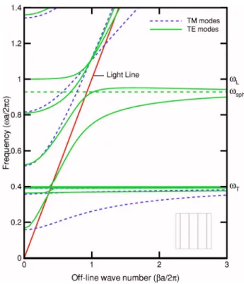
FIG. 3. 共Color online兲 The dispersion relations at k=0 for a one-dimensional polaritonic layered structure关Fig. 1共a兲兴 of thick-ness t / a = 0.2, whereTa / 2c=0.4, La / 2c=1, and ⬁= 5.1.
IV. RESULTS AND DISCUSSION
In the present study, we consider the polar material TlCl used in Ref. 21, where ⬁⫽5.1, Ta / 2c⫽0.4, and La / 2c⫽1.0 for the lattice constant a=10m. Ford⫽1, we havespha / 2c⫽0.9286, according to Eq. 共2兲. First of all, we will study the one-dimensional crystal in Fig. 1共a兲, and then proceed with the study of two dimensional crystals in Figs. 1共b兲–1共d兲.
A. 1D array of polar materials
For the one-dimensional layered structures 关Fig. 1共a兲兴, there are two surface phonon modes inside the polariton gap 共T⬍⬍L兲 for the TE bands. One has a lower frequency with odd symmetry and the other has a higher frequency with even symmetry. Figure 3 shows the dispersion relations at the zone center共k=0兲 for the thickness ratio t/a=0.2. The insets show the eigenmodes of two TE bands at the off-line wave numbera / 2= 2, and of the lower band at a / 2
= 0.7, where is the wave number parallel to the interface. Note that a crossing scheme is observed between the two TE bands in the polariton gap for k = 0. Near the crossing point, usually at a small off-line wave number, the mode of the lower TE band switches from even symmetry to odd symme-try. In addition, we see an anticrossing scheme between the two TE bands inside the polariton gap for k⫽0. Figure 4 shows the dispersion relations at ka / 2= 0.1 for the same structure in Fig. 3. In this case, the eigenmodes of the two TE bands no longer possess perfectly different symmetries of odd and even at small off-line wave numbers. This is due to
the phase difference eikaof the modes between the two sides of the unit cell, as can be seen from the Bloch condition共6兲. In view of the similar symmetries of the modes, no intersec-tions can be found between the two TE bands.26 However,
they eventually grow into even and odd modes at large off-line wave numbers, for the fields at the unit cell boundary become very small due to the evanescent nature of surface phonon modes.
Splitting of the modes comes from interaction of surface phonons on both sides of the polar material as well as the dielectric. The mode with even symmetry has a higher fre-quency because the mode structure has a larger area that effectively corresponds to a larger energy. At sufficiently large off-line wave numbers, the frequencies of two surface phonon modes converge to the same frequencysphgiven in Eq. 共2兲. For a very thin structure, convergence of surface phonon modes is slow. This is due to effective interaction of the modes from both sides of the polar material, which lifts the degeneracy. Figure 5 shows the dispersion relations at
ka / 2= 0.5 for the thickness ratio t / a = 0.1. In a range of medium fractions of the polar material, convergence of sur-face phonon modes becomes faster. However, for a very high filling fraction, convergence is slow again, for the degen-eracy is again lifted by effective interaction of the modes from both sides of the dielectric. Figure 6 shows the disper-sion relations at the zone edge共ka/2= 0.5兲 for the thickness ratio t / a = 0.9. In the meanwhile, the higher TE band inside the polariton gap has a higher frequency that approaches the LO phonon frequencyLat zero off-line wave number. This is reasonable for the whole lattice is almost filled with the polar material. Another important fact in Fig. 6 is the nega-FIG. 4. 共Color online兲 The dispersion relations at ka/2=0.1
for a one-dimensional polaritonic layered structure 关Fig. 1共a兲兴 of thickness t / a = 0.2, where Ta / 2c=0.4, La / 2c=1, and ⬁ = 5.1.
FIG. 5. 共Color online兲 The dispersion relations at ka/2=0.5 for a one-dimensional polaritonic layered structure 关Fig. 1共a兲兴 of thickness t / a = 0.1, where Ta / 2c=0.4, La / 2c=1, and ⬁ = 5.1.
tive group velocity of the higher TE band, which occurs as the dielectric portion becomes sufficiently small. This is con-sistent with the property of left handedness for the wave-guide stack in Ref. 27, which serves as an approach to mak-ing a material with a negative index of refraction. Figure 6 also shows that as the thickness ratio t / a is close to 1, all the frequency bands共bulk modes兲 are expelled from the polar-iton gap, except the two TE bands 共surface modes兲 which converge tosphfrom below and above, respectively, at large off-line wave numbers.
In addition to surface phonon modes inside the polariton gap, a large number of nearly dispersionless bands for both TM and TE modes intensively gather around the TO phonon frequency T from below. They are resonant cavities modes28which correspond to very large values of dielectric
constant. Figure 6 further shows that the bands of resonant cavity modes are more spread if the thickness ratio t / a is large. This can be explained by examining the waveguide modes in high- cylinders, and we will come back to this point in the discussion for two-dimensional arrays of polar materials.
B. 2D arrays of polar materials
In order to ensure the accuracy of the eigenfrequencies, computations are performed on five different grids. Table I lists the numerics of2 and48 for TE modes at the zone
center⌫ for a square array of square cylinders in Fig. 1共b兲. Here,2 is the first nonzero eigenfrequency, and48 is the
48th eigenfrequency which is close to the TO phonon fre-quencyT. The computed results show good agreements
be-tween different grid resolutions. Figure 7 also shows the dis-tribution of eigenfrequencies for the same structure. The frequencies are little dependent on the grid level except in two distinct regions: one below the TO phonon frequencyT 共resonant cavity modes兲 and one around the surface phonon frequency sph 共surface phonon modes兲. As expected, the
modes intensively distributed belowTare the resonant cav-ity modes, which we have also observed in one-dimensional layered structures. However, contrary to the one-dimensional polaritonic crystals which have only two branches of surface phonon modes, the two-dimensional polaritonic crystals ap-parently have infinite degrees of surface phonon mode gath-ering around the surface phonon frequency sph. The same figure appears to indicate that the number of resolved surface phonon modes 共resonant cavity modes兲 increases linearly 共quadratically兲 with the number of grid points.
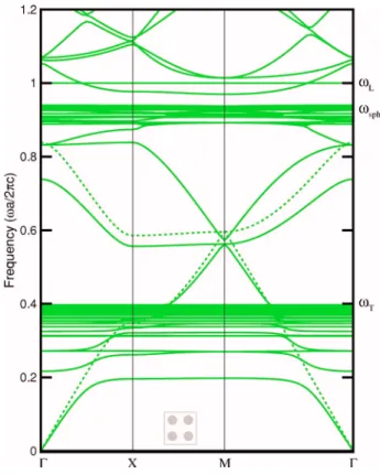
In order to see the fuller details, we plot the bands of TM and TE modes separately in Figs. 8 and 9 for a square array of circular cylinders of radius r / a = 0.3 in Fig. 1共c兲. The same figures also show the bands of the metallodielectric crystal for comparison, where polar materials are replaced by per-fect conductors. Both polarizations共TM and TE兲 have reso-nant cavity modes. However, only one polarization共TE兲 has surface phonon modes. These two types of modes 共surface phonon modes and resonant cavity modes兲 come from differ-ent physical origins. For frequencies immediately belowT, there is large dielectric constant which can support infinite degrees of resonant cavity modes. On the other hand, surface phonon modes come from the coupling between the electro-magnetic wave and vibration of the ionic charge of the polar FIG. 6. 共Color online兲 The dispersion relations at ka/2=0.5
for a one-dimensional polaritonic layered structure 关Fig. 1共a兲兴 of thickness t / a = 0.9, where Ta / 2c=0.4, La / 2c=1, and ⬁ = 5.1.
TABLE I. Convergence test for the eigenfrequency against the grid size.
Ngrid 202 302 402 502
2a / 2c 0.2580 0.2583 0.2585 0.2585
48a / 2c 0.3887 0.3895 0.3906 0.3911
FIG. 7.共Color online兲 The eigenfrequencies for TE modes ver-sus the index of eigenmode computed with different grid resolutions at the point⌫ for a square array of square cylinders 关Fig. 1共b兲兴 of half width w / a = 0.2 where Ta / 2c=0.4, La / 2c=1, and ⬁= 5.1.
material, which is not allowed for TM modes.
If T goes down to zero, resonant cavity modes would disappear, andLwould act similar top共plasma frequency in the free-electron model for dispersive metals兲. If also L goes to infinity, the frequency of surface phonon modes would go to infinity as well, and all the other bands would converge upward to the bands of the metallodielectric crys-tals. This upward convergence can be explained by consid-ering the Rayleigh quotient for TE modes 共also for TM modes兲 RH= 具H,LH典 具H,H典 , 共32兲 where具f ,g典=兰V cellf
*gddenotes the inner product of f and g
over the unit cell Vcell. Each eigenfrequency is obtained by minimizing the Rayleigh quotient with respect to functions which are orthogonal to all the lower frequency modes. Note that perfect conductors expel fields completely. The metall-odielectric crystal therefore has less freedom in distributing the energy in the unit cell, and has higher eigenfrequencies compared to the arrays of polar materials which allow lim-ited energy distribution in themselves. Below, we shall focus on discussion of resonant cavity modes and surface phonon modes separately.
1. Resonant cavity modes
Important physics related to resonant cavity modes have been investigated in depth in Ref. 28, such as anticrossing
interaction of the TE bands with the metallodielectric bands, node switching from one pattern to another, flux expulsion with small changes in frequency across the TO phonon fre-quency T, and so forth. Although resonant cavity modes have similar dispersionless characteristic as surface phonon modes, they are bulk modes in nature, and the number of which is even larger than that of surface phonon modes. From Fig. 7, we see that the number of stationary modes around the TO phonon frequencyTincreases quadratically with the grid resolution. This is consistent with the reso-nances of the square cavity to the metallic waveguide modes with frequencies lm determined by two free indices l and
m28
lm= c
2w
冑
lm冑
l2+ m2, 共33兲
wherelm=⬁共lm2 −2L兲/共lm2 −T2兲. Solving Eq. 共33兲 forlm yields28 lm 2 = 2⍀lm 2 T 2 L 2 +⍀lm2 +
冑
共L 2 +⍀lm2 兲2− 4⍀lm2 T 2, 共34兲where⍀lm=c
冑
l2+ m2/ 2w冑
⑀⬁with w the half width of the square cavity. The expression共34兲 indicatesTis the upper limit frequency of resonant cavity modes for if⍀lm goes to infinity,lmapproachesT. On the other hand, if⍀lmgoes to 0,lmapproaches⍀lmT/L. Therefore, for large fraction of FIG. 8.共Color online兲 The TM band structure for a square arrayof circular cylinders 关Fig. 1共c兲兴 of radius r/a=0.3, where Ta / 2c=0.4, La / 2c=1, and ⬁= 5.1. The dashed lines denote the bands of metallodielectric crystals obtained by replacing the polar material with a perfect metal.
FIG. 9. 共Color online兲 The TE band structure for a square array of circular cylinders 关Fig. 1共c兲兴 of radius r/a=0.3 where Ta / 2c=0.4, La / 2c=1, and ⬁= 5.1. The dashed lines denote the bands of metallodielectric crystals obtained by replacing the polar material with a perfect metal.
polar materials, that is, large value of w / a, the resonant bands spread more widely.
As the frequency approaches T from below, the bands become more concentrated. All these bands are flattened ex-cept an anticrossing interaction with the bands of metallodi-electric crystals共by replacing the polar material with a per-fect metal兲, in particular, for TE modes. The anticrossing interaction is present only for modes with even symmetry with respect to the wave vector, and is possible due to small but finite leakage of the modes out of the polar material,28
while the field for the metallodielectric structure is com-pletely compelled from the perfect metal. In Fig. 10, we plot the portion of the TE bands along the⌫-X path for a square array of square cylinders of half width w / a = 0.2, along with the real part of the magnetic field of the eigenmodes for the second polaritonic band and the first metallodielectric band at ka / 2= 0.4, which is near the anticrossing point. We can observe the leakage of the magnetic field out of the polar material in Fig. 10共b兲, with a contrast to the completely ex-pelled field out of the perfect metal in Fig. 10共c兲. The overlap integral of the two modes serves as an indication of the an-ticrossing interaction.28Therefore, we define an anticrossing indexfor the two modes f and g as
= 兩具f,g典兩
2
具f, f典具g,g典. 共35兲
For two modes with different symmetries, this value is zero and there are no anticrossing schemes, while for two modes
with like symmetries, this value is always larger than zero and an anticrossing scheme can be observed. In this case, for
f and g correspond to the modes in Figs. 10共b兲 and 10共c兲,
respectively, the anticrossing index= 0.277.
In Ref. 28, the anticrossing interaction occurs only for TE modes, for the TM metallodielectric band usually has a cut-off frequency higher than the chosen TO phonon frequency T in normalized unit, and thus no anticrossing interaction was found for TM modes. However, the anticrossing inter-action can also be observed for TM modes if the cutoff fre-quency is small enough such that the metallodielectric band penetrates through the resonant bands. A lower cutoff fre-quency for the corresponding TM metallodielectric band can be obtained with a smaller filling fraction of the polar mate-rial. In Fig. 11, we plot the portion of the TM bands along the ⌫-X path for a square array of square cylinders of half width w / a = 0.05, along with the real part of the electric field of the eigenmodes for the second polaritonic band and the first metallodielectric band at ka / 2= 0.2, which is near the anticrossing point. In this case, the two modes in Figs. 11共b兲 and 11共c兲 has an anticrossing index= 0.835, which is sub-stantially larger than that for Figs. 10共b兲 and 10共c兲. This is due to more leakage of the electric field out of the polar material for TM modes in Fig. 11共b兲, which can be explained on a unified basis by examining different types of boundary conditions for TM and TE modes, respectively. For TE modes, the interface condition
关
1Hn兴
S allows a drastic change of the magnetic field across the interface S between FIG. 10.共Color online兲 共a兲 The TE band structure for a squarearray of square cylinders关Fig. 1共b兲兴 of half width w/a=0.2 where Ta / 2c=0.4, La / 2c=1, and ⬁= 5.1. 共b兲 The real part of the eigenmode for the second polaritonic band at ka / 2=0.4. 共c兲 Same as共b兲 for the first metallodielectric band.
FIG. 11.共Color online兲 共a兲 The TM band structure for a square array of square cylinders关Fig. 1共b兲兴 of half width w/a=0.05, where Ta / 2c=0.4, La / 2c=1, and ⬁= 5.1. 共b兲 The real part of the eigenmode for the second polaritonic band at ka / 2=0.2. 共c兲 Same as共b兲 for the first metallodielectric band.
the dielectric and the polar material, which may prevent a large leakage of the field from the polar material to the di-electric. On the contrary, for TM modes, the interface condi-tion
关
En兴
Shas to be satisfied at the interface S. Continuity of the normal derivative of the electric field prevents a drastic change of the electric field across the interface, and results in a larger leakage of the field out of the polar material. More leakage of the electric field gives rise to a larger value of the overlap integral, which also means that the anticrossing be-havior is stronger. However, due to the cutoff bebe-havior of the metallodielectric band, the anticrossing scheme is not so typical as for TE modes.2. Surface phonon modes
For the one-dimensional layered structures 关Fig. 1共a兲兴, there are only two surface phonon modes with odd and even symmetries, and the offline wave number is essential to pro-vide the momentum along the interface and sustain surface phonon modes. For the two-dimensional structures 关Figs. 1共b兲 and 1共d兲兴, there are as many surface phonon modes as possible, and the off-plane wave number is not necessary to sustain surface phonon modes. This is because the
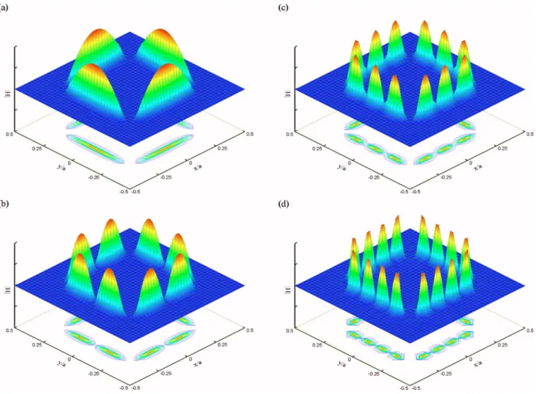
two-dimensional structure has a continuous interface which al-lows a degree of freedom to sustain the mode oscillation. Figure 12 shows the H field in magnitude for four typical surface phonon modes at the point⌫ near the surface phonon frequencysphfor a square array of square cylinders of half width w / a = 0.3. Note that in all the plots of the TE eigen-modes, the H field is normalized to have maximum unity, that is,兩H兩max= 1. Surface phonon modes may be as sharp as
a knife edge living on the interface. With the interfacial op-erator approach, it only takes a few points to resolve this feature. Note that in Fig. 12 the typical feature of the surface phonon modes is similar except a different variation along the interface. However, the eigenfrequency is almost identi-cal.
Apparently variation of the H field along the interface between the polar material and the dielectric does not alter the value of the eigenfrequency, and the interface can sustain as many stationary modes as it could. Consequently, there are expected to be infinite number of surface phonon modes around sph, analogous to the case of surface plasmon
modes.14,25The highly degenerate nature and infinite number
of surface phonon modes can be further explained through the Rayleigh quotient RH共32兲. It is known that the eigenfre-FIG. 12. 共Color online兲 The H field in magnitude for four typical surface phonon modes witha/2c=0.9286 at the point ⌫ near the surface phonon frequencysphfor a square array of square metallic cylinders关Fig. 1共b兲兴 of half width w/a=0.3, where Ta / 2c=0.4, La / 2c=1, and ⬁= 5.1.
quency corresponds to minimization of the Rayleigh quotient under a constraint that the corresponding eigenfunction be orthogonal to all previously obtained eigenfunctions. For a linear operatorL, Eq. 共32兲 can be used directly, while for a nonlinear operator, the Rayleigh quotient RH has to be ob-tained in a slightly different manner. Based on the interfacial operator approach developed in the previous section, we re-write the eigensystems共12兲 and 共14兲 in the dielectric and the polar material regions, respectively, as
⌳2H +⌳
冉
1 dⵜ2H冊
= 0, 共36兲 ⌳2H −⌳冉
⌳LH − 1 ⬁ⵜ2H冊
− ⌳T ⬁ⵜ2H = 0. 共37兲 Taking inner product of H with each term of the above two equations, adding them together, performing the integration by parts, and using the Bloch condition 共6兲, we obtain a quadratic expression for the Rayleigh quotient RH:RH 2 A − RHB + C = 0 共38兲 or, equivalently, RH= B ±
冑
B2− 4AC 2A , 共39兲 where A =冕
Vcell 兩H兩2d, B =冕
Sm H*Sda + 1 d冕
Vd 兩ⵜH兩2d+冕
Vm冉
1 ⬁兩H兩 2 +⌳L兩H兩2冊
d, C = −⌳T ⬁冕
Sm H*冏
H n冏
−da + ⌳T ⬁冕
Vm 兩ⵜH兩2d, 共40兲with Vd and Vmdenoting the volumes of the dielectric and the polar material, respectively, of the unit cell, and Smthe surface of Vm. In the expression of B, S appears in the sur-face integral term, which accounts for the contribution of the strength of surface phonon mode to the eigenfrequency. Note also that only the normal derivative of the H field occurs in the surface integral, and the tangential variation of the H field will not change the value of RHas well as the eigenfre-quency. There can be as many modes as possible if the varia-tion of the H field in the normal direcvaria-tion to the interface remains unchanged. This can be verified from the field pat-terns of the typical surface phonon modes in Fig. 12, which shows different degrees of oscillation along the interface. All the four modes have the same frequency a / 2c = 0.9286
with three significant digits. Surface phonon modes of higher oscillation can be resolved only when the grid resolution is fine enough to tell the tangential variation.
Another important aspect of surface phonon modes is band flattening and band broadening. The band flattening for the two-dimensional structures 关Figs. 1共b兲–1共d兲兴 is due to strong phonon-photon coupling that reduces the band dispersion.19 Basically, band flattening occurs for frequency
bands around the surface phonon frequency sphand
reso-nant cavity modes below the TO phonon frequency T. However, the shape/geometry of the polar material is a major factor in determining the overall band pattern. Figures 13 and 14 show the band structures for a square array of grid cylinders of thickness t / a = 0.1关Fig. 1共d兲兴. In particular, Fig. 14 shows that the flattened bands gathering around the sur-face phonon frequencysphspread more widely compared to
those of circular cylinders in Fig. 9. This is the phenomenon of band broadening, which is similar to the behavior of sur-face phonon modes for plasmonic crystals.25 This band
broadening is due to effective interaction of the modes on both sides of the polar material, which lifts the degeneracy. Moreover, the overall band structure for the grid cylinders exhibits a general flattening tendency, thus opening up wide photonic band gaps within the polariton gap共T⬍⬍L兲. As a comparison, Fig. 9 for round-shaped circular cylinders, shows that the frequency bands inside the polariton gap ex-tends widely in frequency, blocking the full gap region and denying opening up of photonic band gaps. On the other hand, the bands of resonant cavity modes for grid cylinders become more concentrated nearTbecause thin-striped po-lar materials allow less freedom in distributing the fields of FIG. 13. 共Color online兲 The TM band structure for a square array of grid cylinders 关Fig. 1共d兲兴 of thickness t/a=0.1 where Ta / 2c=0.4, La / 2c=1, and ⬁= 5.1. The dashed lines denote
the metallodielectric bands obtained by replacing the polar material with a perfect metal.
bulk modes. If the thickness ratio t / a or r / a is large, surface phonon modes are more densely distributed in frequency, while resonant cavity modes spread more widely.
3. Longitudinal modes
The electromagnetic fields are transverse in nature. How-ever, longitudinal modes may exist in a material when the dielectric constant becomes zero. According to the dielectric function共1兲 for polar materials, a longitudinal mode exists when its eigenfrequency is equal to the LO phonon fre-quency L. That also means oscillation of the electric field coincides with the coherent motion of the electrons. As with surface phonon modes, longitudinal modes appear only in the TE modes, for the transversality condition of the E field 共·E=0兲 is always met for the TM modes. However, longi-tudinal modes are difficult to obtain due to singularity of the operator in Eq.共4兲. Nevertheless, with rearrangement of the interfacial operator approach in Eq.共4兲, based on the dielec-tric function共1兲, the singularity is removed and longitudinal modes can be solved. Figure 15 shows the static mode at the point ⌫ for a square array of circular cylinders of radius
r / a = 0.3. Note that the longitudinal mode is constant in the
metal, which is the typical feature of longitudinal oscillation.
V. CONCLUDING REMARKS
In this paper, we proposed the interfacial operator ap-proach to compute band structures of polaritonic crystals or
photonic crystals of polar materials in one and two dimen-sions. In particular, an interfacial variable is introduced to measure the weighted difference of the normal derivatives of the H field across the interface, and thus accounts for the local strength of the surface phonon modes. Fine resolution at different grid levels shows that the mode frequencies are not very dependent upon the number of grid points except for the possible infinite degeneracy of surface phonon modes and the many resonant cavity modes. The number of re-solved resonant cavity modes and surface phonon modes do depend on the grid resolution.
The method has been applied to study four types of pho-tonic crystals of polar materials. In particular, we have ex-amined the effects of dimension, the size共filling ratio兲 effect, the effect of the intrinsic frequenciesT 共the transverse op-tical phonon frequency兲, and L 共the longitudinal optical phonon frequency兲 as well as the geometric 共shape兲 effect of the polar material. Physical details have been discussed re-garding the crossing and anticrossing schemes of band dis-persion, distribution of resonant cavity modes, localized na-ture of surface phonon modes, lifting degeneracy by thinning polar materials, and the limiting behaviors of the band struc-tures at the small limit ofTand large limit of L. Several interesting features were uncovered and explained and the main results were summarized in the Introduction. As a final remark, we have not considered the effect of dissipation of polaritonic structures which is substantial in the infrared re-gime. The issue is now under investigation, and the results will be reported elsewhere.
ACKNOWLEDGMENTS
This work was supported in part by National Science Council of the Republic of China under Contract Nos. NSC 94-2212-E-002-047 and NSC 94-2212-E-002-076, and the Ministry of Economic Affairs of the Republic of China under Contract No. MOEA 94-EC-17-A-08-S1-0006.
FIG. 14.共Color online兲 The TE band structure for a square array of grid cylinders 关Fig. 1共d兲兴 of thickness t/a=0.1, where Ta / 2c=0.4, La / 2c=1, and ⬁= 5.1. The dashed lines denote the metallodielectric bands obtained by replacing the polar material with a perfect metal.
FIG. 15.共Color online兲 The longitudinal mode at the point ⌫ for a square array of circular cylinders 关Fig. 1共c兲兴 of radius r/a=0.3 whereTa / 2c=0.4, La / 2c=1, and ⬁= 5.1.
*Electronic address: [email protected]
†Electronic address: [email protected] 1E. Yablonovitch, Phys. Rev. Lett. 58, 2059共1987兲. 2S. John, Phys. Rev. Lett. 58, 2486共1987兲.
3D. R. Smith, S. Schultz, N. Kroll, M. Sigalas, K. M. Ho, and C.
M. Soukoulis, Appl. Phys. Lett. 65, 645共1994兲.
4N. A. Nicorovici, R. C. McPhedran, and L. C. Botten, Phys. Rev.
E 52, 1135共1995兲.
5S. Fan, P. R. Villeneuve, and J. D. Joannopoulos, Phys. Rev. B
54, 11245共1996兲.
6T. Suzuki and P. K. L. Yu, Phys. Rev. B 57, 2229共1998兲. 7A. Moroz, Phys. Rev. B 66, 115109共2002兲.
8E. I. Smirnova, C. Chen, M. A. Shapiro, J. R. Sirigiri, and R. J.
Temkin, J. Appl. Phys. 91, 960共2002兲.
9C. C. Chang, J. Y. Chi, R. L. Chern, C. C. Chang, C. H. Lin, and
C. O. Chang, Phys. Rev. B 70, 075108共2004兲.
10A. R. McGurn and A. A. Maradudin, Phys. Rev. B 48, 17576
共1993兲.
11V. Kuzmiak, A. A. Maradudin, and F. Pincemin, Phys. Rev. B 50,
16835共1994兲.
12M. M. Sigalas, C. T. Chan, K. M. Ho, and C. M. Soukoulis, Phys.
Rev. B 52, 11744共1995兲.
13I. El-Kady, M. M. Sigalas, R. Biswas, K. M. Ho, and C. M.
Soukoulis, Phys. Rev. B 62, 15299共2000兲.
14T. Ito and K. Sakoda, Phys. Rev. B 64, 045117共2001兲. 15E. Moreno, D. Erni, and C. Hafner, Phys. Rev. B 65, 155120
共2002兲.
16I. I. Smolyaninov, W. Atia, and C. C. Davis, Phys. Rev. B 59,
2454共1999兲.
17G. Shvets and Y. A. Urzhumov, J. Opt. A, Pure Appl. Opt. 7, S23
共2005兲.
18M. M. Sigalas, C. M. Soukoulis, C. T. Chan, and K. M. Ho, Phys.
Rev. B 49, 11080共1994兲.
19W. Zhang, A. Hu, X. Lei, N. Xu, and N. Ming, Phys. Rev. B 54,
10280共1996兲.
20V. Kuzmiak, A. A. Maradudin, and A. R. McGurn, Phys. Rev. B
55, 4298共1997兲.
21K. C. Huang, P. Bienstman, J. D. Joannopoulos, K. A. Nelson,
and S. Fan, Phys. Rev. Lett. 90, 196402共2003兲.
22C. Kittel, Introduction to Solid State Physics, 7th ed.共John Wiley
& Sons, New York, 1996兲.
23O. Toader and S. John, Phys. Rev. E 70, 046605共2004兲. 24A. Modinos, N. Stefanou, and V. L. Yannopapas, Opt. Express 8,
197共2001兲.
25C. C. Chang, R. L. Chern, C. C. Chang, and R. R. Hwang, Phys.
Rev. B 72, 205112共2005兲.
26L. D. Landau and E. M. Lifshitz, Quantum Mechanics
共Perga-mon, New York, 1977兲.
27G. Shvets, Phys. Rev. B 67, 035109共2003兲.
28K. C. Huang, P. Bienstman, J. D. Joannopoulos, K. A. Nelson,