158 IEEE ELECTRON DEVICE LETTERS, VOL. 29, NO. 2, FEBRUARY 2008
High-Speed GaN-Based Green Light-Emitting
Diodes With Partially n-Doped Active Layers
and Current-Confined Apertures
J.-W. Shi, J.-K. Sheu, C.-H. Chen, G.-R. Lin, and W.-C. Lai
Abstract—We demonstrate a high-speed GaN-based green
light-emitting diode for plastic optical fiber (POF) communication applications. By using a combination of n-type doping and undoped InxGa1−xN/GaN based multiple quantum wells (MQWs), and a 76-µm-diameter current-confined aperture structure, we can ob-tain an extremely high electrical-to-optical (E–O) 3 dB bandwidth (∼330 MHz), which is limited by the spontaneous recombination lifetime of the MQWs. A reasonable coupled power (∼264 µW) can be simultaneously achieved for a 2 mm in diameter POF with a 0.5 numerical aperture (NA).
Index Terms—GaN, LED, optical fiber.
I. INTRODUCTION
H
IGH-SPEED red LEDs [1] often serve as key transmit-ter components for communication networks using plas-tic opplas-tical fibers (POFs). According to the media-oriented sys-tems transport (MOST) standard they must run at a data rate of 22.5 Mb/s [2]. However, the optical bandwidth of the red oper-ating window (∼650 nm) of the current commercially used polymethylmethacrylate (PMMA) POF is narrower, and the propagation loss higher (0.125 dB/m vs. 0.09 dB/m) than that of the high-performance POF system [3]. This operates under a PMMA loss minimum window, which has a wavelength of around 500 nm [3]. The III-nitride-based green LEDs would thus be a more promising choice for such applications [4]. Al-though the material dispersion of the PMMA fiber at around 520 nm wavelength is higher (1.5 times higher) than at 650 nm wavelength, the dispersion-free window in the total dispersion spectrum, which includes the waveguide dispersion and the material dispersion, may be shifted to 520 nm by optimiz-ing the index profile of the PMMA fiber [5]. In this letter, we demonstrated an InxGa1−xN/GaN-based high-speed greenLED with a current-confined aperture and partial n-type dop-ing InxGa1−xN/GaN-based multiple quantum wells (MQWs).
Manuscript received August 17, 2007; revised November 15, 2007. The review of this letter was arranged by Editor P. Yu.
J.-W. Shi and C.-H. Chen are with the Department of Electrical Engineer-ing, National Central University, Taoyuan 320, Taiwan, R.O.C. (e-mail: jwshi@ ee.ncu.edu.tw; [email protected])
J.-K. Sheu and W.-C. Lai are with the Institute of Electro-Optical Sci-ence and Engineering, Advanced Optoelectronic Technology Center, National Cheng Kung University Tainan 70101, Taiwan, R.O.C. (e-mail: jksheu@mail. ncku.edu.tw; [email protected]).
G.-R. Lin is with the Graduate Institute of Electro-Optical Engineering, De-partment of Electrical Engineering, National Taiwan University, Taipei 10617, Taiwan, R.O.C. (e-mail: [email protected])
Color versions of one or more of the figures in this letter are available online at http://ieeexplore.ieee.org.
Digital Object Identifier 10.1109/LED.2007.914070
With this device, one can achieve an extremely high electrical-to-optical (E–O) 3-dB bandwidth (∼330 MHz), limited only by the spontaneous lifetime of our MQWs, with a reasonable POF coupling power (∼264 µW) suitable for POF communications.
II. DEVICESTRUCTURE ANDFABRICATION
The LED wafers were grown by metal–organic chemical va-por deposition (MOCVD) on a sapphire substrate. The active region of the LED was a ten-period InxGa1−xN/GaN based
MQW structure, which consists of a 135- ˚A-thick GaN barrier layer and a 25- ˚A-thick InxGa1−xN well layer in each period.
The n-type doping density was around 5× 1017cm−3in seven of the GaN barrier layers near the n-type cladding layer. Con-versely, the barrier layers near the p-type cladding layer were left undoped. Although n-type doping in the InxGa1−xN/GaN
based MQW layers can improve the material quality and the radiative recombination rate [4] in MQWs, this approach may result in most of the depletion region being located in the p-type GaN layers as the doping density in the MQW layers is com-parable to the typical ionized doping density of the p-type GaN layer [6]. By inserting three undoped MQW periods near the p-side of the active region, the external electric field can be con-centrated more in the active layers than is the case when fully n-type doped MQWs are used in the active layers. Compared with GaN LEDs with fully n-doped MQWs [4] under the same bias voltage, higher output power performance of demonstrated partially n-doped LEDs can, thus, be expected. For high-speed applications, a current-confined aperture was realized by etch-ing a small mesa on the topmost p-type GaN layer to restrict the current-flow path and reduce the capacitance [1], [7]. The use of a current-confined aperture can eliminate etching-induced damage on the MQW sidewall and its influence on the internal quantum efficiency of LEDs, such as what occurs with direct etching through the active MQW layers to reduce capacitance. A conceptual cross-sectional view of demonstrated device and the top view of the current-confined aperture is given in Fig. 1 and its inset. In order to study the influence of the diameter of the current-confined aperture on the speed and output power performance of the LEDs, devices with different diameters of current-confined aperture and active areas were fabricated. The epilayers and geometric structure of devices A–D were simi-lar, with only the ratio of the diameter of the current-confined aperture to that of total circular active mesa of the bottom side being varied. The ratios of devices A and B are 1:1 and 1:2, respectively. For devices C and D, the ratio is the same at 1:3. The diameter of the circular active area below the p-type GaN
0741-3106/$25.00 © 2008 IEEE
SHI et al.: HIGH-SPEED GaN-BASED GREEN LIGHT-EMITTING DIODES 159
Fig. 1. Conceptual cross-sectional view of the demonstrated LED. The inset shows the top view of device after zooming in on the active current-confined aperture. For clearness, the figure was not drawn according to scale.
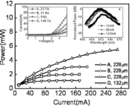
Fig. 2. Output optical power (P) versus the bias current (I) of the devices (A– D) measured with different diameters of current-confined apertures. The two insets show the measured I–V curves of devices A–D and electroluminescence (EL) spectra of device A measured under different bias currents.
layer is 228 µm, the same as for devices A–C. Device D has a diameter of 132 µm. As shown in Fig. 1, the LED unit was integrated with two coplanar waveguide (CPW) pads [4], which were parallel to the uniform current distribution during the dc measurement. Alternatively,for the ac measurement, one of the CPW pads was left as RFs open. Details of the fabrication pro-cesses of the demonstrated devices can be referred to in our previous paper [4].
III. MEASUREMENTRESULTS ANDDISCUSSION
During dc measurement, the output power of the LED was collected by use of an integrating sphere or a POF (2 mm in di-ameter and with a 0.485 NA), which served as an optical probe. All four devices exhibited similar bias-dependent electrolumi-nescence (EL) spectra behavior with a similar center wavelength (∼510 nm). The inset of Fig. 2 shows the EL spectra of device A measured under different bias currents. A slight blue shift of the center wavelengths (∼510 to ∼500 nm) was observed when the bias current increased from 10 to 100 mA, which can be attributed to the screening of the piezoelectric field and the renormalization of the quantized states in the well region under a forward bias [4]. Another inset of Fig. 2 shows the current– voltage (I–V) curves of devices A–D. The turn-ONvoltages of these four devices were all around∼3 V. The values of the
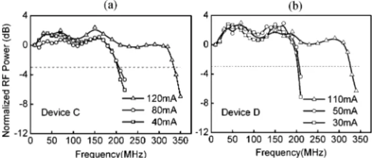
differ-Fig. 3. E–O frequency responses of (a) device A and (b) device B measured under different bias currents.
ential resistances of each device are also specified in this inset. We can clearly see, via the difference in the cross-sectional ar-eas of the current-flowed paths, that device A has a much lower differential resistance than device D. Fig. 2 shows the optical power (P) collected by use of the integrating sphere versus the injected current (I) for the four devices. We can clearly see that device A has a much higher saturation output power than that of devices B–D. This is due to their much smaller light-emitting area, much larger differential resistance, as shown in the inset to Fig. 2, and more serious device heating effect than device A. By measuring the difference in collected optical power, ob-tained using an integrating sphere and a POF, we can obtain the coupling efficiency of the devices: this was the same for all four devices, around 13.4%, which is close to the reported coupling efficiency (∼11%) for high-speed GaN based green LEDs to POFs [3]. The similar coupling efficiency of all of our devices can be ascribed to the fact that their output far field is similar and can be approximated by an ideal Lambertian far-field distribution regardless of the diameter of the light-emitting aperture [8]. Even device C, with its small light-emitting area, had a coupled optical power (185 µW under 50 mA) to the POF large enough for POF communication [3]. Using the same measurement setup and the same bias current (∼100 mA) as in our previous paper, we found the POF-coupled optical power of the current LED (device B) to be much higher (343 µW vs. 170 µW) than that of our previous fully n-type doped MQW green LED, even though it had a larger active area (∼14000 µm2
vs.∼10000 µm2) [4]. As can be seen in Fig. 2, the P–I
mea-surement results are superior to those found in our previous pa-per [4], which implies the advantages of using partially n-doped MQW structures. During the ac measurement, we injected the RF signal into the LEDs. The modulated optical power was collected by the POF and then fed into a low-noise Si-based photoreceiver (New Focus: 1801) that was connected with an RF spectrum analyzer. We only deembedded the frequency re-sponse of the photoreceiver because the microwave loss for the K-band passive RF components used in the frequency range of interest (hundreds of megahertz) for LED measurement is negli-gible. Fig. 3(a) and (b) and Fig. 4(a) and (b) show the measured E–O frequency responses under different bias currents obtained for devices A–D. The maximum bias current is limited by device failure. We can clearly see that the measured 3 dB bandwidth of each device increases significantly with a bias current den-sity. This phenomenon has been reported for other LEDs and
160 IEEE ELECTRON DEVICE LETTERS, VOL. 29, NO. 2, FEBRUARY 2008
Fig. 4. E–O frequency responses of (a) device C and (b) device D measured under different bias currents.
can be attributed to the bimolecular recombination probability being proportional to the injected carrier density into the active volume [8], [9]. Devices C and D have a bias current of around 100 mA and a very high current density (>2.2 kA/cm2), and both could exhibit a 3 dB bandwidth as high as 330 MHz. The coupled optical power of device C under high-speed operation was around 264 µW. To the best of the authors’ knowledge, this is the highest 3-dB modulation bandwidth (330 MHz) ever re-ported for III-nitride-based LEDs [3], [4]. Such a value is compa-rable with the highest reported 3 dB bandwidth (300–500 MHz) for AlGaInP-based red resonant cavity LEDs (RCLEDs) [1]. There are two major factors limiting the speed of LEDs: one is the RC time constant and the other is the spontaneous recombi-nation time. In order to clarify which one caused the significant bandwidth enhancement observed for devices C and D, we per-formed capacitance–voltage (C–V) and current–voltage (I–V) measurements to obtain the RC-limited bandwidths of the de-vices. The extracted RC-limited bandwidth, which includes the 50-Ω source resistance, of devices A, C, and D were around 150 MHz, 1 GHz, and 3 GHz, respectively. Such a result indi-cates that the current-confined aperture can effectively reduce the diffusion capacitance and improve the RC-limited band-widths. According to the extracted RC-limited and measured 3 dB bandwidths of the devices, we can conclude that under a high bias current density, the dominant bandwidth limiting fac-tor of device A is the RC delay time, and for devices C and D, it is the spontaneous recombination time and the maximum al-lowable bias current density. A higher speed performance (near 1 GHz) [1], [9], [10] may be expected by decreasing the thick-ness of the active layer (MQW) (by increasing the injected carrier density) [1], [9], [10], using the fully doped MQWs structure at the expense of lower output power [1], [4], [10], or further minimizing the device resistance and heating effect to increase the maximum allowable bias current density. Based on
the measured 3 dB bandwidth (330 MHz), the extracted recom-bination time will be around 0.5 ns [9], which is a reasonable number and comparable to the measurement results (∼1 ns) for fully n-type doped InGaN/GaN-based MQWs obtained using the time-resolved photoluminescence technique [11].
IV. CONCLUSION
We demonstrate a GaN-based high-speed green LED. By uti-lizing a current-confined aperture with partially n-doped MQW active layers, we can simultaneously achieve a 330-MHz 3-dB E–O bandwidth with a reasonable (∼264 µW) POF optical cou-pling power. Such an excellent high-speed performance can be attributed not only to an increase of the bias current density but also to a reduction of device capacitance through the use of the current-confined structure.
REFERENCES
[1] R. Wirth, B. Mayer, S. Kugler, and K. Streubel, “Fast LEDs for poly-mer optical fiber communication at 650 nm,” in Proc. SPIE, vol. 6013, Bellingham, WA, 2005.
[2] MOST Cooperation, Specification Rev. 2.4, May 2005.
[3] M. Akhter, P. Maaskant, B. Roycroft, B. Corbett, P. de Mierry, B. Beaumont, and K. Panzer, “200 Mbit/s data transmission through 100 m of plastic fiber with nitride LEDs,” Electron. Lett., vol. 38, pp. 1457–1458, Nov. 2002.
[4] J.-W. Shi, H.-Y. Huang, J.-K. Sheu, C.-H. Chen, Y.-S. Wu, and W.-C. Lai, “The improvement in modulation speed of GaN-based light-emitting diode (LED) by use of n-type barrier doping for plastic optical fiber (POF) communication,” IEEE Photon. Technol. Lett., vol. 18, no. 15, pp. 1636– 1638, Aug. 2006.
[5] G. Yabre, “Theoretical investigation on the dispersion of graded-index polymer optical fibers,” J. Lightw. Technol., vol. 18, no. 6, pp. 869–877, Jun. 2000.
[6] S. Nakamura, M. Senoh, and T. Mukai, “Highly P-typed Mg-doped GaN films grown with GaN buffer layers,” Jpn. J. Appl. Phys., vol. 30, no. 2, pp. L1708–L1711, Oct. 1991.
[7] M. Kneissl, T. L. Paoli, P. Kiesel, D. W. Treat, M. Teepe, N. Miyashita, and N. M. Johnson, “Two-section InGaN multiple-quantum-well laser diode with integrated electro-absorption modulator,” Appl. Phys. Lett., vol. 80, pp. 3283–3285, May 2002.
[8] P. Bhattacharya, Semiconductor Optoelectronic Devices. Taipei, Taiwan: Pearson Education, 2003, pp. 216–218.
[9] K. Ikeda, S. Horiuchi, T. Tanaka, and W. Susaki, “Design parameters of frequency response of GaAs-(Ga,Al)As double heterostructure LED’s for optical communications,” IEEE Trans. Electron Devices, vol. ED-24, no. 7, pp. 1001–1005, Jul. 1977.
[10] R. Windisch, A. Knobloch, M. Kuijk, C. Rooman, B. Dutta, P. Kiesel, G. Borghs, G. H. D¨ohler, and P. Heremans, “Large-signal-modulation of high-efficiency light-emitting diodes for optical communication,” IEEE
J. Quantum Electron., vol. 36, no. 12, pp. 1445–1453, Dec. 2000.
[11] M. S. Minsky, S. Chichibu, S. B. Fleischer, A. C. Abare, J. E. Bowers, E. L. Hu, S. Keller, U. K. Mishra, and S. P. Denbaars, “Optical properties of InGaN/GaN quantum wells with Si doped barriers,” Jpn. J. Appl. Phys., vol. 37, no. 2, pp. L1362–L1364, Nov. 1998.