國
立
交
通
大
學
資訊工程系
碩 士 論 文
嵌入式處理器上的第一階層指令
快取記憶體之漏電流管理
Leakage Management for On-Chip L1
Instruction Cache in Embedded Processor
研 究 生:賴 敬 中
指導教授:單 智 君 博士
嵌入式處理器上的第一階層指令
快取記憶體之漏電流管理
Leakage Management for On-Chip L1
Instruction Cache in Embedded Processor
研 究 生:賴 敬 中
Student:Ching-Zhong Lai
指導教授:單 智 君 博士 Advisor:Dr. Jean, Jyh-Jiun Shann
國 立 交 通 大 學
資 訊 工 程 學 系
碩 士 論 文
A Thesis
Submitted to Department of
Computer Science and Information Engineering
College of Electrical Engineering and Computer Science
National Chiao Tung University
in Partial Fulfillment of the Requirements
for the Degree of
Master
In
Computer Science and Information Engineering
August 2005
Hsinchu, Taiwan, Republic of China
嵌入式處理器上的第一階層指令
快取記憶體之漏電流管理
學生:賴敬中 指導教授:單智君 博士 國立交通大學資訊工程學系碩士班摘要
由於許多嵌入式系統有使用電池的需求,低功率設計能夠延長電池的使用壽 命,已經成為一項重要的議題。當製程技術持續進步變得越來越小時,因關閉狀 態的電晶體所造成的漏電流之耗電將會變成晶片上的主要電耗。再嵌入式處理器 上的第一階層快取記憶體佔據處理器上大量的電晶體數目,因此很多的漏電流電 耗是消耗在此快取記憶體上。由於區域性的理由,在某一段時間內只有少部分的 快取記憶體會被用到的,快取記憶體中的大部分是最近不會使用到的,可以將之 放到低功率模式來降低漏電流功率。先前的漏電管理中,沒有使用預先開啟的機 制或是只有簡單的機制來將還在低功率模式的快取記憶體區塊預先開啟;而且其 關閉的機制都是在等一段長期的時間後才會關閉不用的快去記憶體區塊。我們提 出一個準確的預先開起機制,來避免喚起低功率模式快取記憶體區塊所需的延遲 時間,以及一個更積極的關閉記憶體機制來得到更多的漏電能量減少。我們所提 出的設計可以改善先前的設計的 18%~23%。Leakage Management for On-Chip L1
Instruction Cache in Embedded Processor
Student:Ching-Zhong Lai Advisor:Jean, J.J Shann
Institute of Computer Science and Information Engineering National Chiao Tung University
Abstract
Since requirement of battery usage in many embedded systems, low power design trends to increase life time and has become an important issue for embedded processor design. When the technology continues to scales down, the leakage power due to leakage current in ‘off’ state transistors will become the domination of chip’s power consumption. On-chip L1 cache consist a major portion of embedded processor’s transistor budget, thus much leakage power is consumed in on-chip cache. For locality reasons, only a small part of cache will be accessed in a time period, most parts of cache that will not be accessed recently can be placed into low power mode to reduce leakage power. Previous leakage managements in instruction cache have either none or a simple pre-activation scheme that pre-activate low power mode cache line and turn off cache lines after a large period time. We propose an accuracy pre-activation policy to avoid wake-up latency and a simple and aggressive turn-off policy to obtain more leakage energy reduction in instruction cache. Our proposed design has about 18% ~ 23% of improvement on previous works.
誌謝
本論文得以完成,首先要感謝 單智君教授的辛勤指導與嚴格的督促,同時 感謝實驗室的另一位指導老師 鍾崇斌教授,多次提出批評與指正,使得論文更 加嚴謹。在口試時,亦要感謝 盧能彬教授所提出的寶貴意見,使得這篇論文更 臻完整。 此外,要感謝實驗室博士班謝萬雲、鄭哲聖與喬偉豪學長,對於我的研究提 出問題並給予建議。還有,感謝實驗室的學長姐、同學以及學弟們的幫忙,不論 是資料蒐集、程式技巧和寫作要點的討論等,都給予我莫大的助益,有你們的陪 伴,更使我的研究生活更加充實與豐富。 最後,我要感謝我的家人與好友長期地給予我支持與鼓勵,使我在兩年的碩 士生涯中,能無後顧之憂地投入課業與研究之中。 — 謹將此論文獻給所有關心我、愛護我的師長及親朋好友— 謝謝你們
賴敬中 2005/8/29 計算機系統實驗室Table of contents
摘要 ... i
致謝 ... ii
Abstract ... iii
List of Figures... vi
List of Tables... viii
Chapter 1 Introduction ...1
1.1 Research Motivations ...2
1.2 Research Objective ...3
1.3 Organization of This Thesis ...3
Chapter 2 Background and Related Work ...5
2.1 Leakage Current...5
2.2 State Destructive Technique...7
2.2.1 DRI I-cache...8
2.2.2 Cache Decay ...9
2.3 State Preserving Technique... 11
2.3.1 Drowsy Cache...13
2.3.2 Drowsy Insturction Cache ...14
2.3.3 HotSpot Leakage Management & Just-In-Time Activation ...16
2.3.4 Compiler Approach...19
2.3.5 Summary and Observation...20
Chapter 3 Proposed Design of Leakage Management on L1 cache...22
3.1 Two-Direction Pre-activation...22
3.1.1 Pre-activate Sequential Line (SL)...23
3.1.3 Pre-activate Sequential Set (SS) ...27
3.1.4 Pre-activate Jump Line (JL)...27
3.1.5 Pre-activate Jump Line of Next Accessed Line (NJL) ...28
3.1.6 Summary of Two-Direction Pre-activate Schemes...28
3.2 MRU-Keeping Turn-off Policy...30
3.3 Circuit Block of Our Proposed Design ...31
Chapter 4 Simulation Environment and Experiment Result ...35
4.1 Simulation Environment ...35
4.2 Power Model...38
4.3 Experiment Results and Analysis ...41
4.3.1 Evaluation of Pre-activation schemes and MRU Buffer Size...41
4.3.2 Experiment Results Compared with Previous Work ...45
4.3.1 Discussion ...46
Chapter 5 Conclusion ...50
List of Figures
Figure 1-1 The ratio of dynamic power to static power...2
Figure 2-1 Total chip dynamic and static power dissipation trends based on the ITRS ...6
Figure 2-2 Gated-Vdd technique ...8
Figure 2-3 DRI I-cache’s anatomy...9
Figure 2-4 Cache generations in a reference stream ...10
Figure 2-5 The hierarchical counter mechanism ... 11
Figure 2-6 Implementation of the drowsy cache line by multiple supply voltage...12
Figure 2-7 Next sub-bank prediction buffer ...14
Figure 2-8 Next sub-bank predictor in cache tags ...15
Figure 2-9 Just-In-Time Activation scheme...16
Figure 2-10 HotSpot based Leakage Management scheme ...18
Figure 2-11 The control flow graph of conservative strategy and optimistic strategy...20
Figure 3-1 The concept of two-direction pre-activation ...23
Figure 3-2 Pre-activate sequential line ...23
Figure 3-3 Late pre-activation case of SL pre-activation ...24
Figure 3-4 Pre-activate sequential line of next accessed line ...25
Figure 3-5 An example of NSL pre-activation ...26
Figure 3-6 Pre-activate sequential set (JITA scheme)...27
Figure 3-7 Pre-activate jump line ...28
Figure 3-8 Pre-activate jump line of next accessed line ...29
Figure 3-10 A reference stream of some one cache line...30
Figure 3-11 MRL-Keeping buffer (updated by LRU policy) ...31
Figure 3-12 The circuit block of JL-SL pre-activation policy ...32
Figure 3-13 The update policy of JL-SL pre-activation policy ...33
Figure 3-14 The circuit block of NJL-NSL pre-activation polic ...34
Figure 3-15 The update policy of NJL-NSL pre-activation policy...34
Figure 4-1 The situation that NJL may be better than JL pre-activation ...43
Figure 4-2 I-cache leakage energy with different pre-activation scheme in 4-entry MRU buffer ...44
Figure 4-3 I-cache leakage energy with NJL-SS and NJL-SL pre-activation ...44
Figure 4-4 I-cache leakage energy of our design and previous works ...46
Figure 4-5 Improvement over previous work ...47
List of Tables
Table 2-1 Energy parameters and drowsy transition time for 32-KB 4 way
set associative cache with 32Wmin for voltage controller size ...12
Table 2-2 Summary of previous work and our proposed design ...21
Table 4-1 Configuration Parameters of SimpleScalar/ARM ...35
Table 4-2 MiBench Benchmarks ...38
Table 4-3 Simulation parameters ...40
Table 4-4 Pre-activation accuracy in two-direction pre-activation...42
Chapter 1 Introduction
Low power design has become more and more importance in microprocessor designs, especially in the embedded system. Battery lifetime is an important consideration in portable devices of embedded system, such as MP3 player, mobile phone, Personal Digital Assistants (PDAs), handheld game player etc. In additional to battery lifetime, heat will cause the system to become un-reliability and need heat removal expense. Low power designs can reduce energy consumption and operation temperature to increase the battery lifetime and system reliability.
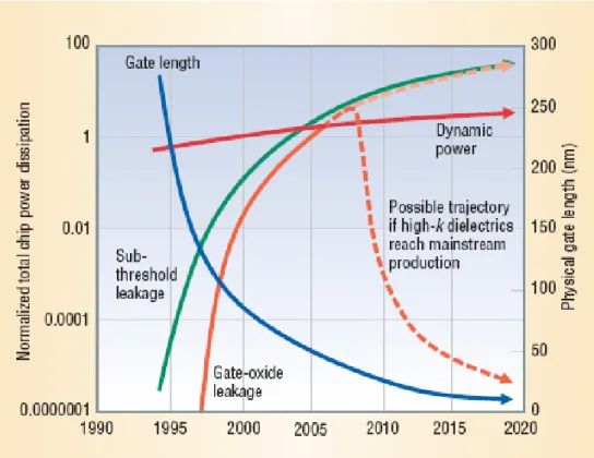
The power consumption of CMOS transistors consists of dynamic power and static power. The dynamic power (switching power, active power) consumption is dissipated by charging and discharging the output capacitance due to switching activity, and the static power (leakage power) is dissipated by leakage current that leaks through transistors when they are in their ‘off’ state. The leakage power of CMOS transistors is negligible when not switching, and the switching power is the domination of the total power consumption in the past technology. However, when the technology continues to scales down, the static power will become the domination of total power consumption. Figure 1-1 [1] illustrates the proportion of dynamic power and static power of total power consumption. In the newly technology (90nm), about half of power consumption is dissipated by static power, and static power will occupies more and more ratio in the future. Leakage power reduction will become an important issue of low power design in the future technology.
Leakage energy consumption is a problem for all transistors, and L1 on-chip caches consists a major portion of embedded processor’s transistor. For instance, 60% of core is devoted to cache and memory structure on StrongARM processor. For locality reasons, only a small part of cache will be accessed in a time period, most
parts of cache that will not be accessed recently can be placed into low power mode to reduce leakage energy consumption.
Since the leakage current is a function of the supply voltage, leakage energy can be reduced by reducing the supply voltage. There is an effective circuit technique proposed in [2] that two supply voltages can be dynamically switched for the SRAM cells. In this technique, cell’s data can be preserved in drowsy mode of lower supply voltage, and cell’s data can be accessed in active mode of normal supply voltage. Our research is based on this circuit technique to manage the power mode of L1 instruction cache.
Figure 1-1. The ratio of dynamic power to static power source: EE-Times, 08/06/2004
1.1 Research Motivation
There is a small wake-up time (one or two cycle) from drowsy mode to active mode, this wake-up time penalty may occur pipeline stalls to significantly consume extra processor energy. For this reason, turn-on policy need to pre-activate the drowsy
cache line before assessed. In instruction cache, the access pattern is either sequential or taken branch. Previous pre-wakeup scheme only utilizes sequential access patterns to pre-active sequential set of current accessed cache line, the jump line due to taken branch should be pre-activated to decrease the wake-up penalty.
There is extra dynamic energy consumption for power mode transition. To turn off the cache lines which will be accessed again recently may be no worth. For this reason, turn-off policy need to turn off most cache lines which will be not accessed again recently, and avoid some cache lines that will be accessed again soon being non-beneficially turned off. In previous works, cache lines will be turned off after a large fixed period, in fact, some cache lines may be turned off earlier to obtain more leakage energy reduction.
1.2 Research Objective
The goal of cache leakage management is that to pre-activate drowsy cache line before accessed, and to turn off the cache lines which will not be accessed again soon. For turn-on policy, we exploit the access patterns of instruction cache which is either sequential or taken branch to pre-activate sequential and jump (due to taken branch) lines to avoid wake-up penalty; and for turn-off policy, to turn off the most cache lines which are not recently accessed.
1.3 Organization of This Thesis
The rest of this thesis is organized as follows. Chapter 2 introduces the background of circuit technique to support low power mode cache, and discuses the related works of power mode management based on these circuit techniques. In Chapter 3, we propose our instruction cache leakage management which consists of
two-direction pre-activation scheme and MRU-Keeping turn-off policy. The experiment environment and results are presented in Chapter 4. Finally, we summarize our conclusion in the Chapter 5
Chapter 2 Background and Related Work
In this chapter, we first introduce the background of leakage current. And then we introduce two circuit techniques which are state destructive and state preserving techniques for cache leakage reduction, and introduce some management schemes based on these circuit techniques. Finally, we will discuss these related works of the low power mode management, and propose our idea of instruction cache leakage management scheme.
2.1 Leakage Current
Figure 2-1 shows the dynamic and static power consumption trend based on 2002 statistics normalized to the 2001 International Technology Roadmap for
Semiconductors (ITRS) [3]. The ITRS projects a decrease in dynamic power per
device over time. However, it assume a doubling of on-chip devices every two years, thus total dynamic power will slightly increase on per-chip basis. The leakage power increases rapidly, and will surpass the dynamic power soon. Leakage power is consumed by leakage current of transistors, and there are two principle components of leakage current:
Subthreshold leakage, a weak inversion current across the device.
Gate leakage, a tunneling current through the gate oxide insulation (will equal to subthreshold in 2005).
First, the subthreshold leakage has been formularized by [4] as below:
(1) / / 1
(1
)
th V nkT V kT subI
=
K We
−−
e
−Figure 2-1. Total chip dynamic and static power dissipation trends based on the International Technology Roadmap for Semiconductors (ITRS).
The subthreshold leakage increases exponentially with the lowering of threshold voltage, Vth, the higher of temperature, T, and is proportional to gate width, W.
Utilizing high Vth to reduce the subthredhold leakage, but high Vth will increase
operation latency. Furthermore, to disconnect or reduce the supply voltage also can obtain the significant leakage reduction.
Second, a simplification of equation from [4] is sufficient to illustrate the key points:
(2)
The gate leakage increases exponentially with decrease of Tox (Thickness of Gate Oxide), decrease of supply voltage, V, and is proportional to the gate width, W. It is highly dependent on the Tox and supply voltage. Increasing the Tox will reduce the gate leakage; unfortunately, it also degrades the transistor’s effectiveness. This
2 / 2 ox T V ox ox
V
I
K W
e
T
α −⎛
⎞
=
⎜
⎟
⎝
⎠
problem can be solved by high-k materials (2010). On the other hand, reduction the supply voltage is an effective approach to reduce the gate leakage energy.
There are many circuit techniques such as multithreshold CMOS (MTCMOS) circuit technique [5], dual-threshold voltage technique [6], variable threshold voltage technique [7], gated-Vdd technique [8], and multiple supply voltage (or DVS: dynamic
voltage scaling) technique [2] etc. for leakage power reduction. Here, we introduce the two newly circuit technique of state destructive and state preserving technique that utilizing gated-Vdd and multiple supply voltage to reduce the leakage energy.
2.2 State Destructive Technique
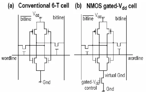
Figure 2-2 illustrates gated-Vdd circuit technique [8] [9] in the 6T SRAM cell
that using a extra high-Vth transistor in the supply voltage (Vdd) or the ground path
(Gnd) of the cache’s SRAM cells, the cell’s supply voltage is “gated” when the extra transistor is turned off. This gated-Vdd technique can achieve significantly low
leakage due to the stacking effect [10] that two off transistors connected in series reduce the subthreshold leakage current by orders of magnitude due to the self reverse-biasing of stack transistor. Furthermore, this technique will lose any information stored in the cell when switched into low-leakage mode. It means that it will bring about extra cache misses to access low hierarchical memory and incur significant performance penalty.
Figure 2-2. The 6T SRAM cell: (a) conventional, (b) with NMOS gated-Vdd
2.2.1 DRI I-cache
The concept of this management scheme is that there is a large variability in instruction cache utilization both with and across programs leading to large inefficiency in conventional caches. The DRI I-cache [9] [10] dynamically resizes the instruction cache by monitoring the cache miss rate and the disable portion of the cache are placed into sleep mode to obtain leakage power reduction.
This technique is based on gated-Vdd to implement the sleep mode. Figure 2-3
depicts the anatomy of the DRI instruction cache. There is a miss counter to recode the amount of cache miss, and circuit will monitor the miss counter in a fixed-length
sense interval such as one million dynamic instructions. As the end of each sense
interval, to compare the miss counter with a pre-defined miss-bound and then upsize or downsizes the cache depending on the miss counter is lower or higher than the miss-bound. When resizing the cache, to increase double of current active cache size or decrease half of current active cache size. In order to avoid thrashing, the DRI instruction cache never downsize beyond a pre-defined size-bound value. The index
mask is used to map the different size of instruction cache dynamically. Furthermore, all the cache parameters such as miss-bound, sense interval, and size-bound also can set either dynamically or statically.
Figure 2-3. DRI I-cache’s anatomy [9]
Since the different cache size requires different tag bits, this technique needs to store the large tag bits for the correspondingly smallest size of cache. Thus it requires maintaining more tag bits than conventional cache of equal size. Furthermore, resizing cache need data remapping, thus incurs extra compulsory misses after resizing cache. It was reported that this technique will lead to large performance penalties in some application.
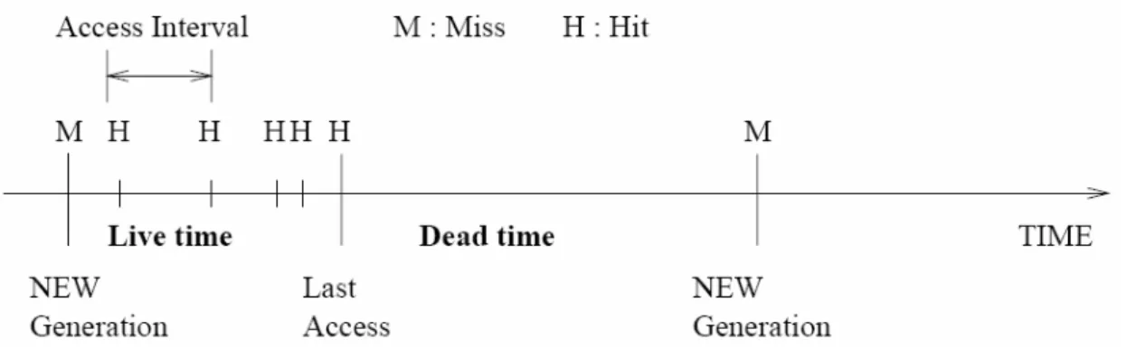
2.2.2 Cache Decay
Figure 2-4 depicts a stream of references to a particular cache line. When a cache miss occurs, a new generation comes into beginning, and it ends when this line is replaced. Each generation is comprised of a series of reference to the cache line. The
time between the last access to a cache line and its eviction is called “dead time”.
Figure 2-4. Cache generations in a reference stream
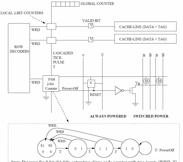
To turn off the cache lines in its dead time by state-destructive technique can obtain leakage power reduction. When a cache line has not been accessed for a long time (decay interval) it may be in its dead time that its data is no needed. The cache decay [11] policy adopt this concept that using a cycle counter for each cache line to record its no-access period and turn off it if the counter is saturated (achieves decay interval). The decay intervals should be in the range of tens of thousands of cycles according to their experiment. The cycle counter for each cache line has many bits ( log2(decay interval) ) such that make it impractical to implement. The solution is to
utilize a hierarchical counter mechanism where a single global counter which counts per cycle provides the ticks for a smaller local counter of each cache line. This mechanism is shown in figure 2-5.
For different applications, it may be needed to select an adaptive decay interval to make the cache decay policy do better. There are some adaptive version of cache decay scheme has been proposed in [11][12][13].
Figure 2-5. The hierarchical counter mechanism
2.3 State Preserving Technique
Another opposite circuit technique is state preserving technique. Figure 2-6 shows the multiple supply voltage approach [2] [14] to implement state preserving technique. Two different supply voltages can be selected dynamically for the SRAM cells (a cache line or a sub-bank). It assumes that the threshold voltage of 70nm technology is ~ 200 mV, and to set the standby voltage 50% higher than the threshold voltage. The main additions are a drowsy bit which is a mechanism for controlling the supply voltage to the SRAM cells, a word-line gating circuit of AND gate, and tow
prevent from accessing the cache line in drowsy mode, since the supply voltage of the drowsy cache line is lower than the bit line precharge voltage; accessing a drowsy cache line could destroy the cell’s contents.
Figure 2-6. Implementation of the drowsy cache line by multiple supply voltage
In this circuit technique, to place the SRAM cells into drowsy mode (lowest supply voltage) can obtain a significant leakage power reduction due to the decrease in both leakage current and supply voltage, and data in the SRAM cell will not lose in drowsy mode. Furthermore, the latency of supply voltage transition is small thus the drowsy cache line can be waked up in a cycle time. The transition delay time depends on the PMOS transistor width of the pass gate switch in the voltage controller. More large width has more small latency and more large transition energy consumption. Table 2-1 [2] lists the detail power parameters.
Table 2-1 [2]. Energy parameters and drowsy transition time for 32-KB 4 way set associative cache with 32Wmin for voltage controller size
1.63E-15J 2.59E-16J 2.56E-11J 0.28ns
Transition energy (W=64Leff)
Drowsy transition latency Leakage energy of
active mode per bit
Leakage energy of drowsy mode per bit
The multiple supply voltage technique also can be used to implement state destructive technique by using a zero voltage supply voltage. Multiple low power modes can be implement by extending the original two supply voltage to three supply voltages of active mode (normal voltage), drowsy mode (lower voltage), and sleep mode (zero voltage) in [15]. On the other hand, the gated-Vdd technique only reduces
the subthreshold leakage current, however, the multiple supply voltage technique both reduce the subthreshold leakage current and gate leakage current. The multiple supply voltage seems a better approach for the leakage power reduction.
In [16] propose a superdrowsy cache that using single-Vdd approach to
implement the drowsy power mode. The main drawback of this approach is that cells in drowsy state are much more susceptible to soft errors [17].
2.3.1 Drowsy Cache
There are two turn-off policies be proposed in drowsy cache [2] [14]. First, the simple policy periodically turns off all cache lines. Its concept is that the working set changes from time to time. Second, the noaccess policy is that only the lines that have not be been accessed for a fixed period time are placed into drowsy mode. Noaccess trun-off policy is very similar as cache decay policy. Their difference is that one places cache line into drowsy mode, another places the cache liens into sleep mode.
The simple policy turns off all cache lines periodically without checking the cache lines will be accessed again or not. For the reason, the simple policy has more run-time increases on instruction cache, and the noaccess policy may do better than simple policy in instruction cache. On the other hand, the simple policy is the simplest and very litter implementation overhead. Simple policy can do better than noacces policy in data cache since its run-time increases in data cache are not such serious
2.3.2 Drowsy Instruction Cache
The technique proposed in drowsy instruction cache [18] [14] adapts a bank based strategy that the instruction cache consists of some banks. Only one bank that is accessed now is in active mode and the others are in drowsy mode. When the program executes from one bank to another bank, the hardware turns off the former and turns on the latter. Without pre-waking up the next target bank, performance degraded significantly due to the wake-up penalties. In order to solve this problem, two bank pre-activation policies have been proposed.
Memory sub-bank prediction buffer. Figure 2-7 illustrates this bank
prediction technique that using a fully associated buffer (CAM) like BTB structure to pre-active target bank address. Each prediction entry in the buffer contains an instruction address and the target bank number. The instruction address is the one before a branch instruction such that the prediction can pre-wake up target bank before the target bank is accessed. On each cache access, this buffer is searched to decide if pre-active the next target bank. The power overhead due to the CAM search per cache access is significant.
Next sub-bank predictors in cache tags. Figure 2-8 illustrates this prediction
technique. This technique extends the cache tags to recode the predictor information. Each tag entry is extended to contain an address of byte offset, valid bit, and target bank address. The stored address of byte offset is the one before a branch instruction such that the prediction can pre-wake up target bank before the target bank is accessed. When each instruction cache access, the address of byte offset in extended tag is read to compare with the byte offset of program counter (PC), and checks the valid bit to decide to pre-wake up target bank or not. The disadvantage of this technique is that multiple target banks can not be kept if there are more than one branch instructions in this cache line.
2.3.3 Hotspot Based Leakage Management & Just-In-Time Activation
In [19], a hotspot based leakage management (HSLM) is proposed for turn-off policy and exploit the sequential access property of instruction execution for turn-on policy. The concept of hotspot leakage management is that the cache lines which used in a hotspot of program are likely to be accessed frequently, thus those cache lines should not be turned off. This technique builds on the simple policy of drowsy cache that periodically transitions cache lines to drowsy mode, and detect the cache lines that are used in hotspot to prevent them from turning off when the fixed period time expires.
Just-In-Time Activation (JITA) The just-in-time activation technique exploits
the sequential access patterns for instruction cache that to pre-active the sequential line of current accessed cache line. Figure 2-9 depicts the JITA scheme. In the set-associative cache, the JITA scheme pre-activate the sequential set of current accessed cache line or utilizes way prediction information to pre-active a selected way in the sequential set. This pre-activation scheme can’t handle the taken branches.
HotSpot Based Leakage Management (HSLM) The hotspot detection
mechanism proposed in this work is to track the branch behaviors and collect the execution frequencies of basic block by adding some information in the branch target buffer (BTB). Figure 2-10 depicts the enhanced BTB structure to support hotspot detection. Each entry in the BTB is augmented by two access counter that one is access counter for the target basic block (fgt_cnt) and another is access counter for the fall-through basic block (fth_cnt). During each branch prediction, the corresponding target/fall-through access counters increases one by the branch is taken/non-taken if the BTB is hit. The access counter has a pre-defined threshold Tacc, and the counter
bits are log(Tacc)+1. It means that the counter does not increase any more if the most
significant bit is 1. When the branch target entry is replaced, the corresponding access counters is reset to zero.
The value of target/fall-through counter shows the frequency of the target/fall-through basic block. If the BTB predicts taken/non-take and the most significant bit of target/fall-through counter is 1 (the frequency achieves the predefined threshold), the global mask bit (GB) is set to indicate that a hot basic block is executing. Furthermore, there is a voltage control mask bit (VCM) for each cache line to identify this cache line is used in hotspot or not. When the cache lien is accessed and if the global mask bit is 1, its corresponding VCM bit is set. Thus the cache line which its VCM bit is 1 would not be turned off when the fixed period time expires.
Furthermore, several initialization operations take place when the period time expires. First, to turn off all cache lines except those with their voltage control mask bit set. Second, to reset all voltage control mask bits. Third, all the access counters in the BTB are shifted right one bit to decrease the counter value by half, and then to
In addition to prevent the hot cache lines from inadvertent turning off, the hotspot detection detect a loop execution to issue turn-off signal early. If the BTB access predicts a taken backward branch and its corresponding most significant bit of the access counter is 1, it assume that the program is in a hotspot executing a loop. At this point, the global turn-off signal is issued to turn off all cache lines except those with their voltage control mask bit set.
2.3.4 Compiler Approach
A compiler based leakage management is proposed in [15]. This approach manage the instruction cache leakage by inserts a turn-off instruction at loop granularity level (it treat the streamline code as a loop which iterates one) to turn off all cache lines. Its concept is based on determining the last use of an instruction at loop granularity. A conservative strategy does not turn off an instruction cache line unless it knows sure that the current instruction that resides in that line is dead. It means that it will not inset the turn-off instruction at the exit of inner loop. Another optimistic strategy may turn off a cache line if it detects that the next access to the instruction will occurs only after a long gap. In this compile-based turn-off approach, it either place cache lines into drowsy mode or state-destructive sleep mode. Furthermore, a hybrid strategy is proposed that to employ both the state-destructive and state-preserving technique under the optimistic approach. In this strategy, if the loop is not going to be accessed again, it places cache lines into state-destructive mode else places cache lines into state-preserving mode. This hybrid strategy needs more complicated hardware to control three supply voltages for active mode, drowsy mode and state-destructive sleep mode. Figure 2-11 shows conservative and optimistic strategy cases.
Figure 2-11. The control flow graph of conservative strategy and optimistic strategy
2.4 Summary and Observation
In table 2-2, we compare the previous works of leakage management (except drowsy instruction bank) based on state preserving circuit technique with our proposed design. We find that previous works turn off cache lines after a large fixed period time, and they are without pre-activation (drowsy cache policy) scheme or with a simple pre-activation scheme (JITA).
Å turn-off instruction
Å turn-off instruction
Å turn-off instruction Å turn-off instruction
Å turn-off instruction
Schemes Turn-on Mechanism Turn-off Mechanism
Simple policy
When accessed Periodically turn off entire cache
Noaccess policy
When accessed Turn off the lines which are unused during a fixed time
HSLM & JITA
Pre-activate sequential set Turn off non-hot cache lines periodically or when hot-backward
branch occurs
Proposed design
Pre-activate sequential and jump lines
Keep a small part of most recently used and currently pre-activated cache lines
in active, and turned off other lines
Table 2-2. Summary of previous work and our proposed design
For the periodic turn-off policy, a cache line may be waked up only in its first access during the widow, and they will be kept in active mode until the turn-off window expires. Extra stalls due to wake-up penalty may be few, pre-activation scheme is not needed for this turn-off policy. The noaccess turn-off policy is the same situation. However, since the transition energy due to voltage switching is not large, the cache lines that will not be accessed again soon should be turned off to obtain more leakage reduction if there are no wake-up penalties.
In order to turn off cache lines more aggressively, an effect pre-activation scheme is required to avoid extra stalls due wake-up latency. We propose a two-direction pre-activation scheme that exploits the instruction access pattern which is either sequential or taken branch to pre-activate the sequential line due to sequential access and the jump line due to taken branch. Furthermore, a simple and aggressive MRU-Keeping turn-off policy is proposed in our design. It only keeps a small part of the most recently used cache lines and turns off others. We introduce them in next chapter.
Chapter 3 Proposed design of leakage management
on L1 cache
In this chapter, we propose two-direction pre-activation scheme and MRU-Keeping turn-off policy. The two-direction pre-active scheme exploits sequential access and taken branch access patterns of instruction cache to pre-activate possible cache lines in both sequential and jump directions. We will introduce these pre-activation approaches of sequential and jump directions in section 3.1, and introduce the MRU-keeping scheme that keeps only the cache lines that are most recently used in active mode in section 3.2. Finally, the detail circuit block of pre-activation scheme and MRU-Keeping scheme are shown in section 3.3.
3.1 Two-Direction Pre-activation
An aggressive turn-off policy will make most part of cache lines in drowsy mode, and will increase the amount of waking up drowsy cache line. Since the extra stalls due to wake-up penalty will consume large energy, in order to aggressively turn off cache lines, we need an accurate pre-activation scheme to reduce this overhead. According our experiment, the percentage of cache line accesses which will move into sequential direction is 67.7% (detail in chapter 4.3.1), the jump direction also occupies much proportion and is needed to pre-activate to avoid wake-up penalty. Figure 3-1 illustrates the concept of two-direction pre-activation scheme, when a cache line is accessed, to pre-activation its sequential line of sequential access and jump line due to taken branch.
In the following subsection, we will introduce three pre-activation approaches in sequential direction and two pre-activation approaches in jump direction. Thus there are six combinations of two-direction pre-activation schemes.
Figure 3-1. The concept of two-direction pre-activation
3.1.1 Pre-activate Sequential Line (SL pre-activation)
This approach is to add a sequential-line entry in each cache line to pre-activate the cache line of sequential set. The sequential-line entry stores the information of which way in the sequential set, and its bits are log2(way number of a set). In the
directed mapping cache, the sequential-line entry is not need. The pre-activation entry can be placed into drowsy mode with its hosting cache line to decrease its leakage energy overhead. Figure 3-2 depicts this pre-activation approach, when a cache line is accessing, its sequential-line entries are read out to pre-activate sequential line in sequential direction.
In this approach, there is a late pre-activation problem that if a cache line is accessed only one cycle and then the program counter changes to a new cache line, this pre-activation scheme will pre-activate cache lines too late. The reason is that the sequential-line entry is read out when its hosting cache line is being accessed, the wake-up of the jump and sequential lines will occurs in next cycle. Figure 3-3 shows the late pre-activation case of jump-line. Assume that cache line ‘A’ is accessed in first cycle and cache line ‘B’ will be accessed in second cycle. The sequential-line of ‘A’ is read out at first cycle, then this sequential-line information will start to wake up the drowsy cache line ‘B’ in second cycle and complete in this cycle end; however, the cache line ‘B’ will also being accessing in second cycle, the pre-activation is hit but it is too late to incurs one cycle wake-up latency. According our experiment (detail simulation environment in chapter 4.1), the percentage of cache line accesses that stays only one cycle is about 5.7% (highest is 21%). In order to solve this late pre-activation problem, we introduce some solution in following section.
3.1.2 Pre-activate Sequential Line of Next Accessed Line (NSL
Pre-activation)
In order to solve late pre-activation of SL pre-activation, the sequential-line informant of some one cache line is stored in its previously accessed cache line. So, the pre-activation information can be read out earlier and avoid late pre-activation. Since this pre-activation entry is to pre-activate the sequential line of next accessed line, we call this pre-activation entry next-sequential-line entry. Figure 3-4 shows this NSL pre-activation. For a cache access, its next-sequential-line entry is read out to indicate which line will be waked up, and to wake up this line when switching to the next accessed cache line.
Figure 3-4. Pre-activate sequential line of next accessed line
Figure 3-5 depicts an example of NSL pre-activation. Assume the cache line ‘A’ is accessed at the first cycle and the cache line ‘B’ will be accessed at the fourth cycle. The next- -sequential-line entry of ‘A’ is read out to indicate cache line ‘C’ at first cycle and it will start to wake up ‘C’ when ‘B’ is accessed at fourth cycle.
Figure 3-5 (a). The cache line ‘A’ is accessed at cycle 1 and its next- sequential-line entry is read out to indicate cache line ‘C
Figure 3-5 (b). The cache line ‘B’ is accessed at cycle 4 and cache line ‘C’ is waked up at this cycle
Since the next accessed line is a predict line, the accuracy (without considering late pre-activation case) of NSL pre-activation will be worse than SL pre-activation.
3.1.3 Pre-activate Sequential Set (SS Pre-activation, i.e. JITA)
Another approach to solve late pre-activation of SL pre-activation is to pre-activate all lines of the sequential set (JITA scheme). Because no information is needed to be store in a cache line, the late pre-activation will not occurs in pre-activating set. Figure 3-6 depicts the approach of jump-line & sequential-set pre-activation.
Figure 3-6. Pre-activate sequential set (JITA scheme)
3.1.4 Pre-activate Jump Line (JL Pre-activation)
This approach is to add a jump-line entry in each cache line to pre-activate the cache line in jump direction like SL pre-activation. The jump-line entry stores the information of jump line address which is the set address and way address, and its bits are log2(set number of cache) + log2(way number of a set). The late pre-activation
problem is the same as JL pre-activation. Figure 3-7 depicts this pre-activation approach, when a cache line is accessing, its jump-line entries are read out to pre-activate the cache line in jump direction.
Figure 3-7. Pre-activate jump line
3.1.5 Pre-activate Sequential Line (NJL Pre-activation)
The solution of late pre-activation problem in jump-line pre-activation is the same as NSL pre-activation to store the jump-line information of some one cache line in its previously accessed cache line. Figure 3-8 depicts the approach of next-line’s-jump-line & sequential-line pre-activation.
3.1.6 Summary of Two-Direction Pre-activate Schemes
There are six combinations of tow directions pre-activation which are JL-NL, JL-NSL, JL-SS, NJL-SL, NJL-NSL, and NJL-SS pre-activation schemes. Their pre-activation accuracy will be evaluated in chapter 4. Figure 3-9 depicts an example of JL-SL directions pre-activation.
Figure 3-8. Pre-activate jump line of next accessed line
3.2 MRU-Keeping Turn-Off Policy
Since power mode transition will consume extra energy and this transition energy is not large, thus only the cache lines which will be accessed again soon should not be turned off, the cache lines which will not be accessed again recently could be turned off aggressively to obtain more leakage reduction. This concept is shown in figure 3-10.
Figure 3-10. A reference stream of some one cache lin
Assume the pre-activation is perfect, the equation (3) shows that how many cycles of a cache line should be turned off to compensate the energy overhead of voltage transition.
(3)
According to power parameters are shown in table, the intervaloff is about 73
cycles. The cache lines which will not be accessed soon should be aggressively turned off. For this reason, we propose a simple and aggressive MRU-Keeping turn-off policy that only keeps a small part of most recently used (MRU) cache lines in active mode, others could be turned off. Using a MRU buffer to store the cache line
)
(
)
(
_ mod _ mod drowsy active transition e off transition e drowsy active offleakage
leakage
energy
interval
energy
leakage
leakage
interval
−
=
=>
=
−
×
cycle per line cache drowsy of energy leakage : cycle per line cache active of energy leakage : n transitio mode power of energy : _ mod drowsy active transition e leakage leakage energyaddresses which consist of set number and way number to indicate the most recently used cache lines in active mode. This buffer is implemented as CAM structure and updated by LRU policy which needs log2(# entries of buffer) bits to maintain this
LRU update policy. When an entry in the buffer is evicted, the cache line indicated by this evicted entry is turned off. Figure 3-11 depicts the MRU-Keeping concept.
Figure 3-11. MRL-Keeping buffer (updated by LRU policy)
Since our two-direction pre-activation policy need to update the pre-activation information in the previous or previous of previous cache line, the MRU buffer needs to keep at least one or two cache lines in active mode for the update of pre-activation information.
3.1.3 Circuit Block of Our Proposed Design
In this subsection, we illustrate the circuit block of our proposed design. Figure 3-12 shows the circuit blocks of JL-SL pre-activation policy, there are two bits which are PA bit (pre-activation bit) and MRU bit for each cache line. The PA bit (pre-activation bit) indicates this cache line is pre-activated cache line or not, and the MRU bit indicates this cache line is most recently used cache line or not. When the cache line is accessed, its MRU bit is set, and its pre-activation information is read out to pre-activate the cache line and set the PA bit. When the program counter changes to a new cache line, it indicate a new pre-activation occurs, thus the PA bit of pre-activated cache line by pre-activated previous accessed cache line will be reset.
Furthermore, an entry evicted form MRU buffer will reset its indicated cache line’s MRU bit. If the PA bit and MRU bit of a cache line are both zero, this cache line is neither pre-activated cache line nor MRU cache line, and it will be turned off. Figure 3-13 shows the update policy of JL-SL pre-activation policy. If a drowsy cache line is accessed, it indicates a miss pre-activation, and the pre-activation information of previous accessed cache line will be updated.
Figure 3-13. The update policy of JL-SL pre-activation policy
Figure 3-14 shows the circuit block of NJL-NSL pre-activation policy. The only difference between JL-SL and NJL-NSL pre-activation policies is that the pre-activation information of NJL-NSL is read out to a latch, and then the pre-activation occurs when program counter changes to the next accessed cache line since the pre-activation information of NSL-NSL is used to pre-activate the cache lines of next accessed line. Figure 3-15 shows the update policy of NJL-NSL pre-activation policy. If a drowsy cache line is accessed, it indicates a miss pre-activation, and the pre-activation information of previous of previous accessed cache line will be updated.
Figure 3-14. The circuit block of NJL-NSL pre-activation policy
Figure 3-15. The update policy of NJL-NSL pre-activation policy Prev_prev_index: the address of previous
Chapter 4 Simulation Environment and Experiment
Result
In this chapter, we will introduce our simulation environment, benchmark suits, and energy model. Then to evaluate the accuracy of two-direction pre-activations and how many entries of MRU buffer is the best. Finally, we show and discuss the experiment results of our design compared with previous works in I-cache leakage reduction and run-time increment.
4.1 Simulation Environment
We extended the SimpleScalar/ARM [20], an architectural simulator can execute ARM binary code, to implement our design and previous works which are drowsy cache and HSLM&JITA schemes. The configuration parameters of SimpleScalar/ARM are configured like an embedded processor as similar as possible which is in-order issue execution, one instruction commit pre cycle, and without L2 cache, etc. The configuration parameters are given in table 4-1. We will simulate the set-associative mapping of cache from 1-way to 32-way.
Processor Core
Instruction widow 2 RUU, 2 LSQ
Decode/Issue Width 1 instruction per cycle Commit Width 1 instruction per cycle
Function Units 2 IALU, 1MULT/IDIV, 1 Memports
Branch Predictor Bimodal, 1024 entries; 256-set 4-way BTB, 8-entry RAS L1 I-Cache 32KB (1 way ~ 32 way), 32B blocks 1cycle latency
L1 D-Cache 32KB (1 way ~ 32 way), 32B blocks 1cycle latency Memory 22 cycles first chunk, 2 cycles rest
TLB ITLB 32 entries fully associative, ITLB 32 entries fully associative, 30 cycle miss penalty
Figure 4-1. Configuration Parameters of SimpleScalar/ARM
We use the MiBench benchmark suits [21] as our simulation benchmark. It is a free, commercially representative embedded benchmark suit, and consists of six categories: Automotive and Industrial Control, Consumer Device, Network, Office Automation, Security, and Telecommunications. These categories offer different program characteristics, and introduce below:
Automotive and Industrial Control
The Automotive and Industrial Control category is intended to demonstrate use of embedded processors in embedded control systems. These processors require performance in basic math abilities, bit manipulation, data input/output and simple data organization. Typical applications are air bag controllers, engine performance monitors and sensor systems. The tests used to characterize these situations are a basic math test, a bit counting test, a sorting algorithm and shape recognition program.
Consumer Devices
The Consumer Devices benchmarks are intended to represent the many consumer devices that have grown in popularity during recent years like scanner, digital cameras and Personal Digital Assistants (PDAs). The category focuses primarily on multimedia applications with the representative algorithms being jpeg encoding/decoding, image color format conversion, image dithering, color palette reduction, MP3 encode/decodeing,
and HTML typesetting. Several of the algorithms are from the SGI TIFF utilities. All of the image benchmarks use small and large images as data input.
Network
The Network category represents embedded processors in network devices like switches and routers. The work done by these embedded processors involves shortest path calculations, tree and table lookups and data input/output. The algorithms used to demonstrate the networking category are finding a shortest path in a graph and creating and searching a Patricia trie data structure. Some of the benchmarks in the Security and Telecommunications category are also relevant to Network category:
CRC32, sha, and blowfish. However, they are separated for organization.
Office Automation
The Office applications are primarily text manipulation algorithms to represent office machinery like printers, fax machines and word processors. The PDA market mentioned in Consumer category also relies heavily on the manipulation of text for data organization.
Security
Data Security is going to have increased importance as the Internet continues to gain popularity in e-commerce activities. The Security category includes several common algorithms for data encryption, decryption and hashing. One algorithm, rijndael, is the new Advanced Encryption Standard (AES). The other representative security algorithms are Blowfish, PGP, and SHA.
processors is the Telecommunications category. Telecommunication benchmarks consist of voice encoding and decoding algorithms, frequency analysis and a checksum algorithm.
Auto./Industrial Consumer Office Network Security Telecomm. basicmath jpeg ghostscript dijkstra blowfish enc. CRC32
bitcount jame ispell patricia blowfish dec FFT
qsort mad rsynth (CRC32) pag sign IFFT
susan (edges) tiff2bw sphinx (sha) pgp verify ADPCM enc. susan (conrners) tiff2rga stringsearch (blowfish) rijndael enc ADPCM dec. susan (smoothing) tiffdither rijndael dec. GSM enc.
tiffmedian sha GSM dec.
typeset
Table 4-2. MiBench Benchmarks
4.2 Power Model
Our energy model is as follows:
The Emng is the leakage energy consumption of instruction cache with extra
overhead energy of leakage management scheme, and composed of five parts: Eactive: leakage energy consumed by cache lines in active mode
Edrowsy: leakage energy consumed by cache lines in drowsy mode
Etransition: dynamic energy consumed by power mode transition
Estall: dynamic and static energy consumed by run-time increase due to
overhead mng stall transition drowsy active mng
E
E
E
E
E
E
=
+
+
+
+
_ (4)wake-up penalty
Emng_overhead: dynamic and static energy consumed by extra hardware of
leakage management schemes. There are different Emng_overhead between
leakage management schemes. ¾ Simple policy of drowsy cache:
Dynamic energy consumed by global cycle counter for periodical turn-off scheme.
¾ Noaccess policy of drowsy cache:
Dynamic energy consumed by hierarchical counter mechanism which includes a global counter and local counters of each cache line.
Static energy consumed by local counter bits of each cache line. ¾ HSLM & JITA scheme:
Dynamic energy consumed by hotspot detection hardware and global cycle counter for periodical turn-off scheme.
Static energy consumed by hotspot detection hardware ¾ Our design:
Dynamic energy consumed by two-direction pre-activation and MRU-Keeping buffer update.
Static energy consumed by pre-activation entries of each cache line and MRU-Keeping buffer.
The leakage energy parameters are referenced in drowsy cache [2], modeling the
N-bits counter as a N-bits register in Wattch [22], and the energy consumption of
pre-activation entries added into each cache line are estimated by CACTI 3.2 [23]. Table 4-3 shows the energy parameters and parameters of leakage management in our experiment.
Table 4-3. Simulation parameters
Many statistic values are got from extended SimpleScalar/ARM such as total active lines and drowsy lines, amount of power mode transition, stall cycles due to wake-up penalty, and other leakage control behaviors, etc. then to input these statistic into our power mode to calculate the leakage reduction of I-cache, run-time increase, and energy-delay product.
Energy Parameters
Leakage energy per bit 0.00163pJ/cycle
Drowsy leakage energy per bit 0.000259pJ/cycle
Transition energy 25.6pJ
Dynamic energy of global counter 2.15pJ Dynamic energy of local counter 0.421pJ Dynamic energy of access counter (HSLM) 0.96pJ Dynamic energy of pre-activation entry per bit 1.3pJ Dynamic energy of MRU-Keeping buffer (4-entries) 2.15pJ Dynamic energy of cache line address decoder 3.4pJ
Simulation Parameters
Transition latency 1 cycle
Window size of simple policy 4K cycles Window size of noaccess policy 32K cycles
Window size of HSLM 4K cycles
The proportion of leakage energy to total processor energy 50% The proportion of I-cache leakage energy to total processor
leakage energy
4.3 Experiment Results and Analysis
In this subsection, we first evaluate the best selection of pre-activation schemes and MRU buffer size, and then compare the simulation results of our design with previous works in leakage reduction on I-cache, run-time increase. Finally, we give some discussion and analysis.
4.3.1 Evaluation of Two-Direction Pre-activation Schemes and MRU
Buffer Size
There are three and two pre-activation approaches in sequential direction and jump direction. In our experiment, the percentage of cache line accesses which will move into sequential direction is about 67.7% and 32.3% in jump direction when the program counter changes to a new line. Here, we define the pre-activation accuracy in our experiment as below:
(5)
(6)
(7)
Table 4-4 shows the accuracy of each pre-activation approach in sequential and jump direction. ctivations # of pre-a hit ctivation # of pre-a accuracy activated pre− = curr_line ne en prev_li occurs wh activation pre− ≠ ated lines pre-activ line and curr_ prev_line curr_line t ivation hi is pre-act curr_line ∈ ≠ ⇔ ine of prev_l ache lines ctivated c the pre-a ted lines: pre-activa cache line accessed prevously prev_line: cache line accessed currently curr_line:
Accuracy of sequential direction
Pre-activate sequential line (SL) 99.6% 93.8%
(consider late pre -activation) Pre-activate sequential line of next accessed line (NSL) 91.5%
Pre-activate sequential set (SS) 100%
Table 4-4. Pre-activation accuracy in two-direction pre-activation
In table 4-4, we can find tow important points. First, the accuracy of SL pre-activation is better than NSL pre-activation even to consider the late pre-activation situation. Second, the accuracy of NJL pre-activation is better than JL pre-activation even without considering late pre-activation situation. The reason of second point is explained below. When there are more than one branch instructions in a cache line, only one jump line address will be stored into its jump-line entry in JL pre-activation. However, the multiple jump line address may be stored into different previously accessed cache line in NJL pre-activation. Figure 4-1 depicts this situation that the accuracy of NJL pre-activation may be better than JL pre-activation. Assume br1, br2 are two taken branch instructions in the same cache line’X’ and their target jump lines are ‘C’ and ‘D’. When using JL pre-activation, only one of ‘C’ and ‘D’ can be stored into jump-entry to make the pre-activation accuracy degradation. Assume an access sequence is A Æ X Æ C Æ ... Æ B Æ X Æ D. When using NJL pre-activation, the cache line address of ‘C’ and ‘D’ can be stored into the different previously accessed cache line ‘A’ and ‘B’.
Accuracy of jump direction
Pre-activate jump line (JL) 82.4% 77.4%
(consider late pre-activation) Pre-activate jump line of next accessed line (NJL) 87.6% (*)
Figure 4-1. The situation that NJL may be better than JL pre-activation
Figure 4-2 depicts the I-cache leakage energy (Emng/leakage of basis cache) with
six two-direction pre-activations in four entries MRU buffer, and the basis cache is always active. The NJL-SS pre-activation is the best in 1-way ~ 4-way set-associative I-cache, and the NJL-SL pre-activation is the best in 8-way ~ 32-way set-associative I-cache. The NJL-SS pre-activation is the highest pre-activation accuracy to avoid more wake-up penalty to obtain more leakage reduction; however, it will cause large wake-up energy (voltage transition) in highly set-associative cache.
Figure 4-3 shows the I-cache leakage energy (Emng/leakage of basis cache) in
different MRU buffer size, and the basis cache is always active. We can find that 4-entry MRU buffer is the best in both pre-activation schemes.
Figure 4-2. I-cache leakage energy with different pre-activation scheme in 4-entry MRU buffer
Figure 4-3 (a). I-cache leakage energy with NJL-SS pre-activation 15% 20% 25% 30% 35% 40% 45%
1way 2way 4way 8way 16way 32way cache associative
Icache leakage energy
JL-SL JL-NSL JL-SS NJL-SL NJL-NSL NJL-SS 20% 22% 24% 26% 28% 30% 32% 34% MR U 2 MR U 4 MR U 8 M R U 16 M R U 32 M R U 64 M R U 128 Ic ach e leak ag e en er gy
Figure 4-3 (b). I-cache leakage energy with NJL-SL pre-activation
4.3.2 Experiment Results Compared with Previous Works
We assume an ideal case of leakage management that perfectly pre-activates cache line before accessed and perfectly turns off cache lines which should be turned off when it considers voltage transition energy, and without any extra hardware management overhead. Figure 4-4 shows the I-cache leakage energy (Emng/leakage of
basis cache) of our design and previous works, and the basis cache is always active. Our design has about 5% reduction than previous works, and the HSLM with JITA is the best in 1-way and 2-way set-associative cache, noaccess turn-off policy is the best in 4-way ~ 32-way. Figure 4-5 shows the improvement of our design over previous works, and the rum-time increment is shown in figure 4-6 that our design increases the execution time less 0.8% (0.38% in NJL-SS pre-activation, 0.79% in NJL-SL pre-activation) 20% 22% 24% 26% 28% 30% 32% 34% MR U 2 MR U 4 MR U 8 M R U 16 M R U 32 M R U 64 MR U 1 28 Icach e leak ag e en er gy
Figure 4-4. I-cache leakage energy of our design and previous works
4.3.3 Discussion
In figure 4-5 shows that there 15% ~ 25% improving space to ideal case in our proposed design. The gap is mainly caused by the extra energy consumption of pre-activation overhead and MRU buffer access and energy consumption of extra stall due to wake-up penalty. These two energy overhead are trade-off. To simplify pre-activation scheme cause the extra stall increment and to improve pre-activation accuracy may bring more energy overhead. In order to improve pre-activation accuracy in jump direction, we can add more jump line information into each cache line, however, to add an entry into each cache line will consume about 8.6pJ per cycle, and only can reduce 0.25% run-time increment at most (about 5.6pJ/cycle degradation). On the other hand, to improve pre-activation accuracy in sequential direction, the late pre-activation problem needs to be solved. Thus this gap to ideal case is not easy to achieve.
10% 15% 20% 25% 30% 35% 40% 45% 50%
1way 2way 4way 8way 16way 32way
I-cach e leak ag e en er g y
simple policy noaccess policy HSLM & JITA
Figure 4-5. Improvement over previous work
Figure 4-6. Run-time increment of our design and previous works
0% 20% 40% 60% 80% 100% 1way 2way Icach e lea k ag e en er gy
HSLM & JITA MRU4 & NJL-SS ideal
0% 20% 40% 60% 80% 100% 4way Icach e leak ag e en er gy
noaccess MRU4 & NJL-SS ideal
0% 20% 40% 60% 80% 100%
8way 16way 32way
Ic ac he le aka ge e ne rg y
noaccess MRU4 & NJL-SL ideal
0.0% 0.2% 0.4% 0.6% 0.8% 1.0% 1.2% 1.4% 1.6%
1way 2way 4way 8way 16way 32way
ru n-tim e in cr ea se
simple policy noaccess policy hslm & JITA
Since our proposed two-direction pre-activation has high accuracy (93% in NJL-SL and 97% NJL-SS,) an aggressive turn-off policy could turn off more cache lines than previous works if there is a large usage of instruction cache during a period time. Some complex applications will need large space usage of instruction cache such as AEC encryption/decryption, FFT, basic math calculation, etc. In these applications, our proposed design has more leakage reduction than previous works (AES: 10%, FFT: 9%, basic math: 15%). However, some small kernel benchmark such as CRC, bit manipulation, and sorting algorithm need only small usage of instruction cache. In these small kernel benchmarks, our proposed design is worse than previous works since our pre-activation overhead. When a powerful embedded processor is often used in complex application, our proposed design will get more energy reduction than previous works. Table 4-5 shows the average usage space of 32KB, 4-way instruction cache during 4K cycles period. We can find that our design is more efficient than previous works when the application needs large space usage of instruction cache.
benchmark Avg_using_line Simple policy Noaccess policy HSLM & JITA JL-SL & MRU-4 JL-SS & MRU-4 bitcount 5.9 17.60% 17.80% 25.60% 23.60% 22.70% adpcm.encode 7.5 18.00% 18.20% 23.60% 20.20% 18.40% crc32 8.5 18.20% 18.30% 23.60% 20.10% 18.40% tiffmedian 9.5 18.20% 20.50% 23.60% 20.40% 23.60% adpcm.decode 10.8 18.80% 18.80% 24.10% 24.40% 27.00% tiff2bw 13 18.90% 23.70% 23.90% 19.80% 18.30% susan.smoothing 19.1 20.60% 19.50% 27.40% 21.50% 20.00% tiff2rgba 20.5 20.50% 22.20% 24.30% 20.10% 18.70% gsm 24.9 21.70% 23.30% 25.20% 20.60% 19.70% susan.edge 31 23.30% 20.60% 25.40% 20.00% 19.20% sha 32.1 22.70% 20.70% 25.30% 20.40% 19.40%
blowfish.decode 32.9 23.30% 22.80% 26.10% 25.50% 26.50% blowfish.encode 33 23.30% 22.80% 25.90% 25.50% 26.70% jpeg.encode 36.8 23.80% 22.70% 26.80% 22.00% 23.20% qsort 38.6 24.90% 21.30% 31.00% 23.60% 26.70% lame 39.2 24.30% 23.90% 25.60% 19.80% 19.60% jpeg.decode 43.4 25.20% 26.50% 26.30% 20.70% 20.00% tiffdither 45.2 26.10% 23.90% 29.00% 24.30% 24.30% susan.corners 55.5 28.80% 23.10% 26.90% 19.70% 19.10% dijkstra 55.6 27.90% 23.70% 29.50% 22.60% 28.50% rsynth 57 28.70% 27.80% 28.30% 21.40% 23.90% ispell 84.9 34.20% 27.90% 34.80% 25.20% 26.70% stringsearch 86.3 34.10% 28.40% 32.00% 24.20% 24.50% ghostscript 86.6 35.20% 26.80% 32.60% 26.40% 26.90% mad 104.7 37.40% 33.90% 28.40% 21.00% 20.20% fft 112.3 39.40% 36.90% 32.90% 24.30% 24.50% typeset 121.8 33.70% 34.30% 31.50% 26.00% 26.90% fft.inverse 124.4 41.80% 35.80% 34.20% 24.50% 25.20% patricia 138.4 41.30% 59.40% 34.90% 24.90% 25.80% basicmath 159.7 48.30% 41.60% 37.30% 22.20% 24.60% rijndael.decode 190.5 55.50% 35.80% 30.50% 19.90% 19.40% rijndael.encode 197.7 56.60% 36.40% 30.90% 20.40% 19.80%
Chapter 5 Conclusion
We propose an accurate pre-activation (93% in NJL-SL and 97% in NJL-SS) to avoid wake-up penalty for an aggressive turn-off policy. If a large usage space of instruction cache is needed during a period time, the aggressive turn-off policy can obtain more leakage energy reduction than previous works. Growing usage of complex applications are in many embedded systems such as Personal Digital Assistants (PDAs), smart phone, handheld game player etc. We believe our proposed design in such embedded system has more leakage energy reduction than previous works in instruction cache.
Assume the voltage transition of cache line will be the same, and the leakage energy continue increment in future technology, the cycles of a cache line should be turned off to compensate the energy overhead of voltage transition will become more and more small. Thus the cache line could be turned off immediately when it has not been accessed. Turn-off policy will become easy and simply and the pre-activation scheme is still important to avoid wake-up penalty.
References
[1] Robert Jones, “Modeling and design techniques reduce 90 nm power”;
http://www.eetimes.com.
[2] Krisztián Flautner, Nam Sung Kim, Steve Martin, David Blaauw, Trevor Mudge, “Drowsy caches: simple techniques for reducing leakage power,” in Proc. the 29th International Symposium on Computer Architecture, 2002.
[3] Semiconductor Industry Assoc., International Technology Roadmap for Semiconductors, 2002 Update; http://public.itrs.net.
[4] Nam Sung Kim, Todd Austin, David Blaauw, Trevor Mudge, Krisztián Flautner, Jie S. Hu, Mary Jane Irwin, Mahmut Kandemir, Vijaykrishnan Narayanan, “Leakage Current: Moore's Law Meets Static Power,” IEEE Computer Society, 2003.
[5] S. Mutoh, T. Douseki, Y. Matsuya, T. Aoki, S. Shigematsu, and J. Yamada,“1-V power supply high-speed digital circuit technology with multithreshold-voltage CMOS,” IEEE J. Solid-State Circuits, vol. 30, pp. 847–854, Aug. 1995.
[6] M.Ketkar and S. Sapatnekar, “Standby power optimization via transistor sizing and dual threshold voltage assignment,” in Proc. IEEE Int. Conf. Computer-Aided Design, 2002, pp. 375–378.
[7] T. Kuroda et al., “A 0.9V 150MHz 10mW 4mm2 2-D Discrete Cosine Transform Core Processor with Varivable-Threshold-Voltage Scheme,” 1996 Dig. Tech. Papers of ISSCC, pp. 166-167, Fevruary 1996.
[8] M. Powell, S.Yang, B. Falsafi, K. Roy, and T.Vijaykumar, “Gated-V : A circuit technique to reduce leakage in deep-submicron cache memories,” in Proc. IEEE/ACMInt. Symp. Low Power Electronics and Design, 2000, pp. 90–95. [9] S. Yang, M. Powell, B. Falsafi, K. Roy, and T. Vijaykumar, “An integrated
circuit/architecture approach to reducing leakage in deep-submicron high-performance I-caches,” in Proc. IEEE/ACM Int. Symp. High-Performance Computer Architecture, 2001, pp. 147–157.
[10] Y. Ye, S. Borkar, and V. De. “A new technique for standby leakage reduction in high performance circuits,” in IEEE Symposium on VLSI Circuits, pages 40–41, 1998.”
[11] S. Kaxiras, Z. Hu, and M. Martonosi, “Cache decay: Exploiting generational behavior to reduce cache leakage power,” in Proc. IEEE/ACM Int. Symp. Computer Architecture (ISCA28), 2001, pp. 240–251.
[12] H. Zhou, M. Toburen, E. Rotenberg, and T. Conte. “Adaptive mode control: A static-power-efficient cache design,” In Proc. PACT 2001, Sept. 2001.
[13] S. Velusamy, K. Sankaranarayanan, D. Parikh, T. Abdelzaher, and K. Skadron. “Adaptive cache decay using formal feedback control,” in Proc. WMPI-2, May 2002.
[14] N. Kim, K. Flautner, D. Blaauw, and T. Mudge. “Circuit and microarchitectural techniques for reducing cache leakage power,” IEEE Trans. VLSI, 12(2):167–184, Feb. 2004.
[15] W. Zhang, J. Hu, V. Degalahal, M. Kandemir, N. Vijaykrishnan, and M. Irwin, “Compiler-directed instruction cache leakage optimization,” in Proc. IEEE/ACM Int. Symp. Microarchitecture, 2002, pp. 208–218.
[16] N. Kim and T. Mudge. “Single Vdd and single Vt superdrowsy techniques for
low-leakage high-performance instruction caches,” in Proc. of the Int. Symp. on Low Power Electronics and Design(ISLPED), Newport Beach, CA, Aug. 2004. [17] LI L., DEGALAHAL, V.,VIJAYKRISHNAN, N.,KANDEMIR, M., AND
IRWIN, M. J. 2004. “Soft error and energy consumption interactions: a data cache perspective,” in Proceedings of the ACM/IEEE International Symposium
![Figure 2-3. DRI I-cache’s anatomy [9]](https://thumb-ap.123doks.com/thumbv2/9libinfo/8430656.181150/19.892.120.781.277.702/figure-dri-i-cache-s-anatomy.webp)
![Table 2-1 [2]. Energy parameters and drowsy transition time for 32-KB 4 way set associative cache with 32Wmin for voltage controller size](https://thumb-ap.123doks.com/thumbv2/9libinfo/8430656.181150/22.892.138.757.255.528/table-energy-parameters-drowsy-transition-associative-voltage-controller.webp)