NiSiGe nanocrystals for nonvolatile memory devices
Chih-Wei Hu, Ting-Chang Chang, Chun-Hao Tu, Cheng-Neng Chiang, Chao-Cheng Lin, Simon M. Sze, and Tseung-Yuen Tseng
Citation: Applied Physics Letters 94, 062102 (2009); doi: 10.1063/1.3080201
View online: http://dx.doi.org/10.1063/1.3080201
View Table of Contents: http://scitation.aip.org/content/aip/journal/apl/94/6?ver=pdfcov Published by the AIP Publishing
Articles you may be interested in
Formation of iridium nanocrystals with highly thermal stability for the applications of nonvolatile memory device with excellent trapping ability
Appl. Phys. Lett. 97, 143507 (2010); 10.1063/1.3498049
Formation of cobalt-silicide nanocrystals in Ge-doped dielectric layer for the application on nonvolatile memory
Appl. Phys. Lett. 92, 152115 (2008); 10.1063/1.2908916
Nonvolatile memory characteristics influenced by the different crystallization of Ni–Si and Ni–N nanocrystals Appl. Phys. Lett. 92, 062112 (2008); 10.1063/1.2841049
Hole-versus electron-based operations in SiGe nanocrystal nonvolatile memories Appl. Phys. Lett. 90, 223504 (2007); 10.1063/1.2741598
Formation of SiGe nanocrystals in HfO 2 using in situ chemical vapor deposition for memory applications Appl. Phys. Lett. 84, 4331 (2004); 10.1063/1.1758297
This article is copyrighted as indicated in the article. Reuse of AIP content is subject to the terms at: http://scitation.aip.org/termsconditions. Downloaded to IP: 140.113.38.11 On: Wed, 30 Apr 2014 15:30:05
NiSiGe nanocrystals for nonvolatile memory devices
Chih-Wei Hu,1 Ting-Chang Chang,2,a兲 Chun-Hao Tu,1 Cheng-Neng Chiang,1 Chao-Cheng Lin,1Simon M. Sze,1and Tseung-Yuen Tseng1
1
Institute of Electronics, National Chiao Tung University, Hsin-Chu 300, Taiwan
2
Department of Physics, Institute of Electro-Optical Engineering, and Center for Nanoscience and Nanotechnology, National Sun Yat-Sen University, Kaohsiung 804, Taiwan
共Received 1 December 2008; accepted 21 January 2009; published online 9 February 2009兲 In this work, charge-storage characteristics of NiSiGe nanocrystal memory device have been studied. Transmission electron microscope shows that the annealed NiSiGe film has higher nanocrystal size and density distribution. Related material analyses such as x-ray photoelectron spectroscopy, Raman spectroscopy, and energy dispersive spectrometer were used to confirm that the Ge elements provide the additional nucleation centers and enhance the nanocrystals aggregation during thermal process. With the improved nanocrystal formation process, a remarkable improvement of the memory effect is observed by comparing the NiSi and NiSiGe nanocrystals. In addition, the retention characteristics of the nanocrystals memory devices have been discussed. © 2009 American Institute of Physics.关DOI:10.1063/1.3080201兴
Recently, the conventional floating gate memory faces a challenge of scaling down, such as the thinner tunneling ox-ide suffer from leakage path generation easily after a long duration operation.1,2 Therefore, nanocrystal 共NC兲 structure with distributed storage elements was proposed as the next generation structure for nonvolatile memory devices.3,4 Among the reported material for the application of NC de-vices, NiSi-based NCs are considered as the possible mate-rial for the current manufacturing technology due to its com-patibility and low resistivity.5,6In addition, previous studies have shown the NC devices need enough energy to help the NCs to aggregate.7,8It is disadvantageous to apply the NCs if the NCs need a higher fabricating temperature. Self-assembled method to form NCs indicates that the aggrega-tion of NCs depends on the initial nuclei formaaggrega-tion and NC growth rate.9,10 It had been proposed about the method to enhance the NC aggregation through diffusing the additional elements to form more nucleation centers.11 Moreover, we believe that the similar idea that the nucleation process im-proved by the internal elements of the self-assembled layer can also enhance the NC formation.
In this letter, we propose the NC memory structure fab-ricated by annealing the Ni, Si, and Ge mixed共NiSiGe兲 film. After a rapid thermal annealing 共RTA兲 process, it is found that the annealed NiSiGe film showed a higher NC size and density distribution than the conventional NiSi NCs obvi-ously. X-ray photoelectron spectroscopy共XPS兲, Raman spec-troscopy, and energy dispersive spectrometer 共EDS兲 were used to confirm that the large size and high density NC is because the internal Ge elements provide additional nucle-ation centers and enhance the NC formnucle-ation. In addition, the excellent electrical characteristics of NiSiGe NC memory de-vice have also been demonstrated.
The fabrication of memory structure was started with a dry oxidation at 950 ° C to form a 5-nm-thick tunneling ox-ide on p-type共100兲 Si wafer, which had been removed native oxide and particles by RCA process. Afterward a 6-nm-thick NiSiGe thin film was deposited by cosputtering the NiSi2
and Ge targets simultaneously. Then, a 20-nm-thick capped oxide was deposited to form a trilayer structure by plasma enhanced chemical vapor deposition 共PECVD兲. Subse-quently, a RTA at 600 ° C was performed for 30 s in N2 ambient to form NC structure. After the RTA process, a 30-nm-thick blocking oxide 共SiO2兲 was capped by PECVD
system. Finally, Al gate electrode was patterned to form metal-oxide-insulator-oxide-silicon 共MOIOS兲 structure. In addition, the structure with NiSi NCs was formed by the same process for comparison. Transmission electron micros-copy共TEM兲, Raman spectroscopy, XPS, and EDS were used to analyze the NCs formation. Related electrical measure-ments such as capacitance-voltage共C-V兲, retention measure-ment were used to study the charge-storage ability of the NCs memory devices.
Figure1shows the plane-view and cross-sectional TEM images of the NiSi 关Figs.1共a兲and1共c兲兴 and NiSiGe 关Figs.
a兲Electronic mail: [email protected]. FIG. 1. The plane-view and cross-section TEM micrographs of the annealedNiSi关共a兲 and 共c兲兴 and NiSiGe 关共b兲 and 共d兲兴 film.
APPLIED PHYSICS LETTERS 94, 062102共2009兲
0003-6951/2009/94共6兲/062102/3/$25.00 94, 062102-1 © 2009 American Institute of Physics
This article is copyrighted as indicated in the article. Reuse of AIP content is subject to the terms at: http://scitation.aip.org/termsconditions. Downloaded to IP: 140.113.38.11 On: Wed, 30 Apr 2014 15:30:05
1共b兲 and 1共d兲兴 layer after thermal annealing process. After the 700 ° C RTA process, it is found that the NiSi NCs ag-gregated at the tunneling oxide obviously. The size and den-sity of the NCs 共⬎2 nm兲 calculated from the plane-view TEM is about 2–3 nm and 3.02⫻1011 cm−3, respectively.
In addition, the aggregation of the NiSiGe NCs also can be found in annealed NiSiGe film 共600 °C兲. It is confirmed the NiSiGe NCs, which is about 8–10 nm and 4.95 ⫻1011 cm−3, reveal a better NC growth process than the
NiSi NCs. We think that the internal Ge of NiSiGe film play an important role for the NC improvement because the inter-nal Ge elements can provide additiointer-nal nucleation centers and lower the NC formation temperature. An early nuclei formation brings the enhancement of the NCs size and density.
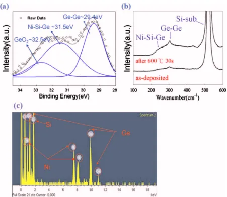
In order to confirm the attribution of the Ge elements during the NC formation process, the related material analy-ses was used. In the result of Ge 3d XPS analysis, a binding energy is found at ⬃31.5 eV, reported by the previous lit-erature indicated as nickel germane silicide 共Ni–Si–Ge兲 binding12 Additionally, the appearance of peak at 29.4 eV means the precipitation of the Ge. Figure2共b兲is the Raman spectra of the annealed NiSiGe samples. It can be seen that for the annealed NiSiGe film, there is a broad peak at about 220 cm−1, corresponding to the Ni–Si–Ge phase. Whereas a
Ge–Ge peak peaks at about 300 cm−1was found at 600 ° C thermal annealed samples.13Also, the EDS analysis was used to analyze the compositions of the NCs. The electron beam was focused at the NCs region about 10 nm during the EDS analysis. We found that the NCs composed with Ni, Si, and Ge elements. Through the results of the material analyses, it is believed that the main composition of the NCs is not pure NiSi2because the Ge can be the initial nucleation centers to form the NCs. According the reported literature, the Ge ele-ments tend to precipitate during the thermal annealing.14 Compared with the NiSi mixed film, the NiSiGe layer offers more additional nucleation centers for the NC formation. Therefore, the NiSiGe film can provide a more complete nucleation process and induce a higher size and density dis-tribution even at lower fabricating temperature.
Figure 3 shows the C-V hysteresis after bidirectional sweeps, which implies electron charging and discharging ef-fect of the MOIOS structure. In Fig. 3共a兲, the conventional NiSi NC memory device shows flatband voltage 共VFB兲 shift
of 4.5 V under ⫾10 V gate voltage operation. In contrast to the NiSi NCs, the NiSiGe NC memory device exhibits 9 V flatband voltage shift in Fig. 3共b兲. The larger window of NiSiGe NCs due to the improved NCs formation is advan-tage to be defined as “1” or “0” for the logic-circuit design.
FIG. 2. 共Color online兲 共a兲 The Ge 3d XPS spectra, 共b兲 Raman spectroscopy, and共c兲 EDS of the NiSiGe film after the thermal annealing.
FIG. 3. High-frequency共1 MHz兲 C-V characteristics of the MOIOS struc-tures: 共a兲 with NiSi NCs and 共b兲 NiSiGe NCs as the trapping layer of the memory device.
062102-2 Hu et al. Appl. Phys. Lett. 94, 062102共2009兲
This article is copyrighted as indicated in the article. Reuse of AIP content is subject to the terms at: http://scitation.aip.org/termsconditions. Downloaded to IP: 140.113.38.11 On: Wed, 30 Apr 2014 15:30:05
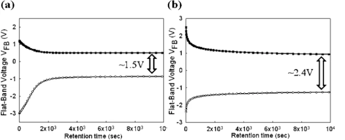
Figure 4 shows the retention characteristic of 共a兲 NiSi NC and 共b兲 NiSiGe NC devices. It is found that the NiSiGe NC device reveals better charge-storage ability than the NiSi NCs after 104 s. The better retention characteristic is
be-cause the NiSiGe NCs have lower quantum confinement ef-fect due to the larger NC size distribution.15Also, it is con-firmed the Ge elements of the NiSiGe film did not damage the tunneling oxide quality.16
In conclusion, we demonstrate the NiSiGe NCs memory device formed by annealing the NiSiGe film. It is confirmed the Ge element of NiSiGe film can offer more nucleation centers and enhance the NiSiGe NCs formation by the re-lated material analyses. Evan at lower annealing temperature, the NiSiGe film obtains larger NC size and higher density distribution. Furthermore, the NiSiGe NC memory device shows superior charge-storage ability to the conventional NiSi NCs due to the improved NC formation process. The good retention characteristic of NiSiGe NCs device is also advantageous to apply into the current memory fabricating process.
This work was performed at National Nano Device Laboratory and was supported by the National Science Council of the Republic of China under Contract Nos. NSC 2112-M-110-009, NSC 2221-E-009-151, NSC 97-2221-E-009-148, and NSC 97-3114-M-110-001.
1C. Y. Lu, T. C. Lu, and R. Liu, Proceedings of 13th IPFA共IEEE, New York, 2006兲, pp. 18–23.
2J. De Blauwe, IEEE Trans. Nanotechnol. 1, 72共2002兲.
3C. H. Lee, S. H. Hur, Y. C. Shin, J. H. Choi, D. G. Park, and K. Kim, Appl. Phys. Lett. 86, 152908共2005兲.
4S. Tiwari, F. Rana, K. Chan, H. Hanafi, C. Wei, and D. Buchanan, Tech. Dig. - Int. Electron Devices Meet. 1995, 521.
5T. Morimoto, T. Ohguro, H. S. Momose, T. Iinuma, I. Kunishima, K. Suguro, I. Katakabe, H. Nakajima, M. Tsuchiaki, M. Ono, Y. Katsumata, and H. Iwai,IEEE Trans. Electron Devices 42, 915共1995兲.
6P. X. Xu, S. R. Das, J. P. McCaffrey, C. J. Peters, and L. E. Erickson, Mater. Res. Soc. Symp. Proc. 402, 59共1995兲.
7J. D. Carey, L. L. Ong, and S. R. P. Silva,Nanotechnology 14, 1223 共2003兲.
8Y. Q. Wang, J. H. Chen, W. J. Yoo, Y. C. Yeo, S. J. Kim, D. L. Kwong, A. Y. Du, and N. Balasubramanian,Appl. Phys. Lett. 84, 5407共2004兲.
9D. Aurongzeb, S. Patibandla, M. Holtz, and H. Temkin,Appl. Phys. Lett.
86, 103107共2005兲.
10H. G. Chew, W. K. Choi, Y. L. Foo, F. Zheng, W. K. Chim, Z. J. Voon, K. C. Seow, E. A. Fitzgerald, and D. M. Y. Lai,Nanotechnology 17, 1964
共2006兲.
11L. Bi, Y. He, J. Y. Feng, and Z. J. Zhang, Nanotechnology 17, 2289 共2006兲.
12S. K. Ray, T. N. Adam, G. S. Kar, C. P. Swann, and J. Kolodzey, Mater. Res. Soc. Symp. Proc. 745, N6.6.1共2003兲.
13K. L. Pey, W. K. Choi, S. Chattopadhyay, H. B. Zhao, E. A. Fitzgerald, D. A. Antoniadis, and P. S. Lee,J. Vac. Sci. Technol. A 20, 1903共2002兲.
14W. K. Choi, V. Ng, S. P. Ng, H. H. Thio, Z. X. Shen, and W. S. Li,J. Appl. Phys. 86, 1398共1999兲.
15M. She and T. J. King,IEEE Trans. Electron Devices 50, 1934共2003兲. 16T. H. Ng, W. K. Chim, W. K. Choi, V. Ho, L. W. Teo, A. Y. Du, and C. H.
Tung,Appl. Phys. Lett. 84, 4385共2004兲.
FIG. 4. Retention characteristic of the 共a兲 NiSi and 共b兲 NiSiGe NCs memory device.
062102-3 Hu et al. Appl. Phys. Lett. 94, 062102共2009兲
This article is copyrighted as indicated in the article. Reuse of AIP content is subject to the terms at: http://scitation.aip.org/termsconditions. Downloaded to IP: 140.113.38.11 On: Wed, 30 Apr 2014 15:30:05