Very High Density RF MIM Capacitor Compatible with VLSI
K. C. Chiang
1, C. H. Lai
1, Albert Chin
2,*, H. L. Kao
1, S. P. McAlister
3and C. C. Chi
41
Nano Sci. Tech. Center, Dept. of Electronics Eng., Nat’l Chiao-Tung Univ., University System of Taiwan,
Hsinchu, Taiwan, ROC
2
SNDL, Dept. of Electrical & Computer Eng., National University of Singapore, Singapore 119260
*
on leave from
Nano Science Tech. Center, Univ. System of Taiwan- NCTU
[email protected]
3National Research Council of Canada, Ottawa, Canada
4
Dept. of Physics, National Tsing Hua Univ., Hsinchu, Taiwan, ROC
Abstract — We have fabricated RF MIM capacitors, using high-κ TiTaO as the dielectric, which show a record high density of 20 fF/µm2. In addition, the capacitors display a small capacitance reduction of only 3.6% over the 100 kHz to 20 GHz range, a low leakage current of 8 pA and a high Q of 120. This was for a typical large 8 pF TiTaO MIM capacitor. The small voltage dependence of the capacitance (∆C/C) of 770 ppm at 2 GHz, shows that these MIM capacitors are useful for high-precision RF circuits.
Index Terms — RF, capacitor, MIM, TiTaO. I. INTRODUCTION
To scale down the die size and cost of a RF IC, the areas of both the active and passive devices need to be reduced. Although the area of MOSFETs scale down by ~50% every 18-24 months, the passive RF devices do so at a much slower rate and occupy an increasing percentage of the IC area. Of all the passive devices the RF MIM capacitors [1]-[3] are the most frequently needed in an RF IC, being used for impedance matching, DC blocking and filtering. Therefore, to reduce the chip size and its cost, scaling down the MIM capacitor area is necessary. The practical way of achieving this is to increase the capacitance density (ε0κ/td) by using a high-κ dielectric
[4]-[7]. Decreasing the dielectric thickness (td) increases the
leakage current, loss tangent and the voltage dependence of capacitance (∆C/C), all of which is undesirable. The planned approach is to evolve the high-κ dielectric in RF MIM capacitors from SiON (κ~4-7) to Al2O3 (κ=10) to HfO2 (κ~22) or Ta2O5 (κ~25), according to the International Technology Roadmap for Semiconductors (ITRS). However, no practical high-κ dielectric for RF MIM capacitors has a κ value above 25. This is because increasing the κ value decreases the stability of the high κ dielectric, leading to unacceptably high leakage current. For example, although TiO2 has a dielectric constant of ~ 80, TiO2 RF MIM capacitors suffer from intolerably high leakage current, after the 400oC annealing needed for VLSI back-end process integration [4]-[7].
In this paper we report on record high-density (20 fF/µm2) RF MIM capacitors, using TiTaO as the dielectric, where the TiTaO has a high-κ value of ~45, which is greater
than the κ=25 barrier mentioned above. The motivation for using TiTaO is to take advantage of the high-κ property of the TiO2 , but to reduce the DC leakage by using a mixed dielectric, similar to our previous AlTaO study [5]. We have obtained good RF performance, in terms of a small reduction (< 5%) in the capacitor value, in the range 100 KHz to 20 GHz. Furthermore, ∆C/C was 770 ppm (representing a quadratic voltage coefficient of only 130 ppm/V2) in the RF frequency regime. Since these devices are fully process-compatible with current VLSI lines, our approach can achieve a potential reduction of the RF capacitor area of ~20 X, compared with technology currently available in foundries.
II. EXPERIMENTAL PROCEDURE
A thick SiO2 isolation layer was deposited on standard Si wafers in a VLSI back-end process. The lower MIM capacitor electrode was then fabricated on the SiO2/Si substrates using a sputter-deposited TaN/Ta bi-layer and then patterning. The thick Ta in the bi-layer structure is needed to reduce the RF ohmic loss and the thin TaN acts as a barrier between the high-κ dielectric and the Ta electrode. Then a thin TixTa1-xO (x~0.6) dielectric layer was deposited on the lower TaN/Ta electrode, followed by a 400oC oxidation and annealing step. This 400oC low-temperature thermal cycle is necessary for VLSI backend process integration. For comparison, we also fabricated capacitors using only TiO2 as the dielectric. Finally, Al was deposited and patterned to form both the top capacitor electrode and for the RF transmission lines.
The fabricated RF MIM capacitors were characterized using an HP4284A precision LCR meter from 10 KHz to 1 MHz, and an HP8510C network analyzer was used to measure the S-parameters from 200 MHz to 20 GHz (followed by a standard de-embedding procedure from a dummy open device [8]-[9]). The series inductance was also de-embedded with a through transmission line. The RF frequency capacitance was extracted from the measured S-parameters using an equivalent circuit model [5]. The RF frequency ∆C/C and quadratic voltage coefficient were then calculated using circuit theory, from the measured S-parameter data.
III. RESULTS AND DISCUSSION A. Low frequencies characteristics
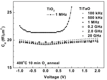
Fig.1 shows the C-V characteristics for TiO2 and TiTaO MIM capacitors, where record high capacitance densities of 21.5 and 20 fF/µm2 respectively, were found at 1 MHz. Current MIM capacitors provided by foundries have only ~1 fF/µm2. Hence the TiTaO capacitor provides a 20 times area reduction compared with current technology. The TiO2 MIM capacitor suffers from a large capacitance variation at voltages above 0.75 V. In contrast, constant capacitance values with little voltage and frequency dependence are shown by the TiTaO MIM capacitor – this is important for analog/RF circuit applications. TiTaO shows a high-κ value of ~45 – this is beyond the κ~22-25 range displayed by HfO2 and Ta2O5 , used in current DRAM manufacturing processes (Fig. 2).
-1.0 -0.5 0.0 0.5 1.0 1.5 2.0 15 20 25 TiO2 1 MHz TiTaO 100 kHz 500 kHz 1 MHz 0.2 GHz 2.0 GHz 20 GHz 400oC 10 min O 2 anneal CH (fF/ µ m 2 ) Voltage (V)
Fig.1 The C-V characteristics for TiO2 and TiTaO MIM
capacitors measured at different frequencies.
1 10 100 0 2 4 6 8 10 TiTaO Ta2O5 Al2O3 HfO2 Si3N4 TiO2 Bandgap ( eV)
κ
Value
SiO2 This workFig.2 The evolution of high-κ values for Analog/RF MIM and DRAM capacitors. TiTaO provides twice the κ value than HfO2.
To investigate the abnormal large capacitance variation in TiO2 capacitors at applied voltage > 0.75 V, we have
measured the DC Current-Density and Voltage (J-V) characteristics. As shown in Fig. 3, the TiO2 capacitor leakage
current increases rapidly with increasing voltage, giving rise to the abnormal capacitance increase in the C-V curve in Fig. 1. This large leakage current is related to the poly-crystallization of the TiO2 from its amorphous state, after the 400
o
C O2
annealing, which generates a high current conduction path through poly-grain boundaries. In contrast the TiTaO MIM capacitors provide ~ 6-7 orders of magnitude lower leakage current than do the TiO2 ones, and a low leakage current of
2.0×10⁻⁶
A/cm2
is measured at 1V. The leakage current for a capacitor (C) can be obtained from J×C/Cd, where J is shown in Fig. 3 and Cd is the capacitor density (20 fF/µm
2
) from Fig. 1. For the relatively large 8 pF capacitor used in this work, the leakage current is as low as 8 pA, due to the very small area with dimensions of 20 µm × 20 µm. 0 1 2 3 4 10-8 10-6 10-4 10-2 100 102 TiO2 TiTaO Curr ent Densi ty ( A /cm 2 ) Voltage (V)
Fig. 3. The J-V characteristics for TiO2 and TiTaO MIM capacitors, after the 400o
C O2 anneal for 10 min. The large leakage current in the TiO2 device is due to the formation of poly-crystalline grains. The leakage current is 6-7 orders of magnitude lower in the TiTaO MIM capacitors.
B. High frequencies characteristics
We have measured the S-parameters to investigate the RF frequency characteristics beyond the 1 MHz upper limit of precision LCR meter. Fig. 4 shows the S-parameters for a TiTaO MIM capacitor. The RF frequency capacitance can be extracted from the S-parameters using the equivalent-circuit model shown in Fig. 5 [6]. The C, RP, LS, and RS in this model
are the capacitor, parallel resistance, parasitic series inductance, and parasitic series resistance, respectively, where the RS and LS are from the connected transmission lines. The
extracted capacitor values, at different bias voltages and at RF frequencies of 0.2, 2.0 and 20 GHz, are also shown in Fig. 1.
0.5 1.0 2.0 5.0 -0.5j 0.5j -1.0j 1.0j -2.0j 2.0j -5.0j 5.0j open:S21 solid:S11
Fig. 4. The measured scattering parameters of a TiTaO MIM capacitor, from 200 MHz to 20 GHz.
R
PC
R
SL
S2L
S1Fig. 5. The equivalent-circuit model used for capacitance extraction from the measured S-parameters. The C and RP are the
capacitor and its parallel resistance, and the LS and RS are the
parasitic inductance and resistance, obtained from transmission lines connected between the capacitor body and probing pads.
The frequency dependence of the capacitance is shown in Fig. 6. Only a small variation of 3.6% occurs over the frequency range up to 20 GHz. In addition, a high quality (Q) factor of ~120 is shown at 1 GHz for an 8 pF capacitor. The nearly constant capacitance values, as shown in Fig. 6, in combination with the high Q-factor are important for analog/RF ICs incorporating such high density capacitors and operating from the IF to the RF regime.
The variation of capacitance (∆C/C), is one of the most important parameters for analog/RF IC applications. The value
of ∆C/C below 1 MHz can be calculated from the C values,
shown in Fig. 1 and measured by a precision LCR meter. However, the accuracy of ∆C/C at RF frequencies is insufficient if obtained from the equivalent-circuit model. To achieve high precision ∆C/C at the RF frequencies, we used equation (1), previously derived [5] for this purpose:
) ( ) / 1 ( 2 ] / ) ( 2 [ 21 2 2 2 0 0 j C R j C S R Z Z Z C C p P ∆ + + = ∆ ω ω ω (1) 10-5 10-4 10-3 10-2 10-1 100 101 102 18 19 20 21 22 C a pacitance ( fF/ µ m 2 ) Frequency (GHz)
Fig. 6. The frequency-dependence of the capacitance for a TiTaO MIM capacitor. The capacitance reduction is only observed at low frequency, since the trapped carriers in the high-κ dielectric of MIM capacitor can not follow the high frequency signal.
Z(ω) in equation (1) is the total frequency-dependent impedance between the two ports with Z0 being the characteristic impedance of the transmission line. Based on the circuit theory derived equation (1), the ∆C/C can be obtained by differentiating the measured S21, i.e., ∆S21 to enhance the small variations from the S-parameters. The RF frequency ∆C/C is plotted in Fig. 7. The ∆C/C data below 1 MHz, measured using the precision LCR meter, is also plotted for comparison. A rapid decrease of ∆C/C is observed with increasing frequency in the range 1 MHz to 200 MHz.
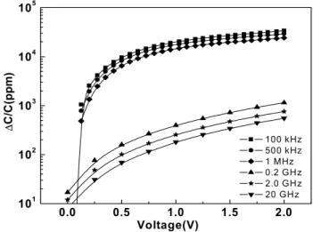
0.0 0.5 1.0 1.5 2.0 101 102 103 104 105 100 kHz 500 kHz 1 MHz 0.2 GHz 2.0 GHz 20 GHz Voltage(V) ∆ C/C (ppm)
Fig. 7. The voltage dependence of the capacitance (∆C/C) for a
TiTaO MIM capacitor. The low frequency data ≤ 1 MHz is from the
C-V measurements in Fig. 1, and the RF frequency data >0.1 GHz is
derived by eq. (1) from measured S-parameters.
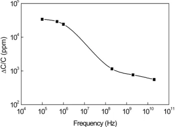
To demonstrate the frequency dependence, we plot ∆C/C from 100 kHz to 20 GHz, in Fig. 8. Most of the decrease of
∆C/C with increasing frequency occurs in the 1 MHz to 200
MHz range. Because the typical carrier lifetime from
related Shockley-Read-Hall (SHR) recombination is in the order of ~µs, the reduction of ∆C/C within the 1MHz to 200 MHz range may be due to the trapped carriers being unable to follow the high frequency signal [10]-[12]. The observed small ∆C/C of 770 ppm at 2GHz, or equivalent to a low quadratic voltage coefficient α of 130 ppm/V2, is sufficient to meet the tight requirements of high-speed analog/RF IC applications. 104 105 106 107 108 109 1010 1011 102 103 104 105 ∆ C/C ( p pm ) Frequency (Hz)
Fig. 8. ∆C/C for a 20 fF/µm2 TiTaO MIM capacitor, biased at 2V,
as a function of frequency. The line was drawn by hand and guided by the eye.
IV.CONCLUSIONS
We have demonstrated TiTaO MIM capacitors that have a high capacitance density of 20 fF/µm2, a small capacitance reduction of 3.6%, and small ∆C/C of 770 ppm at 2 GHz. The good MIM capacitor integrity makes them suitable for precision circuit applications at RF frequencies.
ACKNOWLEDGEMENT
We would like to thank G. W. Huang at the National Nano-Device Lab. for help with the RF measurements. This work was supported by the joint project of NRC-Canada and NSC-Taiwan ROC.
REFERENCES
[1] Z. Chen, L. Guo, M. Yu, and Y. Zhang, “A study of MIMIM on-chip capacitor using Cu/SiO2 interconnect technology,”
IEEE Microwave and Wireless Components Lett., vol. 12, pp.
246-248, July 2002.
[2] C. P. Yue and S. S. Wong, “A study on substrate effects of silicon-based RF passive components,” IEEE MTT-S Int.
Microwave Symp. Dig., pp. 1625-1628, June 1999.
[3] C.-M. Hung, Y.-C. Ho, I.-C. Wu, and K. O, “High-Q capacitors implemented in a CMOS process for low-power wireless applications,” IEEE MTT-S Int. Microwave Symp. Dig., pp. 505-511, June 1998.
[4] C. H. Lai, C. F. Lee, A. Chin, C. H. Wu, C. Zhu, M. F. Li, S. P. McAlister, and D. L. Kwong, “A tunable and program-erasable capacitor on Si with long tuning memory,” IEEE RF IC Symp.
Dig., pp. 259-262, June 2004.
[5] C. H. Huang, M.Y. Yang, A. Chin, C. X. Zhu, M. F. Li, and D. L. Kwong, “High density RF MIM capacitors using high-κ AlTaOx dielectrics,” IEEE MTT-S Int. Microwave Symp. Dig., vol. 1, pp. 507-510, June 2003.
[6] S. B. Chen, J. H. Chou, A. Chin, J. C. Hsieh, and J. Liu, “RF MIM capacitors using high-κ Al2O3 and AlTiOx dielectrics,”
IEEE MTT-S Int. Microwave Symp. Dig., vol. 1, pp. 201-204,
June 2002.
[7] C. Zhu, H. Hu, X. Yu, S. J. Kim, A. Chin, M. F. Li, B. J. Cho, and D. L. Kwong, “Voltage temperature dependence of capacitance of high-K HfO2 MIM capacitors: A unified understanding and prediction,” Int. Electron Devices Meeting
(IEDM) Tech. Dig., pp. 379-382, Dec. 2003.
[8] M. C. King, M. T. Yang, C. W. Kuo, Y. Chang, and A. Chin, “RF noise scaling trend of MOSFETs from 0.5 µm to 0.13 µm technology nodes,” IEEE MTT-S Int. Microwave Symp. Dig., vol. 1, pp. 9-12, June 2004.
[9] M.C. King, Z. M. Lai, C. H. Huang, C. F. Lee, M. W. Ma, C. M. Huang, Y. Chang and Albert Chin, “Modeling finger number dependence on RF noise to 10 GHz in 0.13 µm node MOSFETs with 80nm gate length,” IEEE RF IC Symp. Dig., pp. 171-174, June 2004.
[10] K. T. Chan, A. Chin, S. P. McAlister, C. Y. Chang, V. Liang, J. K. Chen, S. C. Chien, D. S. Duh, and W. J. Lin, “Low RF loss and noise of transmission lines on Si substrates using an improved ion implantation process,” IEEE MTT-S Int.
Microwave Symp. Dig., vol. 2, pp. 963-966, June 2003.
[11] A. Chin, K. T. Chan, H. C. Huang, C. Chen, V. Liang, J. K. Chen, S. C. Chien, S. W. Sun, D. S. Duh, W. J. Lin, C. Zhu, M.-F. Li, S. P. McAlister and D. L. Kwong, “RF passive devices on Si with excellent performance close to ideal devices designed by electro-magnetic simulation,” Int. Electron
Devices Meeting (IEDM) Tech. Dig., pp. 375-378, Dec. 2003.
[12] K. T. Chan, A. Chin, C. M. Kwei, D. T. Shien, and W. J. Lin “Transmission line noise from standard and proton-implanted Si,” IEEE MTT-S Int. Microwave Symp. Dig., vol. 2, pp. 763-766, June 2001.