Vertical integration of a GaAsIAIGaAs
quantum-well infra-red photodetector
J.S. Tsang, C.P. Lee, K.L. Tsai and
H.R.Chen
-__--A---_-_-
II I---.. ---I I--- .-...-l--&Lquariruiri-weii iaser aiiu a i ~ i i y - ~ a ~ ~ ~ e i i y ~ i i
Indexing terms: Integroted optoelectronics, Semiconductor Lasers, Infrored detectors, Photodetectors
A short-wavelength (-0.8pn) GaAy'AIGaAs graded-index separateconfmement heterostructnre quantum-well laser has been monolithidly integrated with a long-wavelength (-8pm) GaAs/
AlGaAs multiplequantum-well infra-red photodetector on a semi-insulating G a A s substrate by molecular beam epitaxy. The vertical integration method is used and the combined strncture is a pinin smctnre. Both the laser and detector exhibit excellent characteristics. At room temperature, the ridge waveguide laser has an extremely low threshold current of 2SmA and a diEerential quantum efficiency above 65% with a stripe width of 20pn. The quantum-well detector has a peak response at 8~ and a responsivity of 0.7AM'.
In recent years there has been continuous interest in developing optoelectronic integrated circuits (OEICs). This is mainly due to the potential for achieving compact, highly-reliable and multifunc- tional devices. To integrate different functional devices, the com- patibilities of the materials used and the device structures must be considered. Among the various integration techniques, the vertical integration method which stacks two structures one on top of the other is one of the simplest [I, 21. It does not require the regrowth process which often degrades the quality of the epitaxial layers and has been applied in the integration of a laser with a hetero- junction bipolar transistor, a laser with a field-effect transistor and a laser with a photodetectors 1 2 4 . In previously reported work, the laser and the photodetector integrated as an optoelectronic device are often operates at the same wavelengths [5, 61. In this Letter we demonstrate for the fust time the integration of a short- wavelength ( - 0 . 8 ~ ) near-infra-red laser and a long wavelength (-8pm) quatum-well infra-red photodetector (QWIP). This inte- grated device, for future application, can be used to convert a far- infra-red signal to a near-infra-red (or visible) light signal. The device, which includes a ridge-waveguide laser and a grating-cou- pled QWIP, is fabricated on a semi-insulating substrate with all the contact electrodes on the front surface.
n -AIosG%4A~
5 I
-
GaAs ~ s l r o l e m Fig. 1 Schematic structure of vertical integrated deviceThe schematic structure of the integrated device is shown in Fig. 1. The integrated structure contains a graded-index separatecon- finement heterostructure (GRINSCH) laser and a quantum-well infra-red photodetector (QWIP). The epilayers were grown by a Varian GEN-I1 molecular-heam-epitaxy (MBE) system on a (100) semi-insulating GaAs substrate. The first stacked structure was designed as an nin QWIP structure. It consisted of a 1 . 4 ~ - t h i c k n+-GaAs bottomcontact layer (Si = 2 x 10¹⁸cn-3), 20-period GaAdAlGaAs quantum wells with each period consisting of a 40A n-GaAs quantum well (Si = 1 x 10'8cn-3) sandwiched between 400A undoped A&.,Gh,,As bamers, and a 1.1m-thick n+-GaAs top contact layer (Si = 2 x 10¹⁸cn-3). The top contact layer of the QWIP was also used as the n-type contact layer of the integrated laser. Then, the layers for the laser were grown on top of the n+-GaAs top contact layer. It consisted of a 1.0pm-thick n+- Al,,,G~,,As cladding layer (Si = 1 x 10¹⁸cn-3), a 0.15pm-thick
undoped Al,Ga,&s graded-index layer (x = 0.64.2), a 65A index layer (x = 0.2-0.6), a 1.0pm-thick p-&,Gh,As cladding layer (Be = 1 x 10¹⁸m-3), a 0 . 1 5 ~ p-Al,Ga,&s graded-index layer (x=0.6-0.2), and a 0.3pmpt-GaAs ohmic contact layer (Be = 2 x 10¹⁸cn-3). The whole structure was grown at 580°C with an
& source. After MBE growth, the ridge-waveguide pattern was obtained by standard photolithography and wet chemical etching. The width of the stripe was 20pm and the etched depth was about 1 . 2 ~ . After chemical etching, a l5WA S O , layer was deposited by plasmaenhanced chemical vapour deposition. Contact win- dows were opened and AuBe was deposited as the p-type contact. After ptype metallisation, another photolithography step was per- formed to protect the laser stripe region, and the area not pro- tected was etched away to expose the n+-GaAs top contact layer of the QWIP. After wet etching, AuGe was deposited and used as the n-type contact of the laser. Then, 3 p n etched stripe gratings which were used to couple the nonnal incident infra-red radiation were fabricated on the n'GaAs top contact layer by standard photoli- thography and wet chemical etching. Then another chemical etch- ing step was performed to expose the bottom GaAs layer and AuGe was deposited as the bottom electrode of the QWIP. The substrate was then lapped down to 100pm; devices with a cavity length of 400 pn and a width of 6OOpm were obtained by cleav- ing. The widths of all the contact regions were 1 0 0 ~ and the width of the stripe grating region was 2 0 0 ~ .
After the fabrication process, the lasers were measured at room temperature under pulse conditions. The QWIPs were measured with infra-red irradiation from the front side at 77K by the Nicolet Fourier transform infra-red spectrometer. The responsivity of the detector was measured by the standard lock-in technique using a 973K black-body source.
Cm-A2 p ~ t
=e.-,
iI ~e,
~ 5 ~ ~ - t h i ~ ~ i&mi@- AJxChP4s -rn-dd-3 p51121
injection current.mA
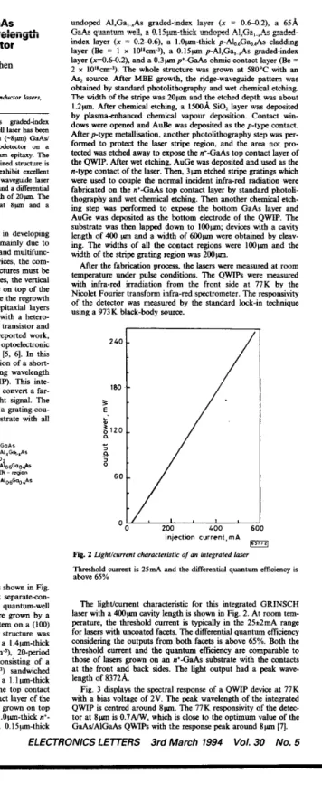
Fig. 2 Light/currmt characterisric of an inregrared h e r Threshold current
above 65% is 25mA and the differential quantum efficiency is
The light/current characteristic for this integated GRINSCH laser with a 4 0 0 ~ cavity length is shown in Fig. 2. At room tem- perature, the threshold current is typically in the 25*2mA range for lasers with uncoated facets. The differential quantum efficiency considering the outputs from both facets is above 65%. Both the threshold current and the quantum efficiency are comparable to those of lasers grown on an n+-GaAs substrate with the contacts at the front and back sides. The light output had a peak wave- length of 8372A.
Fig. 3 displays the spectral response of a QWIP device at 77K with a bias voltage of 2V. The peak wavelength of the integrated QWIP is centred around 8pm. The 77K responsivity of the detec- tor at 8pm is 0.7A/W, which is close to the optimum value of the GaAdAlGaAs QWIPs with the response peak around 8 p
[q.
6 8 10 12 1sTiTjl wavelength ,vm
Fig. 3 Spectral response of integrated Q WIP with bias voltage of 2 V a t 77K
In conclusion, we have successfully used the vertical integration method to integrate a GaAdAlGaAs GRINSCH quantum-well laser and a GaAdAIGaAs long-wavelength photodetector by molecular beam epitaxy. The laser’s emission wavelength and the photodetector’s absorbtion wavelength fall in the near-infra-red and far-infra-red, respectively. The peak wavelength of the laser spectrum is 8372A at room temperature and the response peak of the QWIP is centred around 8 p at 77K. The typical laser’s threshold current is 25mA and the differential quantum efficiency is above 65%. The responsivity of the detector is about 0 . 7 M at 8W.
Acknowledgment: We would like to thank L. J. Cheng for device bonding. This work was supported in part by the National Science Council of the Republic of China under contract NSC82-0404- EOO9-381.
6 IEE 1994
Electronics Letters Online No: 19940295
J. S . Tsang, C. P. Lee, K. L. Tsai and H. R. Chen (Department of Electronics Engineering and Institute of Electronics, Natwnal Chiao Tung University, Hsin-Chu, 3W50, Taiwan, Republic of China)
7 January 1994
Ref-
1 HONDA, Y., SUEMUNE, I., YASUHIRA. N., and YAMANISHI, M : ‘A new optoelectronic device based on modulation-doped heterostructure: Demonstration of functions as both lateral current injection laser and junction field effect transistor’, IEEE Photonics. Technol. Lett.,
1990, 12, pp. 881483
vertical monolithical combination of an InGaAsPflnP laser and a heterojunction bipolar transistor’, IEEE J. Quantum Electron..
1987, QED, pp. 919-924
and EASTMAN, L.F.: ‘Vertical integration of an In, ,sG%.8& modulation doped field effect transistor and GaAs laser grown by molecular beam epitaxy’, Electron. Lett., 1990, 26, pp. 350-351 D ~ AN.K., , and CHO. A.Y.: ‘Monolithic integration of photodetector with vertical cavity surface emitting laser’, Electron. Lett., 1991, 27, pp. 1630-1631
YARIV, A.: ‘Mhh lasers with microcleaved mirrors suitable for monolithic integration’, Appl. Phys. L e f t . , 1982, 40, pp. 289-291
6 NOBUHARA, H., WADA, o., and Fum, T.: ‘GRINSCH SQW laser/ photodiode array by improved microcleaved facet process’,
Electron. Lett., 1985, 21, pp. 718-719
,
1
2 CHEN, T.R., UT= K., ZHUANG, Y H., LIU, Y.Y., and VARIV, A.: ‘A
i
3 OFFSEV, S.D., TASKER,P.J., SCHAFF, W.I., KAPITAN, L., SHEALY,J.R.,
I 4 HASNAIN,G., TALK., WANG,Y.H., WYNN,J.D., CHOQUETIZ,K.D., ~
i
5 BLAWELT, H., BAR-CHAIM,N., FEKETE, D., MARGALIT,S., and
ELECTRONICS LEl7ERS
3rdMarch
1994Vol.
30
7 TSAI,K.L., CHANG. K.H., LEE,C.P., HUANG, K.F, TSANG, IS., and and strained InGaAdAIGaAs multiquantum wells’, Appl. Phys. Lett., 1993, 62, pp. 35W3506
CUEX, U,%.: ‘TW -!er ‘-f-:ed phe:--’e:Ekx .:sizg G&’A!G?,
Effective boundary of channel in quasi-two-
dimensional simulation of thin-film
semiconductor devices
A.A. Barybin and
V.V. PerepelovskiIndexing t e r n : Semiconductor device models, MESFETs, Thin
jih transistors
An effective boundary between current channels and depletion regions is introduced. The position of this boundary is defined by taking account of the carrier diiliiion in the current channel. This gives a correction to the potential determining the depth of depletion without a diffused channel houndq.
Introduction: The quasi-two-dimensional models of MESFETs [l, 21 are based on the assumption of an abrupt boundary between the current channel and depletion region. Quasi-two-diiensional models (QTDMs) have been created with a transition layer between the depletion region and channel [3]. However, the pro- posed methods allowing for distribution of charge carriers in the transition layer are somewhat artificial. Below, the problem of modelling MESFET-type structures with smooth boundaries between the depletion region and the channel is reduced to an abrupt boundary problem. This will allow use of QTDM equa- tions obtained formerly while assuming a boundary to be abrupt.
I a t e I z
Fig. 1 Effective boundary of channel-depletion region
Physical model: The results of MESFET two-dimensional simula- tion having been analysed, it is possible to use the Boltzmann dis- tribution for free charge carriers in a t h i n - f h semiconductor structure (J’FSS) in transverse directions, particularly along the y- axis in Fig. 1 (the z-axis is directed from source to drain):
n ( y , z ) = $z)exp{-‘~pT’[ip(y.z) - S(z)l) ‘PT = kTJq (1) Here [‘pcyIz) -
p(z)]
is a distribution of the potential in the-TFSS cross-section relative to the mean channel potential @(z), n ( z ) isthe mean carrier concentration in the channel, and T.(z) is the electron temperature. The mean values (p(z), n ( z ) etc. are given by averaging over the channel cross-section. We introduce the effec- tive boundary D(z) of a channel by means of the following equal- ity (see Fig. 1):
H
d Y ,
Z)V(Y, 2) dY =w
J
qP(z) - “(Y, Z)lV(Y,Z) dY D(2) where H is the TFSS total thickness, W is the TFSS width along the x-axis, and *,z) is the electron velocity. The left-hand side of eqn. 2 equals the current flowing in the region confined by the gate (at y = 0) and the introduced effective boundary (at y = 0).
This region is denoted by I in Fig. 1. The right-hand side of eqn. 2 corresponds to the region I1 in Fig. 1 and is written down pro- ceeding from the fact that the current in this region is equivalent