Periodically Lateral Silicon Grains Fabricated by Excimer
Laser Irradiation with a-Si Spacers for LTPS TFTs
Huang-Chung Cheng,a Chun-Chien Tsai,a,z Jian-Hao Lu,a Hsu-Hsin Chen,a Bo-Ting Chen,aTing-Kuo Chang,band Ching-Wei Linb
a
Department of Electronics Engineering and Institute of Electronics, National Chiao Tung University, Hsinchu, Taiwan
b
Toppoly Optoelectronics Corporation, Miao-Li County, Taiwan
Low-temperature polycrystalline silicon共LTPS兲 thin-film transistors 共TFTs兲 with a periodic lateral silicon grain structure have been demonstrated to exhibit high-performance electrical characteristics via the amorphous silicon spacers above the amorphous silicon film crystallized with excimer laser. Amorphous silicon spacers allowed the bottom of the under-layered amorphous silicon film to serve as seed crystals. The periodic grain structure could be artificially controlled via the super lateral growth phenomenon during excimer laser irradiation. Consequently, such periodically large and lateral grains in the TFTs would achieve high field-effect-mobility of 298 cm2/V s, as compared with the conventional ones of 128 cm2/V s. In addition, the uniformity of device-to-device could be improved due to this location-manipulated lateral silicon grains.
© 2006 The Electrochemical Society. 关DOI: 10.1149/1.2382420兴 All rights reserved.
Manuscript submitted June 19, 2006; revised manuscript received August 22, 2006. Available electronically November 8, 2006.
Low-temperature polycrystalline silicon共LTPS兲 thin-film transis-tors fabricated by excimer laser crystallization 共ELC兲 have been extensively studied for active matrix liquid crystal displays 共AML-CDs兲 and active matrix organic light emitting displays 共AMOLEDs兲 owing to their high driving-current capability.1,2 Although field-effect-mobility of 200 cm2/V s for TFTs has been attained by ELC, it is difficult to make the laser energy density hit the super lateral growth regime everywhere due to the fluctuation of pulse-to-pulse energy and amorphous silicon 共a-Si兲 layer thickness.3-5 Further-more, in the applications of system-on-panel 共SOP兲, high-performance LTPS TFTs are still needed to integrate memory and controller with driver circuits on a single substrate. Thus, there is a great interest in improving the performance of LTPS TFTs by laser crystallization approaches, including sequential lateral solidification by laser beam scanning within several micrometers step by step,6-9 phase-modulated ELC using an optical phase-shift mask,10-12 -Czochralski 共grain filters兲 method,13-15
ELC of selectively floating a-Si layer,16,17CLC method using the diode-pumped solid state con-tinuous wave laser,18,19and selectively enlarging laser crystallization 共SELAX兲.20However, most of them are complicated or not easy to control from the viewpoints of LTPS TFTs fabrication.
In this work, a novel crystallization process for producing high-mobility poly-Si TFTs is proposed. Periodically lateral silicon grains with 2m in length can be artificially grown in the channel regions via the amorphous silicon spacer structure with excimer laser irra-diation. It leads to the enhancement of device performance and the improvement of device uniformity. The effect of the number of grain boundary on large dimension TFTs is also investigated.
Experimental
The maximum process temperature of n-channel LTPS TFTs fab-rication is 550°C for the deposition of a-Si thin films with low-pressure chemical vapor deposition共LPCVD兲. Figure 1 illustrates the key processes for the fabrication of LTPS TFTs crystallized with a-Si spacer structure. At first, a 1000 Å thick amorphous silicon 共a-Si兲 layer was deposited by pyrolysis of pure silane 共SiH4兲 by LPCVD at 550°C on oxidized silicon wafer with oxide thickness of 1m. Then, a 500 Å thick tetraethyl orthosilicate 共TEOS兲 oxide layer was deposited by plasma-enhanced chemical vapor deposition 共PECVD兲 at 385°C. Next, the TEOS oxide layer in some regions was removed to form individual islands following by another 1000 Å thick a-Si layer deposition by LPCVD at 550°C. Subse-quently, the upper a-Si layer was etched by transformer-coupled plasma reactive ion etching共TCP-RIE兲 to leave the a-Si spacer on
the initial a-Si thin film. After stripping-off the remains of TEOS oxide by buffer oxide etchant共BOE兲, excimer laser crystallization 共ELC兲 was performed by KrF excimer laser 共 = 248 nm兲. During the laser irradiation, the samples were located on a substrate in a vacuum chamber pumped down to 10−3Torr and substrate was maintained at 400°C. The number of laser shots per area was 20 共i.e., 95% overlapping兲 and laser energy density was varied. After defining the device active region, a 1000 Å thick TEOS gate oxide was deposited by PECVD at 385°C. Then, a 2000 Å thick a-Si thin film was then deposited by LPCVD at 550°C for gate electrode. The a-Si thin film and gate oxide were etched by TCP-RIE to form the gate electrode. A self-aligned phosphorous ion implantation with dose of 5⫻ 1015cm−2 was carried out to form source and drain regions. Next, a 3000 Å thick TEOS passivation oxide was depos-ited and the implanted dopants were activated by thermal annealing at 600°C for 12 h. Finally, contact holes opening and metallization were carried out to complete the fabrication of TFTs with spacer structure. No hydrogenation plasma treatment was performed during the device fabrication process. For the sake of comparison, the con-ventional excimer-laser-crystallized LTPS TFTs with a channel thickness of 1000 Å were also fabricated.
Results and Discussion
Atomic force microscopy共AFM兲 analysis is used to investigate the surface morphology of silicon thin film before and after laser crystallization. Figure 2a and b display the AFM images of silicon thin film with 1500 Å thick spacer height before and after excimer laser irradiation, respectively. Three apparent silicon spacer lines are indicated by white dashed lines formed using dry-etching of the a -Si/TEOS-SiO2step structure following the TEOS stripping-off be-fore laser irradiation in Fig. 2a. After laser crystallization, the spac-ers disappear and the silicon thin film becomes smooth due to the effect of surface tension during excimer laser irradiation. The loca-tion of a-Si spacers has been verified by protecting some spacers from excimer laser crystallization. The ridge and hillock configura-tional occurs at the grain boundaries due to the freezing of capillary waves excited in the melting silicon during laser crystallization.21 Figure 3 shows the Raman spectra from poly-Si film with periodic lateral grains, from the conventional excimer-laser-crystallized poly-Si film, and from a silicon wafer for reference. The insets de-scribe that full width at half-maximum共fwhm兲 and normalized peak intensity of the poly-Si film with periodic lateral silicon grains 共PLSG兲 are close to those of silicon wafer, reflecting the fact that the crystallinity of PLSG poly-Si film is better than that of conventional ELC poly-Si film.
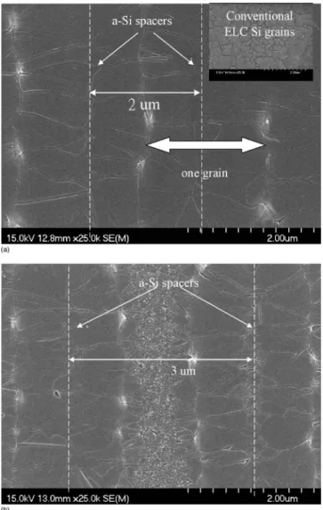
Figure 4a and b show the SEMs of excimer laser crystallized poly-Si with a-Si spacer structure after Secco etching and the
dis-z
tances between adjacent a-Si spacers are 2 and 3m, respectively. The inset in Fig. 4a shows the microstructure of conventional ELC poly-Si with the same scale. The location of a-Si spacer is indicated by white dash lines. It can be observed that Fig. 4a shows the trans-verse grains with 2m in length formed periodically in the laser crystallized poly-Si thin film, while small and fine grains which are present in Fig. 4b, are caused by spontaneous homogeneous nucle-ation. It has been reported that lateral thermal gradient could arise as a result of the heat generated at moving solid-melting interfaces.5,22 As a proper laser energy density is performed on the amorphous silicon thin film containing different thickness, the thin silicon re-gion is completely melted while the thick rere-gion is partially melted, and the lateral grain growth starts from the unmelted solid Si toward the completely melted thin region. In this experiment, as excimer
laser irradiation is performed on the amorphous silicon thin film with a-Si spacers, the laser energy densities can cause complete melting 1000 Å thick silicon thin film but partial melting 1500 Å thick a-Si film. Therefore, the 1000 Å thick poly-Si film with the 500 Å thick spacer will proceed the lateral grain growth starting from the unmelted silicon solid seed under the spacer, and extend toward the completely melted region until the solid-melt interface from opposite direction impinges. If the a-Si seeds were arranged in a proper distance, periodic grain growth will be manufactured with-out any spontaneous nucleation. Thus, the grain boundaries in the channel region can be controlled and reduced. From the SEM analy-ses, the maximum achievable length of lateral grain growth in this crystallization method is⬃2.5 m. Because the number of sponta-neous small grain and grain boundary is reduced, the uniformity of TFTs performance can be improved with artificially periodic lateral grains.
Typical transfer characteristics and output characteristics of LTPS TFTs with periodic lateral silicon grains and conventional ones for W = L = 2m are shown in Fig. 5a and b, respectively. Several important electrical characteristics of the TFTs are listed in Table I. The threshold voltage was defined as the gate voltage re-quired to achieve a normalized drain current of Ids=共W/L兲 ⫻ 10−8A at V
ds= 0.1 V. The field-effect-mobility and subthreshold swing were extracted at Vds= 0.1 V, and the Ion/Ioff current ratio was defined at Vds= 5 V. Owing to the uniformly large transverse grains grown in the device channel region, TFTs with periodic lat-eral grains exhibit better electrical characteristics than the conven-tional ones. Poly-Si TFT with field-effect-mobility of 298 cm2/V s can be achieved using this a-Si spacer crystallization method while the mobility of the conventional counterpart is⬃128 cm2/V s. It is generally believed that the grain boundary acts as a strong trapping center which degrades the performance of TFTs resulting from grain boundary potential barrier height. The high field-effect-mobility is attributed to that the carrier transport is not interrupted by the grain boundary parallel to the channel direction for the periodic lateral grain silicon structure. Although small and fine grains are located in the channel region as the distance between neighboring a-Si spacers exceeds 2.5m, the characteristics of TFTs crystallized with a-Si spacer structure are still better than those of conventional TFTs.
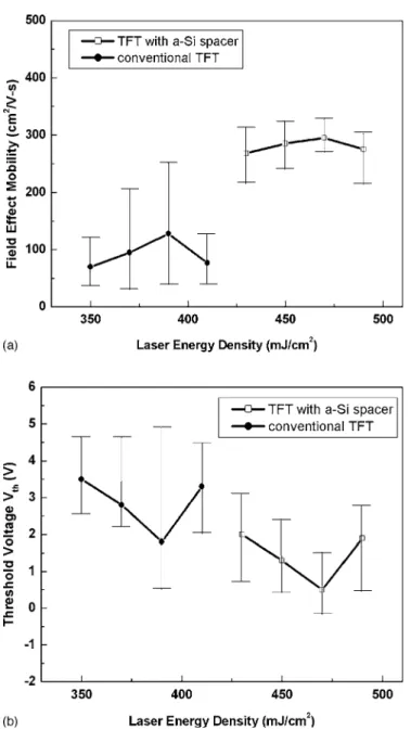
In addition to the improvement of LTPS TFTs performance, TFTs with periodic lateral grains demonstrate better uniformity due to the wide laser process window. Figures 6a and b show the dependences of field effect mobility and threshold voltage on laser energy densi-ties for LTPS TFTs crystallized with two different structures whose channel length is 2m. In Fig. 6a and b, twenty TFTs for each laser irradiation condition are measured to study the device-to-device variation. The vertical bars in the figures indicate the maximum and minimum characteristic values and the solid symbols are the average calculated characteristic values at the specific laser energy density. Unlike the conventional devices, it is found that the threshold volt-age and field-effect-mobility of LTPS TFTs with periodic lateral grains are much less sensitive for different laser energy densities.
Because periodic lateral silicon grains can be arranged periodi-cally inside the channel region共Fig. 4a兲, this proposed crystalliza-tion method is also suitable for large dimension TFTs. Figure 7 displays the schematic illustration of the positions of a-Si spacer in the channel region for large-sized device. Periodic lateral grains are constructed inside the channel and the number of longitudinal grain boundaries can be varied by adjusting the distance of adjacent a-Si spacers. Figure 8a and b show the typical transfer characteristics and output characteristics of LTPS TFT crystallized with periodic lateral silicon grains, in which the distance between neighboring a-Si spac-ers is 2.5m, and conventional one for W = L = 10 m, respec-tively. Table II summarizes several important electrical characteris-tics of the TFTs crystallized with conventional and a-Si spacer structures, in which the distances between adjacent spacers are 1, 2, 2.5, 3, and 4m, respectively. The device channel width and length are equal 10m. Periodic lateral grains in the channel region make Figure 1.共Color online兲 The key processes for fabricating small-dimension
LTPS TFTs with a-Si spacer structure.
J6 Journal of The Electrochemical Society, 154共1兲 J5-J10 共2007兲
the performance of poly-Si TFTs better than that of conventional TFTs. Besides the enhancement of field-effect-mobility, high on/off current ratio, and low threshold voltage are also demonstrated in these devices. These electrical characteristics are gradually im-proved due to the decrease of the number of longitudinal grain boundaries in the channel region as the distance between adjacent a-Si spacer increases. The optimal electrical characteristics are ob-tained when the distance between neighboring a-Si spacers is
2.5m. This result is consistent with the SEM analyses, which reveal that the largest lateral grain crystallized made by this tech-nique is⬃2.5 m.
Conclusions
A new crystallization technology for producing periodic lateral silicon gains has been developed by excimer laser irradiation with a-Si spacers. In addition to the high-performance n-channel LTPS Figure 2.共Color online兲 AFMs of poly-Si
thin film with spacers of 1500 Å height, 共a兲 before and 共b兲 after laser irradiation.
TFTs with field-effect-mobility reaching 298 cm2/V s in 2m de-sign rule, excellent uniformity of device performance was also dem-onstrated owing to the artificially controlled periodic lateral grain growth. Large-dimension TFTs crystallized with the distance be-tween adjacent a-Si spacers of 2.5m also exhibited the better char-acteristics resulting from the minimum number of longitudinal grain
Table I. Measured electrical characteristics of LTPS TFTs crys-tallized with a-Si spacer and conventional structures.
Structure Threshold voltage 共V兲 Field-effect-mobility 共cm2/V s兲 Subthreshold swing 共mV/dec兲 On/off current ratio 共107兲 Conventional 共W = L = 1.5 m兲 −0.652 155 1072 0.17 a-Si spacer 共W = L = 1.5 m兲 0.46 312 310 8.2 Conventional 共W = L = 2 m兲 1.94 128 738 3.3 a-Si spacer 共W = L = 2 m兲 0.86 298 477 6.3
Figure 3. Raman spectra for poly-Si film with periodic lateral grains and
those for conventional ELC poly-Si film.
Figure 4. SEMs of excimer laser crystallized poly-Si film with amorphous
Si spacer structure after Secco etch and the distances between adjacent a-Si spacers are共a兲 2 and 共b兲 3 m, respectively. Inset in 共a兲 is a conven-tional ELC poly-Si film.
Figure 5. I-V curves of LTPS TFT with a-Si spacer and conventional
struc-ture.共a兲 Transfer characteristics. 共b兲 Output characteristics.
J8 Journal of The Electrochemical Society, 154共1兲 J5-J10 共2007兲
Table II. Measured optimal electrical characteristics of LTPS TFTs crystallized with conventional and a-Si spacer structures, respectively. Structure 共W/L = 10/10 m兲 Threshold voltage 共V兲 Field-effect-mobility 共cm2/V s兲 Subthreshold swing 共V/dec兲 On/off current ratio 共107兲 Conventional 6.16 114 1.61 0.93 Spacer distance =1m 5.88 141 1.68 2.5 Spacer distance =2m 4.88 170 1.27 7.7 Spacer distance =2.5m 5.35 176 1.13 8.9 Spacer distance =3m 6.40 176 1.81 6.8 Spacer distance =4m 5.99 168 1.73 14
Figure 6. Dependences of共a兲 field-effect-mobility and 共b兲 threshold voltage
on applied laser energy density for TFTs with a-Si spacer and conventional TFTs.
Figure 7. Schematic of poly-Si film with periodic lateral grains applied to
large-dimension TFTs.
Figure 8.共a兲 Typical transfer characteristics and 共b兲 output characteristics of
LTPS TFT crystallized with periodic lateral silicon grains, in which the dis-tance between neighboring a-Si spacers is 2.5m, and conventional one for W = L = 10m.
boundary in the channel region. LTPS TFTs with periodic lateral silicon grains were therefore promising for future system-on-panel applications.
Acknowledgments
The authors thank the National Science Council of Taiwan for financial support of this research under contract no. NSC 94-2218-E-009-027 and NSC 94-2218-E-009-028, and the Nano Facility Center共NFC兲 of National Chiao Tung University and National Nano Device Laboratories共NDL兲 for providing process equipment.
National Chiao Tung University assisted in meeting the publication costs of this article.
References
1. H. J. Kim, D. Kim, J. H. Lee, I. G. Kim, G. S. Moon, J. H. Huh, J. W. Hwang, S. Y. Joo, K. W. Kim, and J. H. Souk, SID Int. Symp. Digest Tech. Papers, 30, 184 共1999兲.
2. Y. I. Park, T. J. Ahn, S. K. Kim, J. Y. Park, J. S. Yoo, C. Y. Kim, and C. D. Kim,
SID Int. Symp. Digest Tech. Papers, 34, 384共2001兲.
3. A. Hara, F. Takeuchi, and N. Sasaki, J. Appl. Phys., 91, 708共2002兲. 4. J. S. Im, H. J. Kim, and M. O. Thompson, Appl. Phys. Lett., 63, 1969共1993兲. 5. J. S. Im and H. J. Kim, Appl. Phys. Lett., 64, 2303共1994兲.
6. R. S. Sposili and J. S. Im, Appl. Phys. Lett., 69, 2864共1996兲.
7. M. A. Crowder, P. G. Carey, P. M. Smith, R. S. Sposili, H. S. Cho, and J. S. Im,
IEEE Electron Device Lett., 19, 306共1998兲.
8. R. Dassow, J. R. Köhler, Y. Helen, K. Mourgues, O. Bonnaud, T.
Mohammed-Brahim, and J. H. Werner, Semicond. Sci. Technol., 15, L31共2000兲.
9. J. Y. Park, H. H. Park, K. Y. Lee, and H. K. Chung, Jpn. J. Appl. Phys., Part 2, 43, 1280共2004兲.
10. C. H. Oh, M. Ozawa, and M. Matsumura, Jpn. J. Appl. Phys., Part 2, 37, L492 共1998兲.
11. C. H. Oh and M. Matsumura, IEEE Electron Device Lett., 22, 20共2001兲. 12. M. Jyumonji, Y. Kimura, Y. Taniguchi, M. Hiramatsu, H. Ogawa, and M.
Mat-sumura, Jpn. J. Appl. Phys., Part 1, 43, 739共2004兲.
13. P. C. van der Wilt, B. D. van Dijk, G. J. Bertens, R. Ishihara, and C. I. M. Beenak-ker, Appl. Phys. Lett., 79, 1819共2001兲.
14. R. Ishihara, Y. Hiroshima, D. Abe, B. D. van Dijk, P. C. van der Wilt, S. Higashi, S. Inoue, T. Shimoda, J. W. Metselaar, and C. I. M. Beenakker, IEEE Trans.
Electron Devices, 51, 500共2004兲.
15. R. Ishihara, P. C. van der Wilt, B. D. van Dijk, J. W. Metselaar, and C. I. M. Beenakker, Proc. SPIE, 5004, 10共2003兲.
16. C. H. Kim, I. H. Song, W. J. Nam, and M. K. Han, IEEE Electron Device Lett., 23, 325共2002兲.
17. I. H. Song, S. H. Kang, W. J. Nam, and M. K. Han, IEEE Electron Device Lett.,
24, 580共2003兲.
18. A. Hara, K. Yoshino, F. Takeuchi, and N. Sasaki, Jpn. J. Appl. Phys., Part 1, 42, 23 共2003兲.
19. A. Hara, M. Takei, F. Takeuchi, K. Suga, K. Yoshino, M. Chida, T. Kakehi, Y. Ebiko, Y. Sano, and N. Sasaki, Jpn. J. Appl. Phys., Part 1, 43, 1269共2004兲. 20. M. Tai, M. Hatano, S. Yamaguchi, T. Noda, S. K. Park, T. Shiba, and M. Ohkura,
IEEE Trans. Electron Devices, 51, 934共2004兲.
21. D. K. Fork, G. B. Anderson, J. B. Boyce, R. I. Johnson, and P. Mei, Appl. Phys.
Lett., 68, 2138共1996兲.
22. M. H. Lee, S. J. Moon, M. Hatano, K. Suzuki, and C. P. Grigoropoulos, J. Appl.
Phys., 88, 4994共2000兲.
J10 Journal of The Electrochemical Society, 154共1兲 J5-J10 共2007兲