Nonresonant carrier transfer in single InGaAs/GaAs quantum dot molecules
Wen-Hao Chang,
*
Hsuan Lin, Sheng-Yun Wang, Chia-Hsien Lin, Shun-Jen Cheng, and Ming-Chih Lee Department of Electrophysics, National Chiao Tung University, Hsinchu 300, TaiwanWen-Yen Chen and Tzu-Min Hsu
Department of Physics, National Central University, Chung-li 320, Taiwan Tung-Po Hsieh and Jen-Inn Chyi
Department of Electrical Engineering, National Central University, Chung-li 320, Taiwan
共Received 1 April 2008; revised manuscript received 15 May 2008; published 13 June 2008兲
We present a spectroscopic study of single quantum dot molecules共QDMs兲 formed by two closely stacked In0.5Ga0.5As layers. The exciton fine structures as well as direct and indirect excitonic species associated with
QDMs were identified by power dependent and polarization resolved microphotoluminescence measurements. As the temperature was increased, a directional energy transfer between the direct and indirect excitons in single QDMs was observed. A rate-equation model was developed to explain our data. We show that a phonon-assisted nonresonant tunneling of the hole between the two adjacent dots is responsible for such directional energy transfers in QDMs.
DOI:10.1103/PhysRevB.77.245314 PACS number共s兲: 78.67.Hc, 78.55.Cr
The underlying atomlike properties of single semiconduc-tor quantum dots 共QDs兲 are essentials of many proposed quantum information applications, such as single-photon sources1and quantum logic gates.2For further scalability of such applications, building moleculelike structures with con-trollable coupling is desired. To this end, many researches have focused on the fabrication and optical properties of QD molecules 共QDMs兲 formed by a pair of either vertically stacked3–8 or laterally aligned9 self-assembled QDs. Re-cently, electrical controls of tunnel coupling in single QDMs have been demonstrated by a series of experiments,3,5–8 in which rich patterns of electric-field-dependent level anticrossings/crossings for different excitonic species were observed when the electron or hole levels were brought into resonance.
Apart from interdot tunneling, dipole-dipole interactions have also been proposed as a dominant source of interdot coupling in QDMs10,11when the direct interdot tunneling is largely suppressed between two nonidentical dots. Experi-mental evidences based on excitation spectroscopy12,13 and photon correlation measurements11 have been reported. In particular, a directional energy transfer of exciton between the two adjacent dots was observed and explained in terms of phonon-assisted Fröster processes.10,11 However, such a di-rectional transfer of carriers could also arise from nonreso-nant tunneling, which has been reported on ensemble of In-共Al,Ga兲As asymmetric QD pairs14,15 and recently on single InP/InGaP QD pairs.16 Therefore, it is important to clarify whether the Förster transfer or the nonresonant tunneling is responsible for the directional energy transfer in QDMs.
Here we present a spectroscopic study of single QDMs formed by a pair of closely stacked In0.5Ga0.5As QDs. Fine
structures of direct and indirect excitons associated with QDMs were investigated by power dependent and polariza-tion resolved microphotoluminescence 共-PL兲 measure-ments. A directional energy transfer from a direct to an indi-rect exciton in single QDMs was found as the temperature was increased. This phenomenon is explained in terms of a
thermally activated tunneling of the hole between the two adjacent QDs.
The samples were grown on a n+-GaAs共001兲 substrate by
metal-organic chemical-vapor deposition 共MOCVD兲. The layer sequence consists of a 100-nm undoped GaAs buffer layer, followed by a 500-nm Al0.8Ga0.2As layer and an 80-nm
GaAs layer grown at 700 ° C. The QDMs, formed by a pair of vertically stacked In0.5Ga0.5As QD layers separated by a
thin 共5 nm兲 GaAs spacer layer, were then grown at 500 °C. The growth rate and InGaAs coverage were properly controlled,17 yielding a low QD density of about 108– 109 cm−2. Finally, the sample was capped by an 80-nm
undoped GaAs layer at 500 ° C. Cross-sectional transmission electron microscopy共TEM兲 reveals that InGaAs QDs in each layer are lens shaped, with the height and base diameter of ⬃3 and ⬃18 nm, respectively. Although the two QD layers were grown under the same conditions, the upper dots are slightly larger than the lower ones due to the influence of strain fields underneath. As shown in Fig. 1共a兲, the base-to-base distance of the QDM was determined to be 5 nm, cor-responding to a barrier thickness of only⬃2 nm. Individual QDM spectra were investigated by a-PL setup via an alu-minum metal mask with arrays of e-beam patterned apertures 共⬃0.3 m兲. A He-Ne laser beam was focused onto the aperture via a microscope objective 共N.A. =0.5兲. The pho-toluminescence共PL兲 signals were analyzed by a 0.75-m grat-ing monochromator combined with a liquid-nitrogen-cooled charge-coupled device 共CCD兲 camera, which yields a resolution-limited spectral linewidth of about 60 eV. By using the Lorentzian line-shape fitting, the peak position of emission lines can be determined with an accuracy better than 10 eV.
For initial characterization, a PL spectrum was taken from unmasked regions of the QDM sample, as shown in Fig. 1共b兲. Apart from the GaAs near-band-edge emissions at about 1520 meV, an intense wetting-layer 共WL兲 peak was observed at 1350 meV. Since the dot density is low, the QDM signals appeared as a low-energy tail of the WL peak.
Individual QDM spectra were accessed through the fabri-cated apertures. A typical spectrum taken from one of these apertures is also shown in Fig. 1共b兲. Single QDM spectra are characterized as a number of sharp lines around ⬃1280 meV. Several apertures containing only one QDM have been found and five of which have been investigated in detail. All of the investigated QDMs showed similar spectral features. Typical -PL spectra for four different QDMs ex-cited nonresonantly under an excitation power of Pex = 2 W are displayed in Fig.1共c兲. Despite the difference in absolute peak energy, three dominant lines共labeled as X1 to X3兲 were observed for all QDMs. The X1 and X2 lines are separated by an energy ⌬E12 ranging from 0.3–2 meV for
different QDMs, while the X3 is almost fixed at about 4.0⫾0.13 meV below the X1 line.
To classify these emission lines, power-dependent PL spectra were measured. Typical results obtained from one of these QDMs 共QDM1兲 are presented in Fig. 2. With the in-creasing Pex, the intensities of both X1 and X2 lines increase linearly, as expected for single exciton recombination. Thus, we ascribe X1 and X2 to different neutral exciton states of the QDM. The X3 line that exhibits a superlinear dependence 共slope⬇1.3兲 is assigned to the recombination of negatively charged exciton共X−兲 in the QDM. The formation of X−state
is related to the unintentionally doped carbon impurities in the MOCVD grown sample 共especially in layers grown at low temperature ⬃500 °C兲, leading to preferential captures of more electrons into the QDM under nonresonant excita-tions. Optical control of the formation of X and X− states in single QDs via the carbon impurity level has been discussed in previous study.18Here it is worthwhile to point out that the energy separation between X3 and X1 is almost the same for different QDMs. Since the binding energy of X−is less
sen-sitive to the variation in dot size, the similar binding energy indicates that X3 is the negatively charged state of X1 in the QDM. Apart from neutral and charged excitons, two emis-sion lines XX1 and XX2 emerge with quadratic and
superlin-ear共slope⬇1.6兲 power dependencies, indicative of biexciton recombination. Another two rather weak peaks were also ob-served on the lower energy side of the XX2 line. The nature of these features is not clear yet. However, their quadratic power dependence implies that each may also relate to biex-citon and/or their charged states.
The X1 and X2 lines are unlikely to arise from direct excitons localized in the two different dots because their in-herent size difference共⬃20% according to TEM兲 would lead to a difference in ground-state energy of at least tens of meV, which cannot account for the variation in the X1-X2 energy separation⌬E12of just a few meV. Furthermore, for QDMs with spacer thickness of only 5 nm, theoretical calculations predicted that the lowest-lying two electron states hybridize into bonding and antibonding orbitals with an energy sepa-ration up to ⬃50 meV due to the strong interdot tunnel coupling.19 On the other hand, the lowest-lying two hole states, which are split by only a few millielectron volt, re-main essentially uncoupled even in such closely stacked QD pairs, due to the much larger hole effective mass and the interpenetrated strain field.19Therefore, the X1 and X2 lines can be attributed to the recombination of the same electron states with two hole states localized in different dots and characterized as direct and indirect transitions.
Polarization-resolved PL measurements were employed to further examine the direct and indirect nature of these lines -8 -6 -4 -2 0 2
-8 -6 -4 -2 0 2
-8 -6 -4 -2 0 2 -8 -6 -4 -2 0 2
Relative energy ( meV )
X1 X3 X2 QDM1 QDM2 QDM3 QDM4 (a) In0.5Ga0.5As QDM (c) (b) WL GaAs 1200 1300 1400 1500 Energy ( meV ) single QDMs C X1 X3 X2 X1 X3 X2 X1 X3 X2 5 nm 20 nm
FIG. 1. 共Color online兲 共a兲 Cross-sectional TEM image of the InGaAs QDM structure.共b兲 PL spectra for the sample taken from unmasked regions and from one of the fabricated apertures.共c兲 PL spectra taken from four different QDMs. The energy scale is rela-tive to the X1 peak energy at 1283.5, 1285.3, 1257.4, and 1283.8 meV from QDM1 to QDM4, respectively.
0.1 1 10 1276 1278 1280 1282 1284 0.5 1.0 1.5 0.01 0.1 1 10 1 10 100 1000 125.0 443.8 762.5 1081 1400 P ex ( µ W) Energy ( meV ) PL inten sity (x1 0 3 co un ts/1 0s) Pex= 1µW X1 X2 X3 XX1 XX2 PL inte nsity ( a. u. ) Excitation power (µW ) X1 X2 XX1 XX2
(a)
(b)
(c)
(1.0) (1.3) (0.95) (2.0) (1.6) X3FIG. 2. 共Color online兲 Power-dependent -PL spectra of the QDM1 under nonresonant excitations.共a兲 The contour plot of the PL intensity.共b兲 The PL spectrum taken at an excitation power of
Pex= 1 W. 共c兲 The integrated PL intensity of each emission line as a function of Pex. The power dependence of each line is
based on the fine-structure splitting 共FSS兲 in QDMs. In single dots, it has been well established that the electron-hole 共e-h兲 exchange interaction is sensitive to the dot shape sym-metry, which splits the neutral exciton line into a linearly cross-polarized doublet.20,21The typical FSS is about tens of eV for InAs dots with linear polarizations along the关110兴 and 关11¯0兴 directions. For a direct exciton localized in one particular dot, the FSS is expected to resemble the single QD case. However, since the e-h exchange interaction is propor-tional to the overlap of the electron and hole wave functions, the FSS for an indirect exciton would be decreased substan-tially due to the reduced wave function overlap. This crite-rion is helpful in identifying the spatially direct and indirect characters of the observed emission lines. In Fig. 3, linearly polarized spectra of QDM1 along关110兴 共x兲 and 关11¯0兴 共y兲 directions are displayed. The X1 line consists of a linearly cross-polarized doublet with a FSS of ⌬1⬇30 eV. The
FSS of XX1 is the same as that of X1, but with a reversed polarization sequence, indicative of a cascade process for the direct exciton and biexciton in the same dot of the QDM. The X3 line exhibits no splitting, as expected for a X−state where the exchange interaction is quenched by its singlet spin configuration of the two electrons.21On the other hand, we found that the FSS of the X2 line is virtually zero within our detection limit for all investigated QDMs. Thus, we con-clude that X2 is the indirect transition.
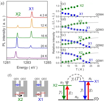
In order to obtain more information about the interdot coupling, we performed temperature-dependent PL measure-ments. Figure 4共a兲 shows such results for QDM1 at T = 4.3– 24 K under a low-excitation power. With the increas-ing temperature, the X1 intensity共I1兲 decreases while the X2
intensity共I2兲 increases with a crossing in relative intensities I1,2/共I1+ I2兲 at T=16 K. As shown in Figs. 4共b兲–4共e兲, the
investigated QDMs exhibited a similar behavior but with dif-ferent crossing temperatures. Because X1 and X2 are direct and indirect transitions 关Fig.4共f兲兴, the intensity crossing in-dicates a directional transfer of hole between the two adja-cent dots. Such directional transfers are thermally activated processes within time scales comparable to the recombina-tion lifetime of the direct exciton X1. To understand the un-derlying transfer processes, a simplified rate-equation model considering an interdot transfer rate ␥t from X1 to X2 was used,10,11
冢
n˙0 n˙1 n˙2冣
=冢
− g1− g2 ␥1 ␥2 g1 −␥1−␥t 0 g2 ␥t −␥2冣冢
n0 n1 n2冣
, 共1兲where n0, n1, and n2are the probability of finding the system
to be in vacuum state, X1 and X2 states; and g1共g2兲 and
␥1共␥2兲 are generation and recombination rates for X1共X2兲, as
schematically shown in Fig. 4共f兲. For simplicity, biexciton states are neglected in this model, which is applicable under low-excitation conditions. To account for the thermal activa-tion behavior, the temperature dependence of interdot trans-fer rate was assumed to be ␥t共T兲=␥0exp共−EA/kBT兲, where the ␥0 is a preexponential factor and EA is the activation energy. Here, the direct coupling between X1 and X2 has been excluded from this simplified model. In fact, if the two hole levels are directly coupled, the population in the ener-getically lower-state X2 would be significantly higher than that in X1 at 4.2 K, since the relaxation bottleneck is not expected for the holes between levels separated by only ⌬E12= 1.3– 2 meV.22–24 For the investigated QDMs, I2ⱗI1
was typically observed at low temperatures共except QDM4兲, indicating that the two hole levels are not directly coupled. On the other hand, because the typical coupling strength of direct hole tunneling is ⱗ1 meV for barrier thickness ⲏ4 nm 共Ref. 25兲, it can be inferred that the hole levels of the two dots are not aligned and hence suppressing the direct hole tunneling.26
By solving the rate equation in steady state, the relative intensity of X1 is given by
-0.2 0.0 0.2 -0.2 0.0 0.2
Relative energy ( meV )
P L in te nsit y ( a. u. ) (a)
XX1
(b) (c) (d)X3
x π 1∆
X1
X2
y π x π y π x π y π x π y πFIG. 3. 共Color online兲 Polarization dependent PL measurements of QDM1. (b) X1 X2 X1 X2 QDM1 (c) QDM2 (d) QDM3 X1 X2 (e) X1 X2 QDM4 1281 1283 1285 24 K 20 K 16 K 12 K PL intensity ( a. u. ) Energy ( eV ) 4.3 K X1 X2 (a) 1, 2 1 2 /( ) II I + 5 10 15 20 25 30 0.0 0.5 1.0 0.0 0.5 1.0 0.0 0.5 1.0 0.0 0.5 1.0 T ( K ) Re la tiv e in ten si ty QD1 QD2 QD1 QD2 1
γ
2γ
g1 2 g ( ) t Tγ
0 n 1 n 2 n X1 |0 X2 X1 X2 (f)FIG. 4. 共Color online兲 共a兲 Temperature-dependent PL spectra of QDM1. 共b兲–共e兲 The relative intensities of X1 and X2 transitions,
I1,2/共I1+ I2兲, as a function of temperature for different QDMs. Solid lines are fitting curves calculated from the rate-equation model.共f兲 Schematics for the direct and indirect transitions as well as the level diagram of the rate-equation model.
I1
I1+ I2
= g1/共g1+ g2兲 1 +共␥0/␥1兲exp共− EA/kBT兲
. 共2兲
The relative intensity of X2 can then be obtained from 1 −关I1/共I1+ I2兲兴. The advantage of analyzing the relative inten-sities I1,2/共I1+ I2兲, instead of absolute intensities I1,2, is that only three fitting parameters are necessary to reproduce the experimental data. The parameters共␥0/␥1兲, EA, and共g1/g2兲
determine the crossing temperature, the slope of intensity variation with temperature, and the intensity ratio I1/I2 at low temperatures,26respectively. As shown in Fig.4, a good agreement is found between the simple model calculation and the experimental data. As for QDM4, the X2 intensity is already stronger than X1 at the lowest temperature; no inten-sity crossing can be observed at elevated temperatures. This indicates that the hole levels in QDM4 are directly coupled at low temperatures, as can be inferred from the very small energy detuning of only⌬E12⬃0.3 meV.
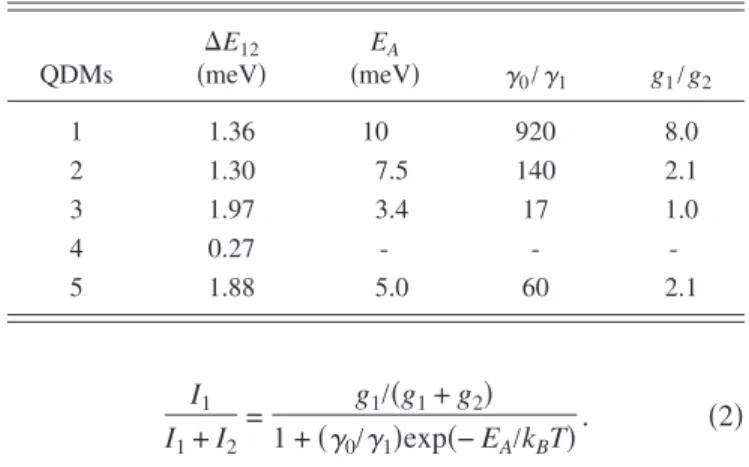
In TableI, the fitting parameters for different QDMs are listed, together with their energy separation ⌬E12 between X1 and X2. The fitted values of EA,共␥0/␥1兲, and 共g1/g2兲 did
not show noticeable correlation with ⌬E12. However, we
found that the ␥0/␥1 shows an exponential dependence on
EA. This can be explained by a thermally activated tunneling of the hole from one dot to another, as schematically illus-trated in Fig.5共a兲. The hole in QD1 first absorbed the ther-mal energy共EA兲 and is activated to a higher-lying hole level, and then it is tunneled into QD2 followed by rapid relax-ations to form an indirect exciton X2. For a square tunneling barrier, the interdot tunneling rate can be approximated by
␥tun⬀exp关−2d
冑
共2mhⴱ⌬V/ប2兲兴, which increases exponentially with the reducing barrier height ⌬V and thickness d. This explains why the interdot hole transfer can be considerably enhanced by the absorption of thermal energy 共acoustic phonons兲 to available higher-lying levels, because from which the tunneling barrier height is effectively reduced. Quantitatively, the total transfer rate␥tvia such a thermally activated tunneling is determined by the product of␥tunand the thermionic emission rate. Therefore, the preexponential factor␥0in Eq.共2兲 would involve␥tun, i.e.,␥0⬀␥tun. Figure 5共b兲 shows a semilogarithmic plot of the fitted ␥0/␥1 for different QDMs to the estimated冑
⌬V, where ⌬V=共Vh− EA兲 and Vh= 20 meV were used.27 Such an exponential depen-dence clearly demonstrates that the directional energy trans-fer is a thermally activated tunneling, rather than direct tun-neling or dipole-dipole Förster transfers.For QDMs formed by two nonidentical dots with notice-ably different sizes, the direct excitons in different dots would have a large energy difference, which can substan-tially suppress the dipole-dipole interactions. Even though a phonon-assisted Förster transfer was taken into account,10,11 i.e., the two direct excitons in different dots were brought into resonance via absorption of thermal energy, the deduced
␥0 should be independent of EA and should reflect the strength of dipole-dipole interaction, which depends only on the interdot separation and cannot account for the observed exponential dependence of␥0on
冑
⌬V.Our results have an important implication for the control of interdot coupling in a QDM. Electric-field tuning of inter-dot tunnel coupling was the most successful. However, our results indicated that the thermally activated tunneling of the hole opens another channel for interdot coupling at elevated temperatures, even though the two ground hole levels are detuned from resonance. This would make the electric-field tuning of interdot coupling between hole levels become less controllable, particularly at higher temperatures. Such a ther-mally activated tunneling would be less significant between electron levels because the confined potential and the inter-level spacing of electron inter-levels are usually significantly larger than that of hole levels.
In summary, we presented a spectroscopic study of single QDMs formed by two closely stacked In0.5Ga0.5As QD
lay-ers. The exciton fine structures, as well as direct and indirect excitonic species associated with QDMs, were identified by power dependent and polarization resolved microphotolumi-nescence measurements. As the temperature was increased, a directional energy transfer between the direct and indirect excitons in single QDMs was observed. A rate-equation model was developed to explain our data. We showed that the origin of the directional energy transfers in QDMs is a thermally activated tunneling of the hole between the two adjacent dots, rather than a direct tunneling or dipole-dipole Förster transfers. Such a nonresonant carrier transfer should be considered in the control of hole level coupling in QDMs at higher temperatures.
This work was supported in part by the program of MOE-ATU and the National Science Council of Taiwan under Grant No. NSC-96–2112-M-009–014.
TABLE I. Fitting parameters EA,共␥0/␥1兲, and 共g1/g2兲 for
dif-ferent QDMs. The energy separation⌬E12between X1 and X2 are also listed for comparison.
QDMs ⌬E12 共meV兲 EA 共meV兲 ␥0/␥1 g1/g2 1 1.36 10 920 8.0 2 1.30 7.5 140 2.1 3 1.97 3.4 17 1.0 4 0.27 - - -5 1.88 5.0 60 2.1 A
E
γ
tun QD1 QD2 (a) (b) hV
d
V ∆ 1/ 2 1/2 (Vh−EA) (meV) 01 (/ )γ
γ
2.8 3.2 3.6 4.0 4.4 101 102 103FIG. 5.共Color online兲 共a兲 Schematic processes for the thermally activated tunneling of hole between the two adjacent QDs.共b兲 A semilog plot of the fitted value of ␥0/␥1 for different QDMs as
function of共Vh− EA兲1/2, where V
1P. Michler, A. Kiraz, C. Becher, W. V. Schoenfeld, P. M. Petroff,
L. Zhang, E. Hu, and A. Imamoglu, Science 290, 2282共2000兲; M. Pelton, C. Santori, J. Vučković, B. Zhang, G. S. Solomon, J. Plant, and Y. Yamamoto, Phys. Rev. Lett. 89, 233602共2002兲; Z. Yuan, B. E. Kardynal, R. M. Stevenson, A. J. Shields, C. J. Lobo, K. Cooper, N. S. Beattie, D. A. Ritchie, and M. Pepper, Science 295, 102 共2002兲; W.-H. Chang, W.-Y. Chen, H.-S. Chang, T.-P. Hsieh, J.-I. Chyi, and T.-M. Hsu, Phys. Rev. Lett.
96, 117401共2006兲.
2X. Li, Y. Wu, D. Steel, D. Gammon, T. H. Stievater, D. S.
Katzer, D. Park, C. Piermarocchi, and L. J. Sham, Science 301, 809共2003兲.
3H. J. Krenner, M. Sabathil, E. C. Clark, A. Kress, D. Schuh, M.
Bichler, G. Abstreiter, and J. J. Finley, Phys. Rev. Lett. 94, 057402共2005兲.
4G. Ortner, M. Bayer, Y. Lyanda-Geller, T. L. Reinecke, A. Kress,
J. P. Reithmaier, and A. Forchel, Phys. Rev. Lett. 94, 157401 共2005兲.
5H. J. Krenner, E. C. Clark, T. Nakaoka, M. Bichler, C. Scheurer,
G. Abstreiter, and J. J. Finley, Phys. Rev. Lett. 97, 076403 共2006兲.
6E. A. Stinaff, M. Scheibner, A. S. Bracker, I. V. Ponomarev, V.
L. Korenev, M. E. Ware, M. F. Doty, T. L. Reinecke, and D. Gammon, Science 311, 636共2006兲; M. F. Doty, M. Scheibner, I. V. Ponomarev, E. A. Stinaff, A. S. Bracker, V. L. Korenev, T. L. Reinecke, and D. Gammon, Phys. Rev. Lett. 97, 197202共2006兲.
7M. Scheibner, M. F. Doty, I. V. Ponomarev, A. S. Bracker, E. A.
Stinaff, V. L. Korenev, T. L. Reinecke, and D. Gammon, Phys. Rev. B 75, 245318共2007兲.
8M. Scheibner, I. V. Ponomarev, E. A. Stinaff, M. F. Doty, A. S.
Bracker, C. S. Hellberg, T. L. Reinecke, and D. Gammon, Phys. Rev. Lett. 99, 197402共2007兲.
9G. J. Beirne, C. Hermannstädter, L. Wang, A. Rastelli, O. G.
Schmidt, and P. Michler, Phys. Rev. Lett. 96, 137401共2006兲.
10A. O. Govorov, Phys. Rev. B 71, 155323共2005兲.
11B. D. Gerardot, S. Strauf, M. J. A. de Dood, A. M. Bychkov, A.
Badolato, K. Hennessy, E. L. Hu, D. Bouwmeester, and P. M. Petroff, Phys. Rev. Lett. 95, 137403共2005兲.
12S. Yamauchi, K. Komori, I. Morohashi, K. Goshima, T. Sugaya,
and T. Takagahara, Appl. Phys. Lett. 87, 182103共2005兲.
13H. Gotoh, H. Sanada, H. Kamada, H. Nakano, S. Hughes, H.
Ando, and J. Temmyo, Phys. Rev. B 74, 115322共2006兲.
14A. Tackeuchi, T. Kuroda, K. Mase, Y. Nakata, and N. Yokoyama,
Phys. Rev. B 62, 1568共2000兲.
15Yu. I. Mazur, Zh. M. Wang, G. G. Tarasov, Min Xiao, G. J.
Salamo, J. W. Tomm, V. Talalaev, and H. Kissel, Appl. Phys. Lett. 86, 063102共2005兲.
16M. Reischle, G. J. Beirne, R. Roßbach, M. Jetter, H. Schweizer,
and P. Michler, Phys. Rev. B 76, 085338共2007兲.
17T.-P. Hsieh, H.-S. Chang, W.-Y. Chen, W.-H. Chang, T. M. Hsu,
N.-T. Yeh, W.-J. Ho, P.-C. Chiu, and J.-I. Chyi, Nanotechnology
17, 512共2006兲.
18W.-H. Chang, H.-S. Chang, W.-Y. Chen, T. M. Hsu, T.-P. Hsieh,
J.-I. Chyi, and N.-T. Yeh, Phys. Rev. B 72, 233302共2005兲.
19G. Bester, J. Shumway, and A. Zunger, Phys. Rev. Lett. 93,
047401共2004兲.
20M. Bayer, G. Ortner, O. Stern, A. Kuther, A. A. Gorbunov, A.
Forchel, P. Hawrylak, S. Fafard, K. Hinzer, T. L. Reinecke, S. N. Walck, J. P. Reithmaier, F. Klopf, and F. Schäfer, Phys. Rev. B
65, 195315共2002兲.
21A. Högele, S. Seidl, M. Kroner, K. Karrai, R. J. Warburton, B. D.
Gerardot, and P. M. Petroff, Phys. Rev. Lett. 93, 217401共2004兲.
22R. Heitz, A. Kalburge, Q. Xie, M. Grundmann, P. Chen, A.
Hoff-mann, A. Madhukar, and D. Bimberg, Phys. Rev. B 57, 9050 共1998兲.
23G. Ortner, R. Oulton, H. Kurtze, M. Schwab, D. R. Yakovlev, M.
Bayer, S. Fafard, Z. Wasilewski, and P. Hawrylak, Phys. Rev. B
72, 165353共2005兲.
24T. Nakaoka, E. C. Clark, H. J. Krenner, M. Sabathil, M. Bichler,
Y. Arakawa, G. Abstreiter, and J. J. Finley, Phys. Rev. B 74, 121305共R兲 共2006兲.
25A. S. Bracker, M. Scheibner, M. F. Doty, E. A. Stinaff, I. V.
Ponomarev, J. C. Kim, L. J. Whitman, T. L. Reinecke, and D. Gammon, Appl. Phys. Lett. 89, 233110共2006兲.
26If the two hole levels are not too far away from resonance, a
slow direct tunneling rate may contribute to the interdot transfer rate, which will alter the intensity ratio I1/I2at low
tempera-tures. Within our model fitting, this effect has been incorporated into the ratio of generation rates g1/g2so that the direct tunnel-ing component was not included in␥t共T兲.
27The energy difference between the QDM emissions and the WL
peak is⬃70 meV. Adopting a ratio of Ve: Vh= 7 : 3 between the
electron and hole confined potentials, the hole confined potential is estimated to be Vh⬃20 meV.