IEEE PHOTONICS TECHNOLOGY LETTERS, VOL. 25, NO. 1, JANUARY 1, 2013 97
Improved 1.3-
µm Electroluminescence of
InGaAs-Capped Type-II GaSb/GaAs Quantum
Rings at Room Temperature
Wei-Hsun Lin, Student Member, IEEE, Kai-Wei Wang, Shih-Yen Lin, Senior Member, IEEE,
and Meng-Chyi Wu, Senior Member, IEEE
Abstract— Room-temperature 1.3-µm electroluminescence is observed for the InGaAs-capped GaSb quantum rings (QRs). The increasing carrier density in the InGaAs-capped type-II GaSb QRs would induce a larger blue shift in the same laser pumping power span and enhance the luminescence intensity. The enhanced luminescence intensity, a larger blue shift of peak wavelength, and 1.3-µm emission of the InGaAs-capped QR structure have revealed its potential application in multi-wavelength light-emitting devices in the near infrared range.
Index Terms— GaSb quantum rings, light-emitting devices.
I. INTRODUCTION
O
NE of the major differences between photo-luminescence (PL) of type-I and type-II hetero-structures is the blue peak shift of the type-II heterostructure with increasing laser pumping power [1]–[3]. Although this unique characteristic can be useful for multi-wavelength emission of light-emitting devices, reports regarding to such applications are very limited since weak luminescence at low temperatures is usually observed for type-II heterostructures [4], [5]. In one of our previous publications, room-temperature electroluminescence (EL) of type-II GaSb/GaAs quantum dots (QDs) is observed [6]. With precisely controlling Sb flux/background As ratios during the post-growth soaking procedure, the GaSb QDs can be fully converted into quantum rings (QRs). The more intense photoluminescence (PL) intensity of QRs compared with QDs is attributed to the less abrupt GaSb/GaAs interfaces and more surrounding electron shells over the GaSb QRs [7]. Compatible luminescence intensity compared to the traditional InAs QDs is alsoManuscript received August 6, 2012; revised September 19, 2012; accepted November 15, 2012. Date of publication November 29, 2012; date of current version December 20, 2012. This work was supported in part by the National Science Council, Taiwan under Grant NSC 101-2628-E-001 -001 and in part by Nano-Project Granted by Academia Sinica.
W.-H. Lin, and M.-C. Wu are with the Institute of Electronics Engi-neering, National Tsing Hua University, Hsinchu 300, Taiwan (e-mail: [email protected]; [email protected]).
K.-W. Wang is with the College of Photonics, National Chiao-Tung University, Tainan 711, Taiwan (e-mail: [email protected]).
S.-Y. Lin is with the Research Center for Applied Sciences, Academia Sinica, Taipei 11529, Taiwan, and also with the Department of Photonics, National Chiao-Tung University, Hsinchu 300, Taiwan, and also with the Institute of Optoelectronic Sciences, National Taiwan Ocean University, Keelung 20224, Taiwan (e-mail: [email protected]).
Color versions of one or more of the figures in this letter are available online at http://ieeexplore.ieee.org.
Digital Object Identifier 10.1109/LPT.2012.2229700
observed for the type-II coupled GaSb QR structure [8]. These works have revealed the potential of the type-II GaSb QRs for light-emitting diode (LED) applications. The pursuit of 1300-nm diode lasers on GaAs substrate had been motivated by the need to achieve high performance uncooled lasers operating up to high temperature [9], [10]. Recent works by using InGaAsN or InGaAs quantum wells (QWs) had led to very low threshold and high power diode lasers emitting in the range of 1300-nm spectral regime [9], [10]. W-shape type-II QWs have also demonstrated long wavelength emission ranging 1400–1600 nm [11]. Therefore, if luminescence enhancement can be achieved in the communication-wavelength range, the type-II GaSb QRs can be very useful for multi-wavelength LEDs in the near infrared range.
In this letter, room-temperature 1.3 µm EL is observed for the InGaAs-capped GaSb QRs. Compared with standard QRs, around two-order-of-magnitude PL intensity enhance-ment is observed for this structure. The improveenhance-ment of PL intensity enhancement is attributed to the enhanced electron confinement and larger electron-hole wave function overlap of the structure. The increasing carrier density in the InGaAs-capped type-II GaSb QRs has also induced a larger blue shift in the same laser pumping power span. Therefore, with the insertion of InGaAs capped layers, not only the luminescence is enhanced, the tuning range of the type-II GaSb QR LED is also enlarged, which are advantageous for the application of multi-wavelength LEDs.
II. EXPERIMENTS
The samples investigated in this study were grown on (100)-oriented semi-insulated GaAs substrates by using a Riber C21 solid-source molecular beam epitaxy system. Two samples with three-period GaSb/GaAs QRs with and without 10 nm In0.15Ga0.85As capped layers were prepared, which
are referred as samples A and B, respectively. To obtain the morphology of the GaSb QRs, additional uncapped GaSb QR layers were grown on the two samples for atomic force microscopy (AFM) measurements. The sample structures are shown in Table I. The detail growth procedure for the QR structures is reported elsewhere [7]. For EL measure-ments, an additional sample of a GaAs PIN diode structure with the same active region as sample B was prepared. Three-period 10 nm In0.15Ga0.85As capped GaSb QRs are 1041–1135/$31.00 © 2012 IEEE
98 IEEE PHOTONICS TECHNOLOGY LETTERS, VOL. 25, NO. 1, JANUARY 1, 2013
TABLE I
WAFERSTRUCTURES OFSAMPLESAANDB
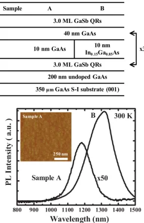
350 μm GaAs S-I substrate (001) 200 nm undoped GaAs Sample 10 nm In0.15Ga0.85As x3 A 3.0 ML GaSb QRs 10 nm GaAs 40 nm GaAs 3.0 ML GaSb QRs B 800 900 1000 1100 1200 1300 1400 1500 300 K x50 B Sample A P L I n te n sit y ( a. u . ) Wavelength (nm) 250 nm Sample A
Fig. 1. Room-temperature PL spectra of samples A and B with laser pumping power density of 0.5 W/cm2. Insert: 1× 1 m2AFM image of sample A.
inserted in a 200 nm undoped GaAs layer and sandwiched between 300 nm GaAs bottom contact layer n-type doped to 2 × 1018 cm−3 and 300 nm GaAs top contact layer p-type doped to 2 × 1018 cm−3. With the grid top contact metal, a
630× 450 µm2light-emitting device was fabricated.
III. RESULTS ANDDISCUSSION
The 1 × 1 µm2 AFM image of sample A is shown in the insert of Fig. 1. As shown in this figure, whole ring morpholo-gies are observed for sample A. Similar QR morpholomorpholo-gies are also observed for sample B. The room-temperature PL spectra of samples A and B measured at the pumping power density of 0.5 W/cm2 are shown in Fig. 1. An inspection of this figure reveals that the PL wavelength shifts to 1.3 µm for sample B, which is attributed to the lowering conduction band edge of the InGaAs capped layer. Also observed in this figure is the around two-order-of magnitude luminescence enhancement of sample B as compared to that of sample A. Since for the type-II heterostructure, electrons and holes are confined separately on either side of the interface, the low optical recombination probability of electron-hole pairs is the nature of such a structure. In this case, it is less possible that the significant luminescence enhancement of sample B is resulted from the enhanced recombination rate. The possible mechanism responsible for this phenomenon should be the better carrier confinement of sample B.
GaAs Barrier GaSb QR GaAs Barrier GaAs Barrier GaSb QR GaAs Barrier InGaAs Layer
Sample A Sample B Electron
Hole Light Irradiation
Light Irradiation
Fig. 2. Schematic band diagrams of samples A and B.
To further investigate this phenomenon, the schematic band diagrams of the two samples are shown in Fig. 2. Since the large valence-band offset is observed for GaSb/GaAs interfaces [8], the hole storage time in the GaSb QRs should be similar for the two samples. In this case, the major difference between the two samples should be the lifetime of electrons staying near the GaSb/(InGa)As interfaces. For sample A, although the holes in the GaSb QRs will induce more electron accumulation in the GaAs region than those in the GaSb QDs, the electrons still have higher possibility of escaping to the bulk GaAs region away from the interface. Therefore, the reduced electron number near the hetero-interfaces will result in a weaker PL intensity. For sample B, with the additional InGaAs capped layer, the GaAs/InGaAs interface will provide an additional barrier to prevent the electrons escaping from the InGaAs/GaSb interface. The increasing electron number in the InGaAs-capped QR structure will therefore result in the two-order-of-magnitude PL intensity enhancement of sample B than that in sample A.
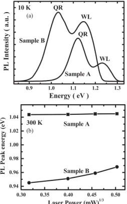
The supporting evidence of electrons escaped away from the GaAs/GaSb interface for sample A at room temperature may come from its low-temperature PL spectrum. The 10 K PL spectra of samples A and B are shown in Fig. 3(a). Not like the two-order-of-magnitude PL intensity enhancement, the PL intensity of sample B is only about one time higher than that of sample A. The results suggest that at low temperatures, the probability of electrons escaping away from GaAs/GaSb interfaces is reduced. In this case, the PL intensity of sample A would be greatly enhanced. Also shown in this figure is the appearance of wetting-layer (WL) luminescence [4]. The red shift of WL peak of sample B is attributed to the conduction band edge lowering of the InGaAs capped layers. The other supporting evidence comes from the PL results of laser pumping power dependence for the two samples. The room-temperature PL peak energy of the two samples observed under different laser pumping power densities are shown in Fig. 3(b). It is observed that the blue shift of PL peak has a linear dependence over the cubic root of laser pumping power densities. This confirms that the observed luminescence is from type-II heterostructures. Also shown in this figure is the larger energy of blue shift in the same laser pumping power density span for sample B. It has been previously predicted that a higher carrier concentration would lead to a larger
LIN et al.: IMPROVED 1.3-µm EL OF InGaAs-CAPPED TYPE-II GaSb/GaAs QR AT ROOM TEMPERATURE 99 0.9 1.0 1.1 1.2 1.3 QR QR WL WL Sample A Sample B 10 K PL Intensity ( a.u. ) Energy ( eV ) 0.30 0.35 0.40 0.45 0.50 0.94 0.96 0.98 1.00 1.02 1.04 Sample B Sample A 300 K
PL Peak energy (eV
)
Laser Power (mW)1/3
(a)
(b)
Fig. 3. (a) 10 K PL spectral measured at the laser pumping power density of 0.5 W/cm2. (b) Room-temperature PL peak energy observed under different laser pumping power densities for samples A and B.
900 1000 1100 1200 1300 1400 1500 Top contant Botton contant Meas and window 300 K 0.72 V 0.86 V 0.94 V Normalized EL Intensity ( a.u. ) Wavelength (nm)
Fig. 4. Room-temperature EL spectra of the device with the same active region of sample B at 25-Hz pulsed voltages of 0.94, 0.86, and 0.72 V. Insert: Top-view picture of the device.
blue shift of PL peak for type-II heterostructures [12]. The larger blue shift of PL peak for sample B has confirmed the attribution that higher carrier concentrations are in the type-II heterostructures. The same phenomenon would also induce the enhanced PL intensity of sample B.
The room-temperature EL spectra of the GaAs PIN diode with the same active region as sample B at 25-Hz pulsed voltages of 0.94, 0.84 and 0.72 V are shown in the Fig. 4. The corresponding injection current densities are 0.147, 0.0834 and 0.0298 A/cm2, respectively. The EL peak wavelength shifts from 1332 to 1252 nm with increasing injection current
densities. It demonstrates that the room-temperature 1.3 µm EL can be easily achieved by using the type-II InGaAs-capped GaSb QR structure. The large wavelength tuning over 80 nm has also demonstrated the potential of such structures in the application of multi-wavelength LED in the near infrared range. Additional carrier confinement layers such as AlGaAs layers sandwiching the active region may further enhance the wavelength-tuning range and EL intensity of the InGaAs-capped type-II GaSb QR structures.
IV. CONCLUSION
In conclusion, the intense room-temperature 1.3 µm EL is observed for the InGaAs-capped GaSb QR structuers. Com-pared with standard QRs, around two-order-of-magnitude PL intensity enhancement is observed for the structure. With the insertion of InGaAs capped layers, not only the emitting wave-length is extended to 1.3µm, enhanced luminescence intensity and a larger blue shift of luminescence peak are also observed for the device. The results have demonstrated the potential application of such structures in multi-wavelength LEDs in the near infrared range. To further enhance the luminescence intensity and the wavelength tuning range, the addition of other carrier confinement layers may achieve the goals in the future.
REFERENCES
[1] F. Hatami, et al., “Radiative recombination in type-II GaSb/GaAs quantum dots,” Appl. Phys. Lett., vol. 67, no. 5, pp. 656–658, 1995. [2] J. Tatebayashi, et al., “Time-resolved photoluminescence of type-II
Ga(As)Sb/GaAs quantum dots embedded in an InGaAs quantum well,”
Nanotechnology, vol. 19, pp. 295704–295709, May 2008.
[3] C. C. Tseng, et al., “The influence of As on the morphologies and optical characteristics of GaSb/GaAs quantum dots,” IEEE J. Quantum
Electron., vol. 47, no. 3, pp. 335–339, Mar. 2011.
[4] C. K. Sun, et al., “Optical investigations of the dynamic behavior of GaSb/GaAs quantum dots,” Appl. Phys. Lett., vol. 68, no. 3, pp. 1543–1545, 1996.
[5] R. J. Young, E. P. Smakman, A. M. Sanchez, P. Hodgson, P. M. Koen-raad, and M. Hayne, “Optical observation of single-carrier charging in type-II quantum ring ensembles,” Appl. Phys. Lett., vol. 100, no. 8, pp. 082101–082104, 2012.
[6] S. Y. Lin, et al., “Room-temperature operation type-II GaSb/GaAs quantum-dot infrared light-emitting diode,” Appl. Phys. Lett., vol. 96, no. 12, pp. 123501–123503, 2010.
[7] W. H. Lin, M. Y. Lin, S. Y. Wu, and S. Y. Lin, “Room-temperature electro-luminescence of type-II GaSb/GaAs quantum rings,” IEEE
Pho-ton. Technol. Lett., vol. 24, no. 14, pp. 1203–1205, Jul. 15, 2012.
[8] W. H. Lin, K. W. Wang, S. W. Chang, M. H. Shih, and S. Y. Lin, “Type-II GaSb/GaAs coupled quantum rings: Room-temperature lumi-nescence enhancement and recombination lifetime elongation for device applications,” Appl. Phys. Lett., vol. 101, no. 3, pp. 031906-1–031906-4, 2012.
[9] N. Tansu, J. Y. Yeh, and L. J. Mawst, “Physics and characteristics of 1200-nm InGaAs and 1300–1400 nm InGaAsN quantum-well lasers by metalorganic chemical vapor deposition,” J. Phys., Conden. Matter
Phys., vol. 16, no. 31, pp. 3277–3318, 2004.
[10] N. Tansu, “Current injection efficiency of InGaAsN quantum-well lasers,” J. Appl. Phys., vol. 97, no. 5, pp. 054502–054518, 2005. [11] J. Y. Yeh, et al., “Long wavelength emission of InGaAsN/GaAsSb
type-II W quantum wells,” Appl. Phys. Lett., vol. 88, no. 5, pp. 051115–051118, 2006.
[12] D. Alonso-Álvarez, B. Alén, J. M. García, and J. M. Ripalda, “Optical investigation of type II GaSb/GaAs self-assembled quantum dots,” Appl.