Nitrogen-induced enhancement of the electron effective mass
in InN
xAs
1ÀxW. K. Hung, K. S. Cho, M. Y. Chern, and Y. F. Chena)
Department of Physics, National Taiwan University, Taipei, Taiwan, Republic of China D. K. Shih and H. H. Lin
Department of Electrical Engineering, National Taiwan University, Taipei, Taiwan, Republic of China C. C. Lu and T. R. Yang
Department of Physics, National Taiwan Normal University, Taipei, Taiwan, Republic of China 共Received 6 September 2001; accepted for publication 14 November 2001兲
The electron effective mass in n-type InNxAs1⫺x 共with x up to 3.0%兲 grown by gas-source
molecular-beam epitaxy was obtained from infrared reflectivity and Hall-effect measurements. The large increase of the effective mass due to the incorporation of nitrogen is attributed mainly to the nitrogen-induced modification on the electronic states near the conduction-band edge. The well-known band anticrossing共BAC兲 model for the electronic structure of the III-N-V alloys cannot well describe the experimental data, especially in the region of higher electron concentration. This result provides an opportunity to examine the ‘‘universality’’ of the BAC model. © 2002 American Institute of Physics. 关DOI: 10.1063/1.1436524兴
III-N-V alloys such as Ga共In兲NAs, GaNP, and InNP have been found to exhibit particular physical properties and po-tential applications in long-wavelength optoelectronic devices.1– 6The incorporation of nitrogen into the host III–V crystal causes a significant reduction 共giant bowing兲 in the fundamental band gap,4,5 reduced temperature and pressure dependence of the band-gap energy,7,8and a large increase in the electron effective mass.9–11These unusual behaviors are usually explained in terms of the band anticrossing 共BAC兲 model in which the localized N resonant states interact with the extended conduction-band 共CB兲 states, leading to the splitting of the CB into two nonparabolic subbands.7 Alter-natively, the theoretical calculations based on the pseudopo-tential local density approximation indicates that the N-induced mixing between the ⌫ and L states is responsible for these phenomena.12
InNxAs1⫺x should be a promising material for infrared
technology since InAs has a narrow band gap of 0.36 eV at room temperature. Up to now, there were only very limited efforts directed to this alloy.13–15Naoi, Naoi, and Sakai grew InNAs films on GaAs substrates by metalorganic chemical-vapor deposition and found the band gap reduced to 0.12 eV with nitrogen composition up to 6%.13However, except for a photoluminescence study on InNxAs1⫺x/InGaxAs1⫺x single
quantum wells,15no further experimental studies on the elec-tronic properties of InNAs were reported. Knowledge of the carrier effective mass provides valuable information on the fundamental nature of the band states in the alloy and is also important for a full exploration and optimization of this ma-terial system in device applications. In this work, we report measurements of the electron effective mass in InNxAs1⫺x with various N contents and electron concentrations. The ef-fective mass is greatly enhanced due to the N incorporation. However, in contrast to the case of Ga共In兲NAs, we find that
the simple BAC model may be not suitable to describe the effective mass in the InNAs alloy systems.
The InNAs films were grown on semi-insulating 共001兲 InP substrates using a VG V-80 gas-source molecular-beam epitaxy system. An element In source and thermally cracked AsH3 were used for producing molecular beams. The active
N species were generated from an EPI UNI-bulb rf plasma source. The growth temperature for InNAs was 460 °C. De-tails of the growth conditions are reported elsewhere.16The films are about 2.5m thick and intentionally undoped. The samples were examined with a high-resolution x-ray diffrac-tometer using the Cu K␣1 line 共with wavelength 1.54 Å兲.
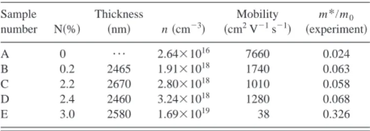
The N compositions were determined by assuming that the InNAs films are fully relaxed and Vegard’s law holds. The former assumption is justified by the fact that the film thick-ness is much larger than the critical thickthick-ness calculated from the Matthews and Blakeslee model.17 The lattice con-stants of InP, InAs, and cubic InN are taken to be 5.8688, 6.0584, and 4.98 Å, respectively. The electrical properties were investigated by Hall-effect measurements in the Van der Pauw configuration. The results are summarized in Table I. The samples containing nitrogen are intrinsically n type and the electron concentration increases with the incorpo-rated N concentration. The possible origin of the high carrier concentration in these samples is not yet clear.
The infrared reflectivity measurements were performed
a兲Electronic mail: yfchen@phys.ntu.edu.tw
TABLE I. Parameters of the studied samples. All measurements were per-formed at room temperature.
Sample number N共%兲 Thickness 共nm兲 n共cm⫺3兲 Mobility 共cm2V⫺1s⫺1兲 m */m0 共experiment兲 A 0 ¯ 2.64⫻1016 7660 0.024 B 0.2 2465 1.91⫻1018 1740 0.063 C 2.2 2670 2.80⫻1018 1010 0.058 D 2.4 2460 3.24⫻1018 1280 0.068 E 3.0 2580 1.69⫻1019 38 0.326
APPLIED PHYSICS LETTERS VOLUME 80, NUMBER 5 4 FEBRUARY 2002
796
at room temperature with a Bruker IFS 120 HR Fourier transform infrared spectrometer. Figure 1共a兲 shows the re-flectivity spectra of three InNxAs1⫺xsamples. The features at about 307.2 and 347.5 cm⫺1 correspond to InP transverse optical共TO兲 and longitudinal optical 共LO兲 phonons, respec-tively. We attribute the peak at about 225 cm⫺1to the InAs-like TO mode, and the peak at about 440 cm⫺1 to the InN-like TO mode. The plasma reflection edge is evidently observed and shifts to higher energy with increasing electron concentration.
Electron effective mass m* is obtained by fitting the reflectivity spectra with a three-layer structure共air–InNAs– InP兲 model. The dielectric function of InP is taken from the literature. Dielectric function ⑀ of InNAs can be modeled with an additive form18
⑀⫽⑀⬁⫹
兺
j⫽1 2 Sj T j 2 ⫺ 2⫺i⌫ j ⫺ ⑀⬁p 2 共⫹i␥兲, 共1兲where⑀⬁ is the high-frequency dielectric constant共taken to be 12.25, the same as InAs兲; T j, ⌫j, and Sj are the reso-nance frequency, damping constant, and strength of the jth TO mode共InAs and InN-like兲, respectively. The last term in Eq. 共1兲 represents the free-carrier contribution with
frequency-independent damping constant ␥ and plasma fre-quencyp. The electron effective mass at the Fermi energy
can be determined from18,19
m*⫽4ne
2
⑀⬁p
2 , 共2兲
where e is the electron charge, and n is the electron concen-tration. The obtained values of the film thickness and effec-tive mass are also listed in Table I. We see that the effeceffec-tive mass increases largely as nitrogen atoms are introduced into the InAs host.
The experimental effective mass obtained above is plot-ted against the electron concentration in Fig. 2. It is well known that due to the CB nonparabolicity the electron effec-tive mass in heavily doped narrow-band-gap semiconductors strongly depends on the electron concentration. To evaluate this effect, we use the simple two-band Kane model20,21to calculate the InAs effective mass mMat the electron
concen-tration of our samples. The momentum matrix element P2in the Kane model is taken to be 11.9 eV, as in Ref. 20, and the results are consistent with the values found in the literature.20 The calculated mM, also plotted in Fig. 2, is too small to
account for the experimental data. Thus, it is clear that the enhancement of the effective mass should be mainly due to the N-induced modification of the CB structure.
The BAC model is known to predict a large increase of the electron effective mass.10,22In the model, the interaction of N states with the extended states of the semiconductor matrix results in the formation of two conduction subbands E⫺and E⫹ given by7
E⫾共k兲⫽1
2兵关EM共k兲⫹EN兴⫾
冑
关EM共k兲⫺EN兴 2⫹4CN M
2 x其,
共3兲 where EN is the energy of the N state, EM(k) is the disper-sion relation for the CB of the host crystal, and CN M is the matrix element describing the coupling between these two types of states. All the energies are relative to the top of the valence band. Due to its localized nature, the energy ENof
the N level can be estimated to be 1.48 eV from valence-band offset ⌬ (GaAs/InAs)⫽0.17 eV and from EN FIG. 1. 共a兲 Reflectivity spectra for three InNxAs1⫺xsamples.
FIG. 2. Effective mass vs electron concentra-tion n. Closed circles denote the experimental data for InNxAs1⫺x, while open circles denote
the calculated effective mass for InAs.
797 Appl. Phys. Lett., Vol. 80, No. 5, 4 February 2002 Hunget al.
⫽1.65 eV in GaAs.7,23 C
N M is taken as 1.92 eV to fit the
band-gap energy measured by Naoi, Naoi, and Sakai.13 It should be noted that in the simple BAC model only the an-ticrossing interaction between the extended states of the ⌫ CB and the localized N level is considered. The interaction between L 共or X兲 and the N level is neglected due to the symmetry selection rules.24
From Eq.共3兲 an analytic expression for the k dependence of the inverse effective mass can be written as 共considering only the E⫺branch兲10
1 m*共k兲⫽ 1 2mM共k兲
再
1⫺ 关EM共k兲⫺EN兴冑
关EM共k兲⫺EN兴2⫹4CN M 2 x冎
, 共4兲 where energy-dependent mM(k) and EM(k) are calculated bythe two-band Kane model, as mentioned above. The effective mass is calculated at the Fermi surface, i.e., at k⫽kF
⫽(32n)1/3. One notes that due to the relatively large
en-ergy difference between EN and EM 关EN⫺EM(kF)⬃1 eV,
here兴, the composition-dependent term CN M2 x has little effect on the effective mass. That is, m* should approximately ap-proach mM for InAs. Furthermore, one should note that
ef-fective mass m*(k) calculated from Eq.共4兲 never exceeds 2mM(k) if EM(k)⬍EN. However, as shown in Fig. 2, the
measured effective mass either approaches 2mM, which
cor-responds to extremely large CN M, or exceeds 2 mM
共espe-cially for the sample with the highest electron concentration兲. Thus, the simple BAC model fails to describe the experimen-tal data.
According to our experimental results, it seems more plausible to view the CB edge of InNxAs1⫺x as a mixing
state which has components of the⌫, L, and X states of InAs. Such a mixing is caused by the strong perturbation intro-duced by substitution of N on an As site.12As illustrated in the case of GaNxAs1⫺x, the CB edge shows a reduced 共in-creased兲 ⌫(L) character as x increases 共for x approaches 0.8%, the L component approaches 12%兲.12Since the L elec-trons have much heavier mass than the ⌫ 关for InAs, mt(L)
⬃0.05, ml(L)⬃0.64兴, effective mass m*(kF) has the
possi-bility to exceed 2mM.
In summary, the effective mass of InNxAs1⫺x with
dif-ferent N compositions and electron concentrations was ob-tained from infrared reflectivity and Hall-effect measure-ments. We point out that the large increase of the effective mass is probably due to the N-induced modification on the
electronic structure near the conduction-band edge. Our re-sults, therefore, calls for further theoretical efforts in order to clarify the role of the nitrogen state in the perturbation of the band structure.
This work was supported by the National Science Coun-cil and Ministry of Education of the Republic of China.
1I. A. Buyanova, W. M. Chen, and B. Monemar, MRS Internet J. Nitride
Semicond. Res. 6, 1共2001兲.
2M. Kondow, K. Uomi, T. Kitatani, S. Watahiki, and Y. Yazawa, J. Cryst.
Growth 164, 175共1996兲.
3
G. S. Kinsey, D. W. Gotthold, A. L. Holmes, Jr., B. G. Streetman, and J. C. Campbell, Appl. Phys. Lett. 76, 2824共2000兲.
4J. F. Geisz, D. J. Friedman, J. M. Olson, S. R. Kurtz, and B. M. Keyes, J.
Cryst. Growth 195, 401共1998兲.
5
M. Weyers, M. Sato, and H. Ando, Jpn. J. Appl. Phys., Part 2 31, L853 共1992兲.
6K. M. Yu, W. Walukiewicz, J. Wu, J. W. Beeman, J. W. Ager III, E. E.
Haller, W. Shan, H. P. Xin, and C. W. Tu, Appl. Phys. Lett. 78, 1077 共2001兲.
7
W. Shan, W. Walukiewicz, J. W. Ager III, E. E. Haller, J. F. Geisz, D. J. Friedman, J. M. Olson, and S. R. Kurtz, Phys. Rev. Lett. 82, 1221共1999兲.
8I. Suemune, K. Uesugi, and W. Walukiewicz, Appl. Phys. Lett. 77, 3021 共2000兲.
9
P. N. Hai, W. M. Chen, I. A. Buyanova, H. P. Xin, and C. W. Tu, Appl. Phys. Lett. 77, 1843共2000兲.
10C. Skierbiszewski, P. Perlin, Pl Wisniewski, W. Knap, T. Suski, W.
Waluk-iewicz, W. Shan, K. M. Yu, J. W. Ager III, E. E. Haller, J. F. Geisz, and J. M. Olson, Appl. Phys. Lett. 76, 2409共2000兲.
11
Z. Pan, L. H. Li, Y. W. Lin, B. Q. Sun, D. S. Jiang, and W. K. Ge, Appl. Phys. Lett. 78, 2217共2001兲.
12T. Mattila, S.-H. Wei, and A. Zunger, Phys. Rev. B 60, R11245共1999兲. 13H. Naoi, Y. Naoi, and S. Sakai, Solid-State Electron. 41, 319共1997兲. 14
R. Beresford, K. S. Stevens, and A. F. Schwartzman, J. Vac. Sci. Technol. B 16, 1293共1998兲.
15J. C. Fan, W. K. Hung, Y. F. Chen, J. S. Wang, and H. H. Lin, Phys. Rev.
B 62, 10990共2000兲.
16D. K. Shih, H. H. Lin, L. W. Song, T. Y. Chu, and T. R. Yang, Proceedings
International Conference of the 13th on Indium Phosphide and Related Materials, Nara, Japan, 2001共unpublished兲, p. 555.
17J. W. Matthews and A. E. Blakeslee, J. Cryst. Growth 27, 118共1974兲. 18S. Perkowitz, Optical Characterization of Semiconductors: Infrared,
Ra-man, and Photoluminescence Spectroscopy共Academic, London, 1993兲.
19
W. Zawadzki, Adv. Phys. 23, 435共1974兲.
20Y. B. Li, R. A. Stradling, T. Knight, J. R. Birch, R. H. Thomas, C. C.
Phillips, and I. T. Ferguson, Semicond. Sci. Technol. 8, 101共1992兲.
21E. O. Kane, J. Phys. Chem. Solids 1, 249共1957兲. 22
A. Lindsay and E. P. O’Reilly, Solid State Commun. 112, 443共1999兲.
23
D. J. Wolford, J. A. Bradley, K. Fry, and J. Thompson, in Proceedings of
the 17th International Conference on the Physics of Semiconductors,
ed-ited by J. D. Chadi and W. A. Harrison共Springer, New York, 1984兲, p. 627.
24
W. K. Hung, M. Y. Chern, Y. F. Chen, Z. L. Yang, and Y. S. Huang, Phys. Rev. B 62, 13028共2000兲.