An Efficient Linear-Phase FIR Filter Architecture
Design for Wireless Embedded System
Shyh Feng Lin, Sheng-Chieh Huang, Feng-Sung Yang, Chung- Wei Ku, and Liang-Gee Chen
DSP/IC Design Lab, Department of Electrical Engineering and Graduate Insti- tute of Electronics Engineering
National Taiwan University, Taipei, Taiwan, R.0.C
Abstract
-
This paper presents a novel approach for implementing power-efficient finite impulse response (FIR) filters that requires less-power consumption than tra- ditional FIR filter implementation in wireless embedded systems. The proposed schemes impose to the direct form and achieve certain reduction in the power con- sumption. A novel re-timed structure and balanced modularized techniques are introduced and used to reduce the critical path to achieve hardware efficiency. A novel separated signed processing data flow scheme with modifying CSD (Canonical Signed Digit) representation is also introduced and used to reduce the transition, which is the main source of power consumption. By using a combination of pro- posed methods, balanced modularized with re-timed techniques and separated processing data flow scheme with modifying CSD representation, The proposed structures are shown with up to 71% reduction in power consumption with slight area overhead.INTRDUCTION
In several wireless hand-held systems, the finite impulse response (FIR) filters are the indispensable parts among various imagehide0 communication applica- tions to reduce noise and enhance the specific features. With given specification, the dedicated filter is designed to fit in the applications and has the least effect of redundancy. However, the previous designs of the dedicated filter architec- ture still had some weaknesses. The overhead of the subexpression sharing [1][2] is a complicated routine like a chaotic adder tree. For keeping timing correct, the substructure sharing will make the registers in rapid growth. In addition, the advantage of the fixed coefficients can not be utilized by the folded architecture [3][4]. Hence, the folded architecture will lose the benefit in the chip area and the power consumption. The direct form and the transposed form [5][6] usually represent the filter coefficients in the canonical signed digit (CSD) to decrease the non zero digits of the constant multipliers. At the same time, FIRGEN [5] and Laskowski [6] contributed to the elimination of the MSB sign extension redundancy. However, the disadvantage is the structural symmetry in the linear phase frequency response can not be applied to transposed form filters designs. In this paper a novel design method for linear phase FIR architecture is pre- sented, the proposed architectures are discussed in section 11. With the IS95
WCDMA filter as example, the chip implementation, considerations and evaluation results are shown in section 111. Finally, a brief conclusion is made.
FILITER ALGORITHM AND PROPOSED ARCHITEC-
TURE
FIR filter is the convolution of input samples and impulse response of the sys- tem. The FIR filter with length N can be mathematically described as in equa- tion (1):
Where ck means the coefficients, and the input signal is the Xi&. The CSD repre- sentation is derived from the SPT and there are no consecutive nonzero terms in representation. In the proposed approaches, the direct form with CSD coeffi- cient representation is considered as example. There are four steps to reduce the power consumption. The first step is re-timing. Secondly, the balanced modu- larized architecture and the carry save adder tree are used to reduce circuit tran- sition. Thirdly, the architecture with minimizing the transitions of the 2's com- plement coefficients is proposed. Finally the modification CSD representation is to solve the unbalance coefficients of positive and negative digits.
A. Re-timed Direct Form Architecture (RDFA)
The pipeline partition is useful to shorten accumulation path. For avoiding the additional registers in pipelining, a good compromise is the re-timed direct form. As In Fig. 1, the filter length is 15, and the critical path contains 1 multiplier and 14 adders. After applying re-timed architecture, the filter is divided into 5 pipe- line groups as in Fig. 2, and the critical path reduces to 1 multiplier and 3 ad- ders.
Fig. 1. Traditional direct form architecture.
However, such an idea is not totally appropriate for dedicated FIR filters be- cause the partial products of the constant multiplier in each stage are not the same. The multiplier in each stage is not identical to each other, and it will pro- duce the unbalanced critical path is each pipeline stage. The proposed Balanced Modularized Architecture in the following section will solve this problem.
Fig. 2. Re-timed direct form architecture.
B. Balanced Modularized Architecture (BMA)
For deep sub-micron fabrication techniques, the effect of routing gradually dominates the speed. Hence, the modularized re-timed direct form while keep- ing the latency invariant is a good choice. The same nonzero terms digits instead of the same numbers of coefficients are chosen to perform in each module as Fig. 3 to ensure the balance adder tree in the partial-products summation. And carry-save adder tree is adopted with the same depth is used in the module de- sign. Due to the Wallace tree uses the 3:2 compression ratio, the bit numbers of each bit-plane are the 9, 6,4, 3, and 2 in the Wallace tree. According to the tar- get specification, the depth of the carry-save adder tree that is 4 was chosen, and the corresponding number of nonzero terms digits is 9. However, only the first module in the direction of the data flow accommodates 9 inputs while others accommodate 7 inputs. It is because subsequent module takes the sum and car- ries on the previous module as it inputs.
Fig. 3. Balanced modularized FIR filter architecture.
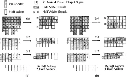
The comparison of the summation steps is illustrated in Fig. 4. In terms of the same transition numbers in summation steps, the proposed implementation uses 16 full adders and 2 half adders fewer than Yamazaki [7] proposed to use 16 full adders and 4 half adders.
C. Separated Signed Processing Architecture (SSPA)
The 2’s complement number representation for VLSI design will cause amounts of power consumption. For example, 0 in a 10 bit 2’s complement number rep- resentation is 0000000000 but -1 is 11 11 11 11 11. A lot of transitions will consume a large amount of power. To avoid the positive to negative transition, the Separated Signed Processing Architecture (SSPA) was proposed. Separated Signed Processing Architecture contains two parts, one is separated the negative
digits of coefficients from positive digits, and the other one is biasing the input data to positive.
Full Adder
0
I lalr AdderX: Arrival Time of Input Signal
a
Full Adder Result0 Half Adder Result
4:3 4:3
-
-
3:2 3:2
-
Lqqqqq
:$%/i%E:s
I=]
&!g$&S(a) (b)
Fig. 4. Comparison of summation steps. (a) The proposed method. (b) Yamazaki’s method.
Fig. 5 . Separated signed data path approach.
The coefficient ck is decomposed into positive (ckp) and negative ( c k n ) parts ac-
cording to the CSD representation. Two accumulating paths for each sign are finally utilized as in Fig. 5. For example, 0.010100101 is decomposed into 0.000100100 ( c k p ) and
-
0.010000001 ( c k n ) . As a result, this design processes thebiased input signal X in two different data paths for each sign without any con- trol. In order to avoid the transition between positive and negative caused by the input data, the filter input must be biased to a positive number instead of sign-magnitude representation. And delete these biases at the last stage of the accumulation path. In the case of 8-bit 2’s complement representation, bias
should be 128 and the biased input is between 0 and 255 instead of be- tween -128 and 127. The proposed bias can be easily achieved by inverting the most significant bit.
D. Modification to the CSD representation (MCSD)
Separated Signed Processing will produce the unbalance module. Because the occurrences of positive and negative digits have the same probability, it is just the average statistics. In practice, due to modularization, the distributions of positive and negative CSD digits are not uniform locally, the quantity of coeffi- cients need to be modified. The modification to the CSD representation is pro- posed to solve the above problem. The concept is to modify the CSD represen- tation to let the positive and negative parts balance, and the nonzero digits numbers are the same as before. For example, if the number of positive digits is much less than that of negative digits then 101 should be changed into 01 1 to increase the number of positive digits while decreasing the number of negative digits. On the contrary, when the situation is reversed, 101 could be changed into 011 to increase the number of negative digits.
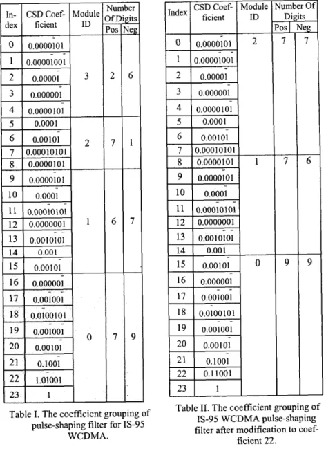
The quantized coefficients of the SRRC filter for the IS-95 WCDMA systems is
illustrated in Table I, where the depth of the carry-save adder tree is 4 and the maximal number of bits in the bit-plane is 9. In this example, module 2 has 7 positive digits but only 1 negative digit. Thus negative module 2 processes only one nonzero digit but still uses pipeline registers to separate itself from the negative module 3. slight modification to coefficient 22, the result will change dramatically. The original value of coefficient 22 is l.OT001 and modified to 0.11001, which keeps the same value and number of nonzero digits. The number of modules becomes 3 without affecting the timing as shown in Table 11. As a result, the number of pipelining registers is reduced. Evidently the modified CSD coefficients result in a structure that has high utilization of hardware, such as the registers and the adders.
__
CHIP IMPLEMENTATION
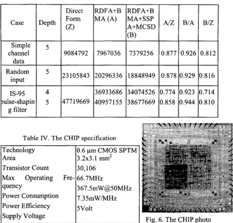
This section shows an example for IS-95 WCDMA pulse shaping FIR filter, which has 33-taps. The simulations used Verilog-XL tool with the ISM nonlinear model. Besides, compared with linear-phase direct form architecture for IS-95 WCDMA filters, obviously the modularization decreases the transition count as shown in Table 111. When the FIR filter is fed a sequence of randomly generating data, the result is also similar. For the IS-95 WCDMA pulse shaping filter, the proposed architecture can reduce the number of transitions to be 71.4%. This chip is fabricated in 0.6 pm SPTM CMOS technique. The Chip specification and CHIP photo are shown in Table IV and Fig. 6.
9 0.0000101
t+Z--l
- -18 11 0.00010101 12 0.0000001kl
0.0100101 1 17 18Table I. The coefficient grouping of pulse-shaping filter for IS-95
WCDMA. - -0.001001 0.0i00101 7 ~0.00010101
I
8 I0.0000101I
1I
19 0.001001I
0.0000101 11 0.00010101a
12 0.0000001I
20I
0.OOlOiI
I
13I
0 . 0 O l ~ o iI
Wl
23 16 0.000001 I I 19 20 21 22 23 0.001001 0.00101 0.1001 0.11001 19
-
6-
9Table 11. The coefficient grouping of IS-95 WCDMA pulse-shaping filter after modification to coef-
Table I11 Number of transitions of three cases. Case Simple channel data Random input IS-95 ulse-shapin g filter
Table IV. The CHIP specification
Technology 0.6 pm CMOS SPTM
Area 3.2x3.1 mm2
Transistor Count 30,106 Max Operating Fre- 66.7MHz
quency 367.5mW@50MHz
Power Consumption 7.35mW/MHz Power Efficiency 5Volt
Supply Voltage Fig. 6. The CHIP photo
CONCLUSIONS
In this paper, a low-power architecture for dedicated linear phase FIR filter is proposed. Four schemes are suggested, including re-timed structure, balanced modularized architecture, separated signed processing data flow and modifica- tion the CSD representation. From the experiment results, the proposed signal processing schemes contribute about ten to thirty percent of transition reduction in the accumulation path to achieve maximal efficiency of hardware compo- nents. Since FIR filter plays an important role for DSP and digital communica- tions, the proposed architecture will be very useful for the wireless embedded system design, especially for portable information applications.
REFERENCES
[l]. G. Wacey and D. R. Bull, “POFGEN: A Design Automation System for VLSI Digital Filters with Invariant Transfer Function,” IEEE International Symposium on Circuits and Systems, ISCAS, vol. 1, 1993, pp. 631 - 634. [2]. Mohammed Abo-Zahhad and Sabah Mohamed Ahmed, “Filter Designer: A
Complete Design and Synthesis Program for Lumped, Wave-Digital, FIR and IIR Filters,” Proceedings of the Thirteenth National Radio Science Conference, March 19-21, 1996, Cairo, Egypt, pp. C24.1 - C24.15. [3]. Varun Verma and Charles Chien, “A VHDL based Functional Compiler for
Optimum Architecture Generation of FIR Filters,” IEEE International Symposium on Circuits and Systems, ISCAS 1996, vol. 4, pp. 564 - 567.
[4]. Wolfgang Wilhelm and Tobias G. Noll, “A New Mapping Technique for Automated Design of Highly Efficient Multiplexed FIR Digital filters,” Proceedings of 1997 IEEE International Symposium on Circuits and Sys- tems, ISCAS 1997, vol. 4, pp. 2252 - 2255.
[5]. Rajeev Jain, Paul T. Yang, and Toshiaki Yoshino, “FIRGEN: A Com- puter-Aided Design System for High Performance FIR Filter Integrated Circuits,” IEEE Transactions on Signal Processing, vol. 39, no. 7, July [6]. Laskowski, J. and Samueli, H., “A 150-MHz 43-Tap Half-Band FIR Digital Filter in 1.2-um CMOS Generated by Silicon Compiler,” Proceedings of the Custom Integrated Circuits Conference, 1992, pp. 1 1.4.1-1 1.4.4.
[7]. Takao Yamazaki, Yoshihito Kondo, Sayuri Igota, Nonmembers, and Seiichiro Iwase, “”FASTOOL” an FIR Filter Compiler Based on the Automatic Design of the Multi-Input-Adder,” IEICE Trans. Fundaments, vol. E78-A, no. 12, December 1995, pp. 1699 - 1705